 Open Access
ARTICLE
Physical Properties of SiC Nanostructure for Optoelectronics Applications
1 Applied Science Department, University of Technology-Iraq, Baghdad, 10066, Iraq
2 Laser and Optoelectronic Engineering Department, University of Technology-Iraq, Baghdad, 10066, Iraq
* Corresponding Authors: Evan T. Salim. Email: ; Makram A. Fakhri. Email:
(This article belongs to the Special Issue: Current Advances in Green Nanomaterials Applications)
Journal of Renewable Materials 2021, 9(9), 1519-1530. https://doi.org/10.32604/jrm.2021.015465
Received 20 December 2020; Accepted 18 January 2021; Issue published 23 April 2021
Abstract
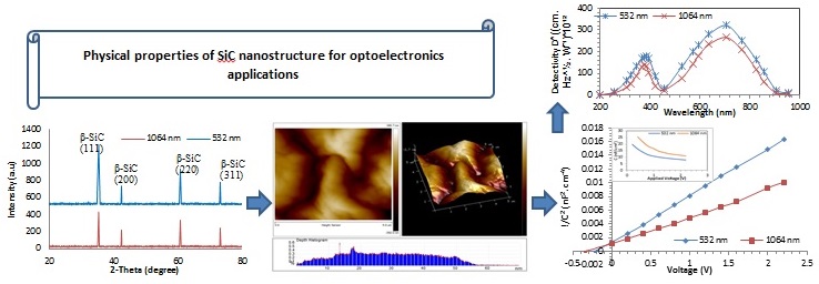
A SiC nanofilms have been deposited and investigated on quartz and silicon substrates using pulsed laser deposition technique with the 300 pulses of Nd: YAG laser at two different laser wavelengths of 1064 nm and 532 nm. The structural, morphological, and optical properties of the deposited nanostructure SiC were prepared and characterized as a function of the wavelengths of the used laser. The structural result shows four different pecks at (111), (200), (220), and (311) planes related to Nano SiC. The transmission result presents that the optical energy gap value for the SiC nanostructure is depended on the wavelength of the used laser and it is found about the range (3.03 eV–3.23 eV). The investigations of the SEM and AFM show that the prepared SiC Nano-films having a grain size range (36.34–48.75) nm and roughness about 4.462 to 3.062 nm. SiC/Si hetero-junction devices show an enhanced performance at 532 nm.Graphic Abstract

Keywords
Cite This Article
Citations
 Copyright © 2021 The Author(s). Published by Tech Science Press.
This work is licensed under a Creative Commons Attribution 4.0 International License , which permits unrestricted use, distribution, and reproduction in any medium, provided the original work is properly cited.


 Submit a Paper
 Propose a Special lssue
 View Full Text
 Download PDF

 Downloads
 Citation Tools