| Journal of Renewable Materials |
DOI: 10.32604/jrm.2021.014466
ARTICLE
Hydrogenated Amorphous Carbon Films from Palmyra Sugar
1Department of Physics, Faculty of Science and Data Analytics, Institut Teknologi Sepuluh Nopember, Kampus ITS Sukolilo, Surabaya, 60111, Indonesia
2Departement of Electronic Engineering, Faculty of Engineering, Universitas Muhammadiyah Malang, Malang, Indonesia
3Departement of Electronic Engineering, Faculty of Industrial Technology, Institut Teknologi Nasional Malang, Malang, Indonesia
4Synchrotron Light Research Institute, Nakhon Ratchasima, 3000, Thailand
*Corresponding Authors: Budhi Priyanto. Email: budhip67@gmail.com; Darminto. Email: darminto@physics.its.ac.id
Received: 29 September 2020; Accepted: 27 January 2021
Abstract: A simple, highly reproducible, and environmentally friendly method is a considered approach in generating renewable energy materials. Here, hydrogenated amorphous carbon (a-C) films have been successfully prepared from palmyra liquid sugar, employing spin-coating and spraying methods. Compared with the former method, the latter shows a significance in producing a better homogeneity in particle size and film thickness. The obtained films have a thickness of approximately 1000 to 100 nm and contain an sp2 hexagonal structure (~70%) and sp3 tetrahedral configuration (~30%) of carbons. The introduction of boron (B) and nitrogen (N) as dopants has created the local structural modification of bonding, inducing a slight change of electrical conductivity, electronic energy bandgap, and optical transparency near-infrared region. The obtained a-C film features a “green” semiconducting material.
Keywords: Thin film; palmyra sugar; amorphous carbon; boron; nitrogen
Carbon (C) is an element in the group IV periodic system that has similar characteristics as silicon (Si) and germanium (Ge) in the group. Unlike Si and Ge, C has a broad range of energy bandgap (Eg) between 0 and 6 eV, leading to a carbon compound as a good conductor, semiconductor, and even insulator [1]. There are three possible types of hybridized orbitals in carbon: sp, sp2, and sp3 configurations. In an amorphous state, carbon may configure in a mixed hybridized orbitals. Diamond is a crystalline carbon that is constituted by pure sp3 orbital to form a tetragonal structure, while graphite or graphitic compound contains pure sp2 orbital in constructing hexagonal bonding [2]. The mixture of hybridization between sp2 and sp3 develops an amorphous carbon structure (a-C). If the sp2 orbital is dominant, then the carbon compound is in a graphitic phase or glassy carbon [1,2]. An a-C with pure sp3 hybridization forms a diamond-like carbon (DLC), having inter-atomic bonds dominated by the sp3 orbital in a tetrahedral structure of carbon (ta-C) phase [3]. The DLC film’s properties have been dependent on the preparation method, hydrogen concentration, and deposition parameters. The hardness of carbon films depends on the sp3 hybridization content, while the non-hydrogenated carbon film and carbon nitride exhibit superior mechanical properties when the sp2 content is high [4]. The electronic properties of carbon are mainly dependent on the content of hybridized orbital. The carbon compound with pure sp3 hybridization characterizes an insulator. In contrast, the 100% sp2 hybridization in carbon material leads to a conductor. The hybridization of a mixture of sp2 and sp3 shows semiconducting properties depending on the sp2/sp3 ratio. Thus, a-C offers a wide range in tuning electrical properties and generating semiconducting features [2].
Carbon allotrophs, namely diamond, amorphous carbon, and their derivatives, have tremendous scale applications. Graphene, as the newest discovered carbon compound, consists of a sheet of hexagonal structured carbon atoms, having extraordinary electrical properties, unique optical properties, and high electrical mobility [1–4]. Graphene applications include transparent electrodes, solar cells, photodetector, transistor, supercapacitor, and other various applications [5]. These have provided the complimentary applications of carbon materials previously discovered, such as carbon nanotubes and fullerenes. With the various energy bandgap, the thin film of carbon can generally absorb sunlight that strikes it with good thermal and chemical stability [6]. Concerning the applications of photo-sensitive devices, solar cells utilized a-C doped with nitrogen (a-C:N) has successfully been fabricated using PECVD from camphor oil as a precursor. The cells with the configuration of Au/a-C:N/p-Si/Au have gained an efficiency of 0.000048% under 100 mW/cm2 illumination at 25°C. The a-C:N film has an Eg around 0.25–0.75 eV and an electrical conductivity of 0.016 Ω−1cm−1 [7]. As an anti-reflection material, the a-C, a-C:H, and ta-C have shown an excellent optical property compared to the conventional layers made of SnO2, ZnS, and MgF2 [8].
Recently, carbon compounds have begun to be synthesized from renewable resources, such as biomass or biowaste. Graphene derivatives compounds, in the form of reduced graphene oxide (rGO), have been successfully prepared from a biowaste of coconut shell [9–13]. Moreover, the glassy carbon has also been synthesized from the sap of palmyra (Borassus flabellifer) and coconut (Cocos nucifera) trees [14–16]. These carbon compounds have been examined to some extent, having comparable properties to the existing and commercial materials [9–18]. Thus, these are expected to provide renewable (green) carbon materials in the near future. Palmyra and coconut trees in Indonesia grow in the coastal lines of the main islands, such as Java, Madura, East Nusa Tenggara, and Sulawesi. The sap of palmyra and coconut, which are particularly the raw materials for brown sugar production, are also available throughout the year. It contains protein, fat, sucrose, glucose, minerals, calcium, and phosphorus, in which the sucrose is the main ingredient of palmyra and coconut sap, reaching ~75% of the total components. Glucose and sucrose are molecules that mainly contain carbon [15].
This paper reports the successful preparation of a-C in the forms of powder and films with palmyra sugar as the starting material, employing nano spraying and spin coating methods, which are relatively simple, environmentally friendly, and highly reproducible methods. The nanospray method, in particular, offers the reliability to produce films with the thickness in the order of a nanometer with a simple deposition process, does not cause pollutions during the process, and does not require a high power supply. Characterizations are performed as regards their structure and electronic properties. The effect of doping with boron (B) or nitrogen (N) atoms into the carbon network is also analyzed. The resulting films are characterized by analyzing phase and hybridization, morphology, electrical conductivity, and optical and electronic energy gap.
2.1 Preparation of Amorphous Carbon (a-C)
Brown sugar made of palmyra sap used as the starting material is illustrated in Fig. 1. The liquid sugar was heated using a hot plate at 150°C, stirred with a magnetic stirrer for 150 minutes to convert it into a slurry, and then cooled to room temperature to form a solid flake. The flake was then heated at 250°C in the air for 150 min inside a furnace to result in a very light and shiny black charcoal. The charcoal was then washed with distilled water employing the ultrasonic washing apparatus for 150 min and filtered three times to reduce the water content. The dried charcoal was thoroughly crushed to obtain a fine powder.
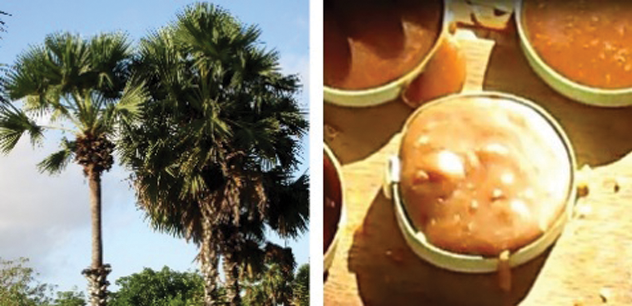
Figure 1: Palmyra tree and brown sugar made from palmyra sap
A mixture of 2 g carbon fine powder, 10 mL dimethyl sulfoxide (DMSO, Merck 99.9%) as a solvent, and 10 mL distilled water was prepared by a magnetic stirring hotplate with the speed of 1500 rpm for 60 min at 100°C. The mixture was then centrifuged (CENTRIFUGE 80-2) at 3500 rpm for 30 min to separate large particles from the carbon solution: Thus, the homogenous solution is achieved. We employed two simple methods in the film fabrication, namely spin-coating and spraying, using spin-coater (assembled by ITB) and nano-sprayer (30 ml USB Handy Nano Mist Sprayer), respectively. For the former method, the solution was dropped on a 2 × 2 cm2 ITO (indium tin oxide) coated–glass substrate. The substrate that has been dripped with carbon solution was rotated at 1400 rpm for 30 seconds and dried at room temperature, forming a carbon film on the substrate. For the latter method, the carbon solution was sprayed onto 1 × 2 cm2 of the ITO-glass substrate using nano-sprayer with the spraying time of 10 s. The distance between the ITO glass and sprayer hole was set to be a constant of 5 cm. Film drying was carried out at room temperature using a halogen lamp.
Boric acid (H3BO3, Merck 99.5%) and ammonium hydroxide (NH4OH, Merck 25%) were added to the carbon solution to prepare a-C films containing B (a-C:B) and N (a-C:N) atoms as dopants, respectively. The mol ratio of B or N to C is 1:15 (7% B or N). The film fabrication was conducted with the same methods as described above.
Structural characterizations aim to examine the phase formation, functional groups, and surface morphology, which were performed using X-ray diffraction (Philips X’Pert MPD) with Cu-Kα radiation in the diffraction angle range of 10 to 60°, Fourier transform infrared (FTIR, Shimadzu 8400S) spectrometer, and scanning electron microscope (SEM, ZEISS EVO 10), respectively. We utilized a synchrotron photoemission spectroscopy (syn-PES) at beamline 3.2a at Synchrotron Light Research Institute (SLRI), Thailand, to study the orbital hybridization and bonding among atoms O, H, B, and N with C as a host in the films. The measurement was performed in the x-ray photoemission (XPS) mode in an ultra-high vacuum condition (<1 × 10⁻⁵ Pa) with a photon energy range of 40–600 eV. By employing the Gaussian deconvolution functions with Shirley type background, fitting the experimental spectra was done using a software developed by SLRI as a part of the apparatus. The optical properties were measured using the UV-Vis spectrophotometer (GENESYS 10S) within the 400–1000 nm wavelength range. A four-point probe technique was employed to examine the electrical conductivity (σ) and electronic bandgaps (Eg) of films. Silver (Ag) paste was coated on the film to get good contact with the probe. The ohmic contact was confirmed before performing the measurements, indicated by a linear current-voltage (I-V) curve. The film’s conductivity (σ) is calculated from the response voltage and current by applying the formula: σ = I/(4πSV). Here, S, V, and I represent the distance between the probe, potential, and current, respectively [19].
3.1 Structural Properties of a-C Powder
Fig. 2a shows the XRD patterns of carbon powder from the heating process at 250°C, exhibiting a broad peak at around 20° with several sharp peaks. This shape characterizes that the sample is in an amorphous phase, constituted by irregularity in the crystal structure at the long-range order. The sharp peaks at 2θ of 28.4, 40.5, and 50.2° are identified as (002), (022), and (222) diffraction planes of the sylvite phase (KCl, JCPDS No. 00-041-1476). The KCl salt is generally present in palmyra product/sugar as an additional nutrient, which is absorbed from the soil during the growth of the tree’s xylem vessels and distributed to all parts, including panicles of flowers [16]. The panicle (inflorescence) is part of the palmyra tree that produces sap so that the sap, which is the starting material for palm sugar, indeed contains KCl. The SEM-EDX analysis of the a-C powder also suggests the presence of several elements, including C (53.66 wt%), O (41.36 wt%), Cl (1.73 wt%), Na (1.35 wt%), K (1.34 wt%), P (0.40 wt%), S (0.13%), and Si (0.03%). After rinsing with distilled water, the diffraction peaks of KCl disappeared from the sample to result in a clean amorphous carbon.
The functional groups of C=C, C-C, C-H, C-O, and O-H are identified from the FTIR spectrum, shown in Fig. 2b. These functional groups feature the bonding arrangement of sp2 and sp3 hybridized orbitals so that the ratio of sp2/sp3 orbitals in the sample can be estimated [20–22]. According to the FTIR spectrum, the sp2 content of 65–70% was obtained, indicating that the amorphous structure has been dominated by hexagonal (honeycomb) carbon structure with a minor tetrahedral configuration. Meanwhile, the sample morphology is given in the inset of Fig. 2a, visualizing that the powder contains coarse flake-like particles having a size in the scale of hundreds µm.
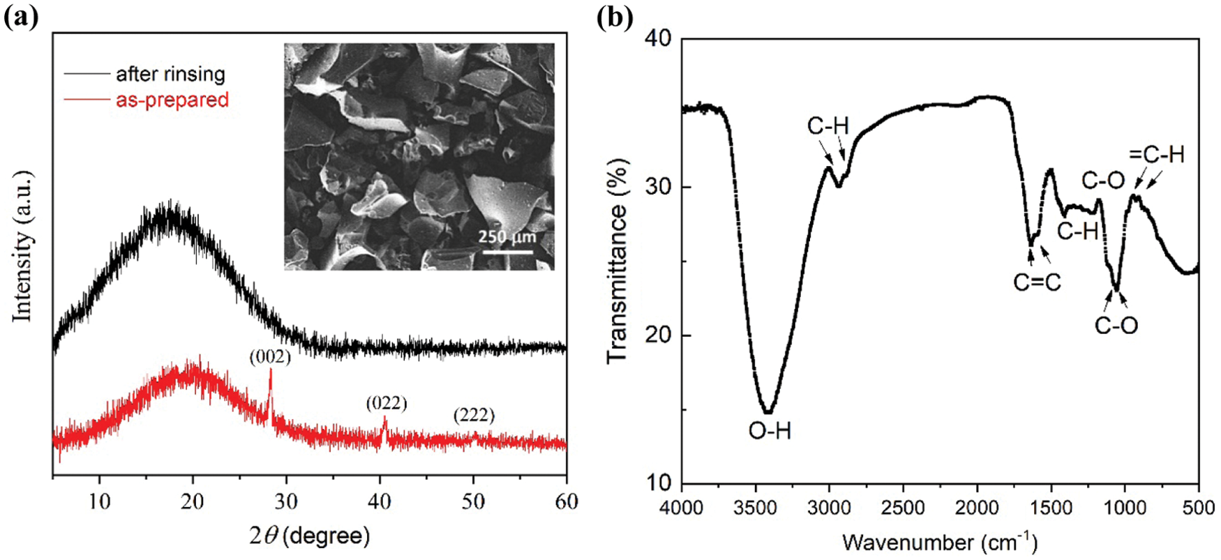
Figure 2: (a) X-ray diffraction patterns of as-prepared a-C powder and that after rinsing with distilled water. Miller indexes represent peaks of KCl salt. Inset is an SEM image of the rinsed a-C powder. (b) Fourier transform (FTIR) spectrum the a-C powder
3.2 Structural Characteristics of a-C Films
Presented in Fig. 3 are the XRD patterns of a-C films deposited by nano-spraying. The general look at the XRD profiles of those deposited by spin-coating (not presented here) is almost identical. The patterns are generally characterized by a single broad peak centered at around 23°. Compared to the powder sample above, this peak has slightly been shifted to a higher diffraction angle (~3°), being associated with the shortening distance between the adjacent hexagonal (graphene) layer in the a-C particles forming an amorphous film. Several sharp peaks have also been observed in all profiles, which belong to indium oxide (In2O3, JCPDS No. 00-006-0416) with plane (Miller) indexes of (211), (222), (400), and (440) [23] as a part of the substrate on the glass surface. The conductive characteristic of ITO offers a significance to facilitate direct contact with the a-C films, particularly in measuring photovoltaic effect in the fabricated pn-junction. One may also see that the introduction of N or B as dopants into the a-C films does not affect the diffraction pattern characteristics and the phase content. The dopants should, therefore, attach to the carbon network, which will be discussed later.
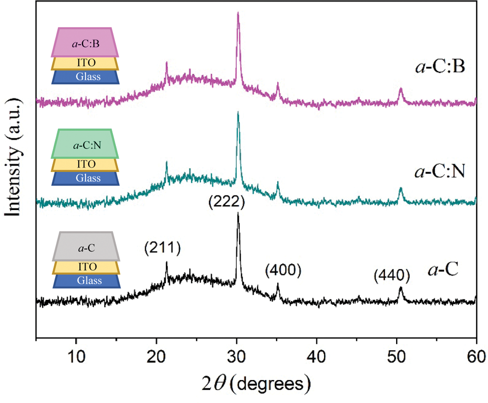
Figure 3: The XRD patterns of undoped (a-C), nitrogen (a-C:N), and boron (a-C:B) doped amorphous carbon films as specified. The indexes represent peaks of the ITO substrate. The film lining is illustrated in the insets
The deposition methods to fabricate film, spin-coating vs. nano-spraying, give significant differences in film thickness and morphology. As demonstrated in Figs. 4a and 4b, the thinnest film of about 2500 and 200 nm thickness was achieved by spin-coating and nanospray methods, respectively. The film deposited by the latter technique is more homogeneous than that by the former approach. Furthermore, having a look at the morphology, a-C particles are observed to have a size in micron-sized, from approximately 1 to 10 μm, and in hundreds of nm (submicron), as shown in Figs. 4c and 4d. It is clear from these two deposition techniques that the bigger sized particle has developed a thicker film. The two film deposition methods use the same carbon solution as the starting material, containing the exact size of carbon particles. The film deposited by the spin-coating grown from the carbon solution’s droplets flattened during the spinning process and then dried. This mechanism has led to particle aggregation, which may result in bigger particles size. Meanwhile, in the spraying method, the particle aggregation should be much reduced. As a result, the particles are expected to be kept individually in a smaller size, as seen in Fig. 4d. The nanospray method, up to this point, seems to have some advantages. Besides a better homogeneity in thickness and particle size, it also offers the ease of thickness adjustment through the deposition time. Spraying duration from 5, 10, 15, and 20 seconds has resulted in films having a 180–900 nm thickness. It means that the deposition rate is about 40–50 nm/s. SEM-EDX analysis shows the presence of In, Sn, Si, O, and C in the films, where a significant increase in the relative concentration of the C atom is observed after a-C’s deposition process onto the ITO substrate. This result is then confirmed by the XPS survey spectra, showing broad peaks of In 3d, Sn 3d, Si 2p, and S 2p.
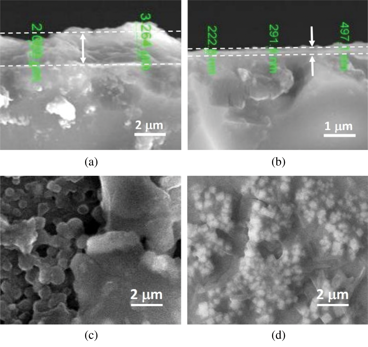
Figure 4: The SEM images of cross-sectional view and morphology of the a-C films deposited by spin-coating (a,c) and nanospray for 5 s (b,d)
3.3 Analysis of Hybridized Orbital Bonding of the Films
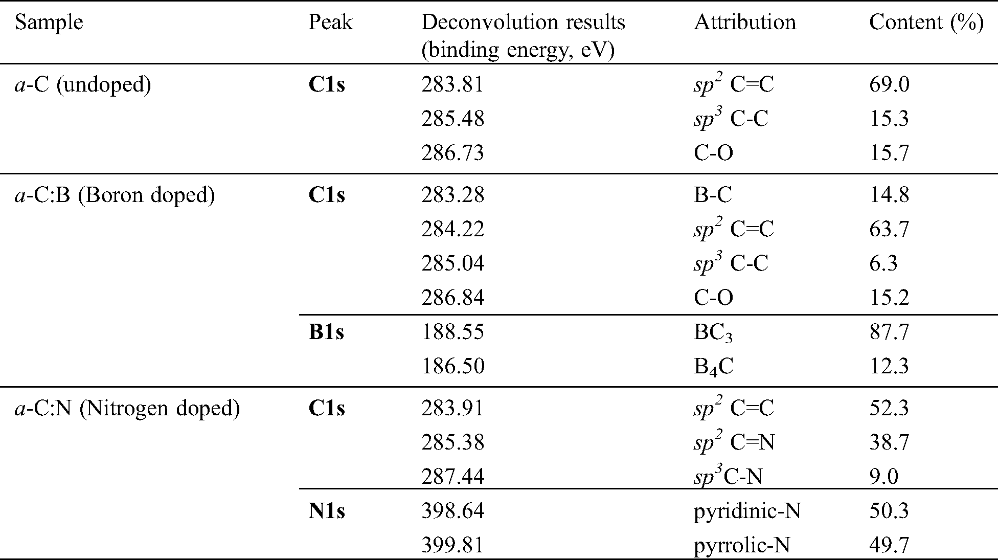
Going deeper to analyze the hybridized orbital bonding of a-C films concerning especially the structure upon N/B doping, we study the syn-PES spectra originating from electron transition from 1s atomic (orbital) level of carbon (C1s), nitrogen (N1s), and boron (B1s). Shown in Fig. 5 is the syn-PES spectrum of the undoped a-C sample. Analysis of the C1s peak of the a-C film indicates the presence of sp2 C=C, sp3 C-C, and C-O orbitals, each at the corresponding binding energy of 283.8, 285.4, and 286.7 eV. The content of each bonding type was calculated from the ratio of each convoluted peak’s area to the total area. The sp2 C=C component, for example, is estimated by dividing the C=C peak area by the total C1s peak area. Hence, the percentage of sp2 C=C, sp3 C-C, and C-O orbitals in the a-C film is approximately 69.0, 15.4, and 15.7%, respectively, as summarized in Tab. 1. This result confirms the estimation obtained from FTIR data discussed above, that the sp2 content in the a-C powder is around 65 to 70%. According to the ternary phase diagram of the carbon-hydrogen system [1], this a-C sample is close to the glassy carbon phase. Our other films fabricated using a plasma-enhanced chemical vapor deposition (PE-CVD) from methane (CH4) gas contains more than 70% of sp3, revealing the tetrahedral carbon (ta-C) phase, which closes to the DLC characteristic [24].
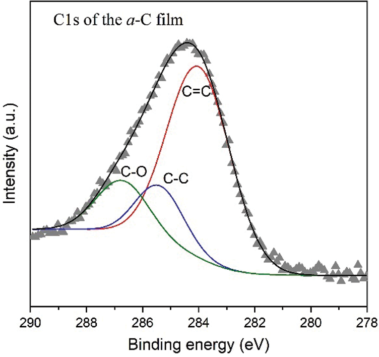
Figure 5: The C1s synchrotron PES spectrum of the undoped a-C film with convoluted peaks attributed to C=C, C-C, and C-O
The C1s spectrum of the a-C:B film (not shown here) contains four peaks describing sp2 C=C, sp3 C-C, C-O, and B-C bonds with corresponding binding energy summarized in Tab. 1. The presence of B-C bonding proves that the boron successfully attaches to carbon and converts the sp3 bond to the sp2 one, without any disturbance on the C-O bond. The same effect has also been reported previously [25], stating that boron doping can reduce sp3 hybridization. Furthermore, the deconvolution of the B1s spectrum has given two peaks centered at 188.5 and 186.5 eV, each of which is the BC3 (87.7%) and B4C (12.3%) configurations showing the formation of B-C bonds. In the BC3 configuration, a carbon is replaced by boron in the framework, whereas in the B4C bonding structure, a carbon vacancy is created [26]. The BC3 presence should enable an increased electrical conductivity since there is a lack of one electron due to the C=C bond replaced by B-C, and the valence band structure and state density near the Fermi level of carbon can be changed by this boron doping [27].
Three peaks are deconvoluted from the syn-PES C1s spectrum of the a-C:N film, indicating the presence of the sp2 C=C, sp2 C=N, and sp3 C-N bondings. It means that nitrogen in the a-C network is surrounded only by two neighboring carbons with π bond (38.7%), which is much more dominant than by three carbons with σ bond (9.1%). The substitution of a double bond carbon by N requires less energy than a single bond; thus, a small amount of nitrogen can easily replace carbon atoms in a network of double bonds. As a result, the sp2 bond in the layer increases, which is in line with previously reported studies [28,29]. The amorphous carbon layer with the increased sp2 hybridization in the presence of nitrogen produces a higher conductivity [19].
Furthermore, the deconvolution result of the N1s spectrum shows that there are two components, which are centered at 398.6 and 399.8 eV, namely as the pyridinic-N and pyrrolic-N phases. These two configuration types are constructed in the conjugated system (π bonding) and attached to two adjacent carbons. The pyridinic-N state contributes one electron to the π system, while the pyrrolic-N phase contributes two electrons [29]. Among these types of nitrogen bonds, pyridinic-N is sp2 hybridization, and the pyrrolic N is sp3 one. The a-C:N sample has a slightly higher concentration of pyridinic-N compared to pyrrolic-N. A hexagonal ring has three double bonds in the pyridinic bonds, where six electrons are delocalized and form π bonds. The nitrogen atom uses one electron to form the π bond, two electrons to form the σ bond, and the other two electrons are still in a pair of non-binding state. Whereas in the pyrrolic state, the pentagonal ring has two double bonds. The nitrogen consequently uses its two electrons in non-bonding orbital to contribute to the π system, which is delocalized. There should be no free electron in this configuration [29].
Table 1: The analyses results on syn-PES data of the a-C films. Attribution of the deconvoluted peaks refers to references [26–29]
3.4 Electrical and Optical Properties of the Films
Tab. 2 lists the estimated conductivity and bandgap from the measurements. The electrical conductivity of the films is approximately 0.5 Ω−1cm−1. It is important to note that the electrical conductivity of all a-C films is in the range of semiconducting materials, from hundreds to thousands as higher as that of amorphous silicon (a-Si) film. The electrical conductivity of a-Si films at room temperature is in the order of 10−5 to 10−4 Ω−1cm−1 [30,31]. To evaluate the electronic bandgap, we also employ the conductivity measurement upon elevating temperature from room temperature to around 90°C. Using the formula: σ = σ0 exp(-Eg)/2kT, we can estimate Eg from the slope of the ln(σ/σ0) vs. 1/T plot. Here, Eg and T are the energy (electronic) bandgap and temperature, respectively, σ0 is the initial conductivity, and k is the Boltzmann’s constant (8.617 × 10⁻⁵ eV K−1) [19]. Fig. 6 presents the plot of ln(σ/σ0) vs. 1/T of the a-C film prepared by the nano-spraying method. A linear fitting to the data results in the gradient of about −659.91, which gives the value of Eg = −2k(−659.91) ≈ 0.113 eV. The same procedure is applied to estimate the Eg of a-C:B and a-C:N films, which yields the values of approximately 0.090 and 0.060 eV, respectively.
Table 2: The electrical conductivity and electronic bandgap of the a-C films
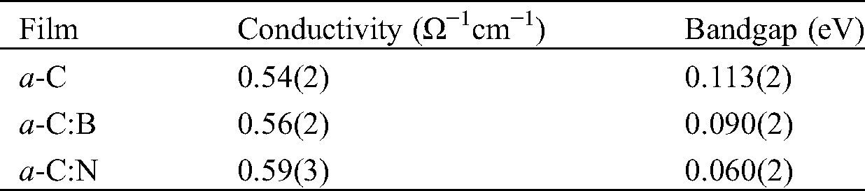
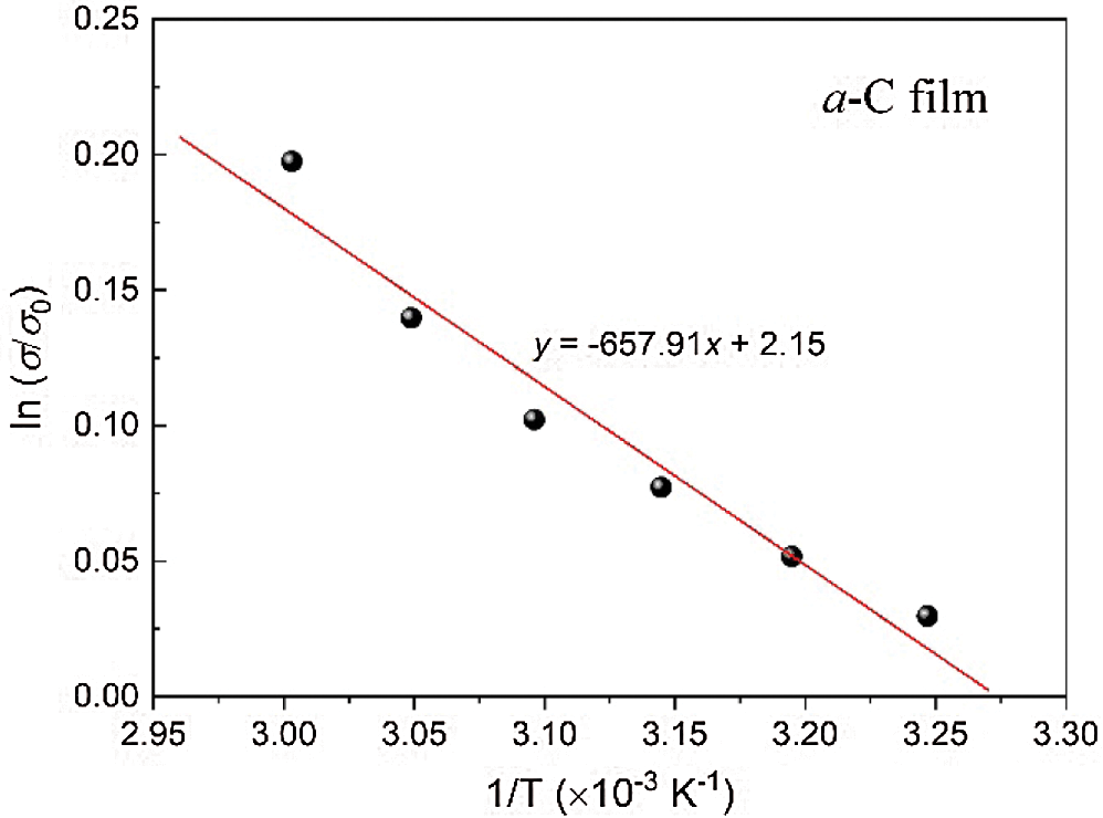
Figure 6: The plot of ln(σ/σ0) vs. 1/T of the a-C film prepared by the nano-spraying method. The solid line is the linear fitting to the data
Furthermore, their bandgap is in the range of that belonging to the glassy phase of carbon (Eg ≈ 0.01 eV) and evaporated carbon (Eg ≈ 0.4 eV) [1]. Our a-C film fabricated using a PECVD method [24] with ~30% of sp2 hybridized bonds has Eg = 2.0–2.5 eV, which is in the range of a tetrahedral carbon (ta-C:H). It should be noted that the electrical conductivity and electronic bandgap of the a-C films are slightly varied upon doping. Despite the content of sp2 hybridization in a-C:N increases and the BC3 bond is realized in a-C:B, the electrical conductivity does not significantly enhance. We expect that some electrons might be trapped by functional groups present in the films; thus, they are cannot freely mobile [27,32,33]. Over B-doped could also give rise to lowering conductivity [27].
The UV-Vis spectra of the a-C films are illustrated in Fig. 7. The optical transmittance is generally presented by the same curves for all films, although the absolute value is slightly reduced upon doping. The maximum transparency of all films is centered around the wavelength of 900 nm, which is equivalent to a radiant energy ~1.37 eV. The absolute value of transparency belongs to the undoped a-C film (~ 95%) and decreases (down to ~70%) due to doping.
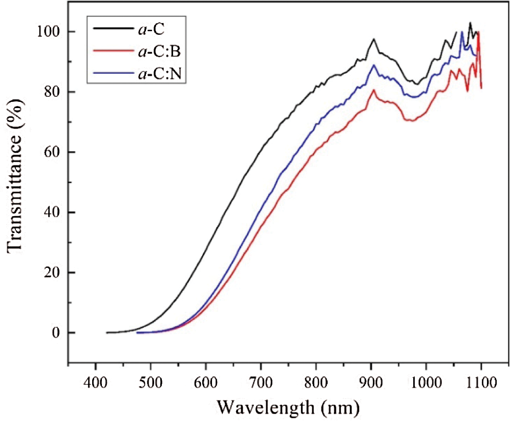
Figure 7: The UV-Vis spectra of the a-C, a-C:B, and a-C:N films
The amorphous carbon materials have successfully been prepared from palmyra liquid sugar to produce powder and thin films on the ITO substrate. The film fabrication employs two methods, namely the spin coating and nano-spraying. The latter method shows a significance in producing a better homogeneity in particle size and a thinner film than the former as it reduces particle aggregation. The spraying method enables to deposit films with a thickness of around 100 nm. B and C dopants have also been successfully introduced into the a-C film with the significant hexagonal carbon structure, inducing free electrons created from the C–B and C–N bondings and their defects. As a result, the deposited film has characterized a semiconducting behavior which is transparent in the near-infrared region of the electromagnetic radiation. These a-C films and the powder prepared from the palmyra sugar as a biomass product can be considered “green” materials.
Funding Statement: One of us (BP) would like to thank the Ministry of Finance and the Ministry of Research, Technology, and Higher Education for providing the LPDP BUDI-DN scholarship. The use of the synchrotron PES facility at SLRI (Public Organization), Thailand, would also be appreciated. This work is partially supported by Institut Teknologi Sepuluh Nopember, under contract No. 863/PKS/ITS/2020.
Conflicts of Interest: The authors declare that they have no conflicts of interest to report regarding the present study.
1. Robertson, J. (2002). Diamond like amorphous carbon. Materials Science and Engineering, R, 37(4–6), 129–281. DOI 10.1016/S0927-796X(02)00005-0. [Google Scholar] [CrossRef]
2. Furlan, K. P., Klein, A. N., Hotza, D. (2013). Diamond like carbon deposited by hydrocarbon plasma sources. Reviews on Advanced Materials Science, 34, 165–172. [Google Scholar]
3. Kenzie, M. (1996). Tetrahedral bonding in amorphous carbon. Reports on Progress in Physics, 59(12), 1611–1664. DOI 10.1088/0034-4885/59/12/002. [Google Scholar] [CrossRef]
4. Wang, C., Yang, S., Wang, Q., Wang, Z., Zhang, Y. (2008). Comparative study of hydrogenated diamond like carbon film and hard hydrogenated graphite like carbon film. Journal of Applied Physics, 103(12), 123531. DOI 10.1063/1.2938747. [Google Scholar] [CrossRef]
5. Darminto, Baqiya, M. A., Asih, R. (2018). Pengembangan bahan karbon dari biomassa. Indonesia: ITS Press. [Google Scholar]
6. Risplendi, F., Bernardi, M., Cicero, G., Grossman, J. C. (2014). Structure property relations in amorphous carbon for photovoltaics. Applied Physics Letter, 105(4), 043903. DOI 10.1063/1.4891498. [Google Scholar] [CrossRef]
7. Fadzilah, A. N., Dayana, K., Rusop, M. (2012). Carbon based solar cell from amorphous carbon with nitrogen incorporation. Journal of Advanced Material Research, 576, 785–788. DOI 10.4028/www.scientific.net/AMR.576.785. [Google Scholar] [CrossRef]
8. da Silva, D. S., Côrtes, A. D. S., Olivera, M. H.Jr, Motta, E. F., Viana, G. A. (2011). Application of amorphous carbon based materials as antireflective coatings on crystalline silicon solar cells. Journal of Applied Physics, 110(4), 043510. DOI 10.1063/1.3622515. [Google Scholar] [CrossRef]
9. Darminto, D., Koike, Y., Asih, R., Kurniasari, K., Baqiya, M. A. et al. (2018). Enhanced magnetism by temperature induced defects in reduced graphene oxide prepared from coconut shells. IEEE Transactions on Magnetics, 54(10), 1600105. DOI 10.1109/TMAG.2018.2864946. [Google Scholar] [CrossRef]
10. Jayanti, D. N., Nugraheni, A. Y., Kurniasari, K., Baqiya, M., Darminto. (2017). Photoluminescence of reduced graphene oxide preprared from old coconut shell with carbonization process at varying temperature. IOP Conference Series: Materials Science and Engineering, 196, 012005. DOI 10.1088/1757-899X/196/1/012005. [Google Scholar] [CrossRef]
11. Mas’udah, K. W., Nugraha, I. M. A., Abidin, S., Mufid, A., Astuti, F. et al. (2016). Solution of reduced graphene oxide synthesized from coconut shell and its optical properties. AIP Conference Proceeding, 1725, 020045. [Google Scholar]
12. Baqiya, M. A., Nugraheni, A. Y., Islamiyah, W., Kurniawan, A. F., Ramli, M. M. et al. (2020). Structural study on graphene-based particles prepared from old coconut shell by acid–assisted mechanical exfoliation. Advanced Powder Technology, 31(5), 2072–2078. DOI 10.1016/j.apt.2020.02.039. [Google Scholar] [CrossRef]
13. Ristiani, D., Asih, R., Puspitasari, N. S., Baqiya, M., Risdiana et al. (2020). Introduction of Na+ in reduced graphene oxide prepared from coconut shells and its magnetic properties. IEEE Transactions on Magnetics, 56(7), 2700106. DOI 10.1109/TMAG.2020.2994175. [Google Scholar] [CrossRef]
14. Pamungkas, D. I., Haikal, A., Baqiya, M. A., Cahyono, Y. Darminto et al. (2018). Synthesis of amorphous carbon from bio-products by dry method. AIP Conference Proceedings, 1945, 020059. [Google Scholar]
15. Pamungkas, D. I., Mu, M., Priyanto, B., Nakajima, H., Tunmee, S. et al. (2019). Structural analysis and electrical properties of amorphous carbon thin film. Materials Science Forum, 966, 66–71. DOI 10.4028/www.scientific.net/MSF.966.66. [Google Scholar] [CrossRef]
16. Mukarromah, Pamungkas, D. I., Darminto, D. (2019). Structural characterization of amorphous carbon film from palmyra sap. AIP Conference Proceeding, 2120, 050012. [Google Scholar]
17. Asih, R., Yutomo, E. B., Ristiani, D., Baqiya, M. A., Kawamata, T. et al. (2019). Comparative study on magnetism of reduced graphene oxide (rGO) prepared from coconut shells and the commercial product. Material Science Forum, 966, 290–295. DOI 10.4028/www.scientific.net/MSF.966.290. [Google Scholar] [CrossRef]
18. Asih, R., Septya, M. M., Yutomo, E. B., Astuti, F., Baqiya, M. A. et al. (2020). Physical properties comparison of rGO-like phase prepared from coconut shell and the commercial product. Jurnal Fisika dan Aplikasinya, 16(2), 82–86. DOI 10.12962/j24604682.v16i2.6712. [Google Scholar] [CrossRef]
19. Ray, S. C., Mbiombi, W., Papakonstantinou, P. (2014). Electrical and electronic properties of nitrogen doped amorphous carbon (a-CNx) thin films. Current Applied Physics, 14(12), 1845–1848. DOI 10.1016/j.cap.2014.10.016. [Google Scholar] [CrossRef]
20. Tucureanu, V., Matei, A., Avram, A. M. (2016). FTIR spectroscopy for carbon family study. Critical Reviews in Analytical Chemistry, 46(6), 502–520. DOI 10.1080/10408347.2016.1157013. [Google Scholar] [CrossRef]
21. Veres, M., Koós, M., Pócsik, I. (2002). IR study of the formation process of polymeric hydrogenated amorphous carbon film. Diamond and Related Materials, 11(3–6), 1110–1114. DOI 10.1016/S0925-9635(02)00011-0. [Google Scholar] [CrossRef]
22. Awang, R. (2008). PECVD hydrogenated amorphous carbon films: Growth and characterization(Ph.D. Thesis). University of Malaya, Malaysia. [Google Scholar]
23. Parsianpour, E., Raoufi, D., Roostaei, M., Sohrabi, B., Samavat, F. (2017). Characterization and structural property of indium tin oxide thin films. Advances in Materials Physics and Chemistry, 7(02), 42–57. DOI 10.4236/ampc.2017.72005. [Google Scholar] [CrossRef]
24. Priyanto, B., Saleh, M., Tunmee, S., Euaruksakul, C., Cahyono, Y. et al. (2019). Fabrication of amorphous carbon thin film from CH4 using PEVCD. Materials Science Forum, 966, 95–99. DOI 10.4028/www.scientific.net/MSF.966.95. [Google Scholar] [CrossRef]
25. Tan, M., Zhu, J., Han, J., Gao, W., Niu, L. et al. (2007). Chemical analysis and vibrational properties of boronated tetrahedral amorphous carbon films. Diamond and Related Materials, 16(9), 1739–1745. DOI 10.1016/j.diamond.2007.06.004. [Google Scholar] [CrossRef]
26. Yu, X., Han, P., Wei, Z., Huang, L., Gu, Z. et al. (2018). Boron-doped graphene for electrocatalytic N2 reduction. Joule, 2(8), 1610–1622. DOI 10.1016/j.joule.2018.06.007. [Google Scholar] [CrossRef]
27. Chiang, W. H., Chen, G. L., Hsieh, C. Y., Lo, S. C. (2015). Controllable boron doping of carbon nanotubes with tunable dopant functionalities: An effective strategy toward carbon materials with enhanced electrical properties. RSC Advances, 5(118), 97579–97588. DOI 10.1039/C5RA20664B. [Google Scholar] [CrossRef]
28. Hayashi, Y., Yu, G., Rahman, M. M., Krishna, K. M., Soga, T. (2001). Spectroscopic properties of nitrogen doped hydrogenated amorphous carbon films grown by radio frequency plasma-enhanced chemical vapor deposition. Journal of Applied Physics, 89(12), 7924–7931. DOI 10.1063/1.1371268. [Google Scholar] [CrossRef]
29. Wei, D., Liu, Y., Wong, Y., Zhang, H., Huang, L. et al. (2009). Synthesis of N-doped graphene by chemical vapor deposition and its electrical properties. Nano Letters, 9(5), 1752–1758. DOI 10.1021/nl803279t. [Google Scholar] [CrossRef]
30. Le Comber, P. G., Mort, J. (1973). Electronic and structural properties of amorphous semiconductors. New York: Academic Press. [Google Scholar]
31. Prayogi, S., Baqiya, M. A., Cahyono, Y., Darminto. (2019). Optical transmission of p-type a-Si:H thin film deposited by PECVD on ITO-coated glass. Materials Science Forum, 966, 72–76. DOI 10.4028/www.scientific.net/MSF.966.72. [Google Scholar] [CrossRef]
32. Shen, W., Li, H., Wang, C., Li, Z., Xu, Q. (2015). Improved electrochemical performance of the Na3V2(PO4)3 cathode by B-doping of the carbon coating layer for sodium-ion batteries. Journal of Materials Chemistry A, 3(29), 15190–15201. DOI 10.1039/C5TA03519H. [Google Scholar] [CrossRef]
33. Wang, C., Guo, Z., Shen, W., Xu, Q., Liu, H. et al. (2014). B-doped carbon coating improved the electrochemical performance of electrode materials for Li-ion batteries. Advanced Functional Materials, 24(35), 5511–5521. DOI 10.1002/adfm.201401006. [Google Scholar] [CrossRef]
 | This work is licensed under a Creative Commons Attribution 4.0 International License, which permits unrestricted use, distribution, and reproduction in any medium, provided the original work is properly cited. |