
 Submit a Paper
 Propose a Special lssue
 Open Access
ARTICLE

Effect of Different Etching Time on Fabrication of an Optoelectronic Device Based on GaN/Psi
1 Laser and Optoelectronic Engineering Department, University of Technology-Iraq, Baghdad, Iraq
2 Department of Civil Engineering, College of Engineering, Cihan University-Erbil, Kurdistan Region, Iraq
3 Department of Petroleum and Gas Refinery Engineering, Al-Farabi University Collage, Baghdad, Iraq
4 Applied Science Department, University of Technology-Iraq, Baghdad, Iraq
5 Department of Medical Physics, Al-Mustaqbal University College, Babylon, Iraq
6 Institute of Nano Electronic Engineering, University Malaysia Perlis, Kangar, Perlis, Malaysia
* Corresponding Authors: Haneen D. Jabbar. Email: ; Makram A. Fakhri. Email:
,
(This article belongs to the Special Issue: Carbon-Based Nanomaterials from Renewable Materials: Synthesis, Properties and Applications)
Journal of Renewable Materials 2023, 11(3), 1101-1122. https://doi.org/10.32604/jrm.2023.023698
Received 10 May 2022; Accepted 22 July 2022; Issue published 31 October 2022
 View Full Text
 Download PDF
Abstract
Gallium nitride (GaN)/porous silicon (PSi) film was prepared using a pulsed laser deposition method and 1064 nm Nd: YAG laser for optoelectronic applications and a series of Psi substrates were fabricated using a photoelectrochemical etching method assisted by laser at different etching times for 2.5–15 min at 2.5 min intervals. X-ray diffraction, room-temperature photoluminescence, atomic force microscopy and field emission scanning electron microscopy images, and electrical characteristics in the prepared GaN on the Psi film were investigated. The optimum Psi substrate was obtained under the following conditions: 10 min, 10 mA/cm2, and 24% hydrofluoric acid. The substrate exhibited two highly cubic crystalline structures at (200) and (400) orientations and yellow visible band photoluminescence, and homogeneous pores formed over the entire surface. The pores had steep oval shapes and were accompanied by small dark pores that appeared topographically and morphologically. The GaN/Psi film fabricated through PLD exhibited a high and hexagonal crystallographic texture in the (002) plane. Spectroscopic properties results revealed that the photoluminescence emission of the deposited nano-GaN films was in the ultraviolet band (374 nm) related to GaN material and in the near-infrared band (730 nm) related to the Psi substrate. The topographical and morphological results of the GaN films confirmed that the deposited film contained spherical grains with an average diameter of 51.8 nm and surface roughness of 4.8 nm. The GaN/Psi surface showed a cauliflower-like morphology, and the built-in voltage decreased from 3.4 to 2.7 eV after deposition. The fabricated GaN/Psi film exhibited good electrical characteristics.Keywords
III-nitride semiconductor materials, such as AlN, InN, and GaN, are widely used in the fabrication of modern optoelectronic devices because of their unique features for scientific and technological applications [1–3]. Gallium nitride (GaN) is one of the III-nitride semiconductor materials with different forms (powder, films, and nanoparticles) [4,5]. GaN has high electron mobility, high carrier saturation velocity, high thermal conductivity, a wide band gap of 3.4 eV, and a high optical absorption coefficient [6–9]. GaN-based optoelectronic devices include light-emitting diodes (LEDs), photodiodes, ultraviolet detectors, and high-power and high-frequency optoelectronic devices [10,11]. GaN devices can operate in fast and harsh environments and are thus ideal for photodiodes with small dimensions, good thermal and chemical stability, and low dark current and high breakdown field [12–14]. The gaN-based photodiode has interesting applications in civil and military, such as chemical sensing and heat, flame, and missile detection [15,16]. These features render optoelectronic devices operational in blue to near-ultraviolet spectral regions. Furthermore, GaN has a high temperature, power, and high frequency [17,18].
Several GaN thin-film deposition processes have been used, including chemical vapor deposition (CVD), such as molecular beam epitaxial, atmospheric pressure CVD, low-pressure CVD, plasma-enhanced CVD, metal-organic CVD, and hot wire CVD, and physical vapor deposition process, such as pulsed laser deposition (PLD) [19–23]. The PLD of III-nitride semiconductor materials has many distinct benefits, including simple method, versatility, rapid production of films with a strong forward-directed plume of materials that can be deposited with low pollution and specific stoichiometry [24–27]. Moreover, coating stoichiometry, crystallinity, topography, morphology, and roughness can be regulated by adjusting deposition parameters [28,29].
Porous silicon (Psi) is one of the most promising materials because of its excellent properties, showing great potential as a substrate for optoelectronic devices, such as sensors, LEDs, photodiodes, detectors, and computer chips [30–32]. One of the most important characteristics of the Psi layer is its large and reactive interior surface, which is considered the most critical property of Psi [33–36]. A Psi layer is different from bulk silicon because of its unique characteristics, such as strong visible photoluminescence (PL) at room temperature, direct bandgap, low cost, quantum confinement effect that promotes radiative transition, a high point of chemical reactivity and quick oxidation, which make Psi as a potential substrate for integrated optics and photonics devices [37,38].
The goal of this research is to study the effect of using different etching times in the preparation of Psi with the photoelectrochemical etching method. A solid-state laser (Nd: YAG laser) with a wavelength of 1064 nm was used in preparing a Gallium nitride on porous silicon (GaN on a Psi) “GaN/Psi” substrate with PLD. The deposition was carried out using laser energy of 1000 mJ and a vacuum pressure of 10−2 Torr. The effects of varying etching times on structural, spectroscopic, morphological, topographical, and electrical characteristics of GaN structure on a Psi substrate were explored in the present study.
2.1 Preparation of Psi Substrate
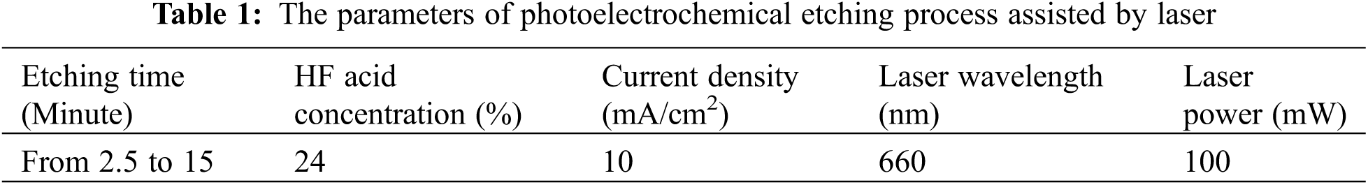
Silicon wafers (N-Type) (crystalline silicon, University Wafer, Inc., USA) of 500 μm thickness, 0.001–0.005 Ω/cm electrical resistivity “According to Saxena et al. [39], resistivity affects the porous silicon’s morphological structure. Where higher resistivity Si wafers produce aligned Si nanowire arrays-like structure after etching, whereas relatively lower resistivity Si wafers produce an interconnected porous (cheese-like) structure. But all the porous resistivity has visible photoluminescence due to the quantum confinement effect and that is all we need in our work” and (100) orientations were used in fabricating Psi substrate at room temperature with a photo-electrochemical etching method assisted by a diode laser of 660 nm wavelength and 100 mW power (China, Tongtool Company), DC power supply (0–30 V; China, Jiuyuan), digital multimeter (China, Victor Company, VC97), magnification beam expander of 10× (China, Carman Haas Company), electrolyte solution of 48% hydrofluoric acid (German, Thomas Baker Company) and 99.9% ethanol (German, Honeywell company). Si wafers were cut into 1 × 1 cm squares and cleaned with ultrasonic equipment in 99.9% ethanol for 5 min for the removal of surface contaminants and oxidation. The top-down approach of photoelectrochemical etching setup assisted by laser was used in preparing the Psi substrate. Additionally, the process was carried out using a Teflon cell with platinum electrodes with a purity of 95% (turkey) as cathode and silicon as the anode, as shown in Fig. 1.

Figure 1: Schematic diagram of photoelectrochemical etching process assisted by laser to prepare Psi substrates
Table 1 shows the parameters of the top-down photoelectrochemical etching process assisted by a laser for the preparation of Psi. The electrolyte concentration of HF: ethanol was fixed to 24% concentration with dilution equation [40–42], as shown in Eq. (1).
where:
A highly impure GaN powder of 99.9% (Luoyang Advanced Material Company, China) was used in the pulsed laser deposition method and prepared by pressing GaN powder with a hydraulic press of 15 Kg cm2. The obtained GaN sample was circular, 5 gm, 2 cm in diameter, and 0.5 cm in thickness.
2.3 Preparation of GaN Films by PLD
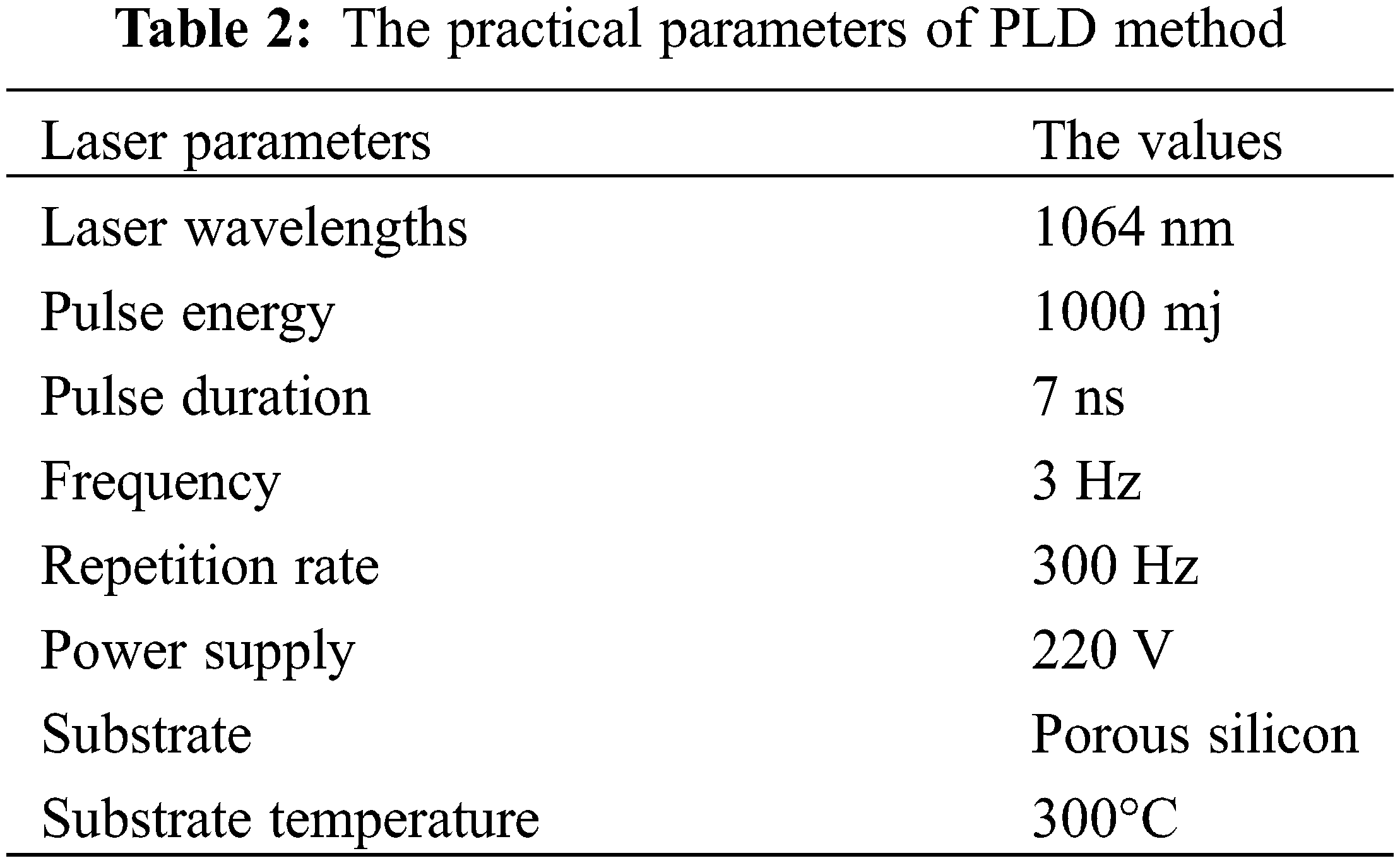
A Q-Switching Nd: YAG laser (Guangzhou Dany Optical Technology Co., Ltd., China) with the energy of 1000 mJ, wavelengths of 1064 nm, and pulse duration of 7 ns was used in ablating the GaN target to deposit on the prepared Psi substrate. The process of PLD was carried out with a vacuum pressure of 10−2 mbar with practical parameters as presented in Fig. 2, and indicated in Table 2.

Figure 2: Schematic diagram of PLD method of GaN on Psi substrate using different wavelengths 1064, 532, and 355 nm
2.4 Preparing of Fingerprint Mask on GaN Films
A fingerprint mask-like aluminum (AL) mask has been deposited on the fabricated GaN films by a thermal evaporation system under 5 × 10⁻⁵ mbar for the maintenance of nanostructure performance. Fig. 3 shows the preparation processes of GaN-film-based optoelectronic devices.

Figure 3: Schematic illustration of the fabricated GaN/Psi optoelectronic device
2.5 Characterization by XRD, PL, FESEM, and AFM
Psi substrate and GaN thin film undergo several tests, such as X-ray diffraction (XRD) from Japan (XRD6000 Shimadzu Company) with copper radiation of 1.54060 Å was used in testing structural characteristics. Field emission scanning electron microscopy (FESEM) from German (ZEISS Company) was used in testing morphological properties with high resolution. Furthermore, atomic force microscopy (AFM) from the United States of America (TT-2 Workshop Company) was used in testing topographical properties. PL from the United States of America (Perkin Elmer Company) was used in testing spectroscopic properties.
2.6 Electrical Characterization
The current-voltage characteristics of Psi substrates and GaN thin film in dark and light for forward and reverse bias was investigated using a power supply (China, DAZHENG, 30 Volt, 5 A, PS-305D) and digital multimeters (UNI-T-UT33C) and (TEKR, CDM 250). Capacitance–voltage characteristic was explored using a programmable LCR meter (Taiwan, GW INSTEK, LCR-6100, and 10 Hz–100 kHz).
Fig. 4a shows the XRD patterns of the N-type Si <100> oriented wafer before the etching process, the Si <100> crystalline phase is the sole peak seen in the XRD pattern, indicating that no other crystalline phases were presented [43–45]. Fig. 4b shows the XRD patterns of the porous Si prepared at different etching times and the main substrates (N-Type Si). The main peaks were observed at etching times of 2.5, 5, 12.5, and 15 min, which mainly corresponded to (111) and (400) planes. Two main peaks were observed at etching times of 7.5 and 10 min, which mainly corresponded to the (200) and (400) planes. These peaks were indexed and consistent with the diffraction data of a silicon standard (JCPDS card 27-1402). A high and optimum crystallinity texture of the porous silicon structure appeared at an etching time of 10 min, according to Sampath et al. [46–48], and Fig. 4c presents the main peak (400), and it is clear that its splatted to two peaks one for Si and other for Psi [43].

Figure 4: XRD pattern (a) N-type Si, (b) prepared Psi substrates by photoelectrochemical etching method assisted by laser at different etching times, (c) the main peak of Si and porous Si (400)
Table 3 lists the structural features of the Psi substrate, as mentioned in Eq. (2). Crystallite size (D) was determined using Scherer’s formula [49–51], and the interplanar spacing (d) was obtained using the following formula [52–54]:
where:
D: Interplanar spacing in
K: is a constant taken to be 0.9
n: is diffraction order
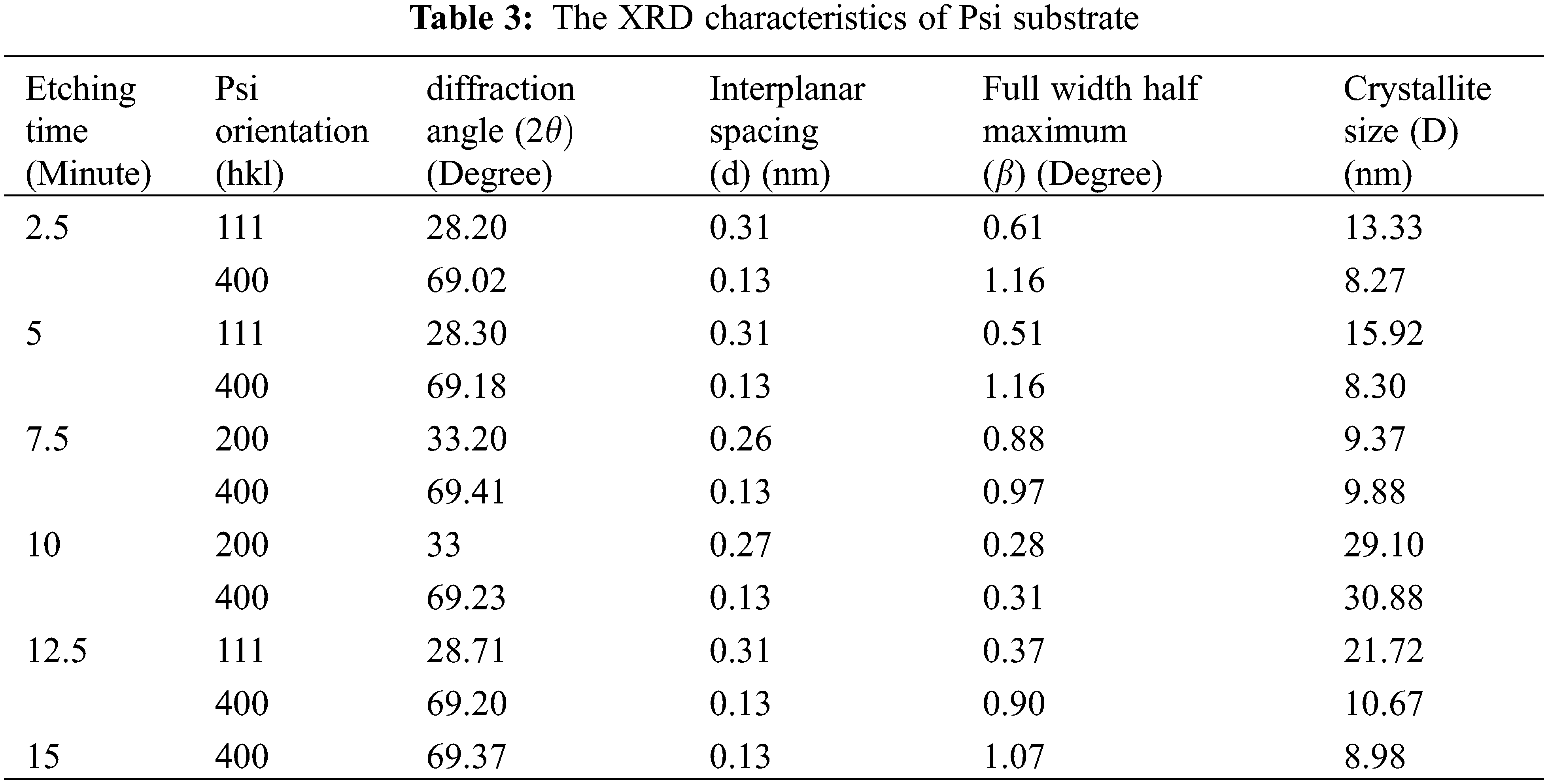
Fig. 5 shows an XRD pattern of GaN on Psi film that ranges from 20° to 70° (in 2

Figure 5: XRD pattern of the deposited GaN on Psi substrate

Fig. 6 shows the photoluminescence (PL) spectrum obtained from the prepared Psi substrates with the photoelectrochemical etching method at different etching times. The prepared Psi substrates exhibited yellow-orange visible PL with peak wavelengths in a range of 607–638 nm because of the surface states and the quantum confinement that developed on the Psi after the photoelectrochemical etching process as shown in Fig. 7 [56].

Figure 6: Room temperature photoluminescence of prepared Psi substrates by photoelectrochemical etching method assisted by laser at different etching time

Figure 7: Photoluminescence peak wavelength vs. etching time
The PL of Psi variant with the variation of etching time because PL intensity is affected the total volume of crystallites on the surface of Psi [57]. The energy gap was then calculated using Eq. (4) [58–60], where the Psi energy gap is definitely having higher energy gaps compared to Silicon (1.11 eV) and it increases from (1.94–2.1) eV as the etching time increases as shown in Fig. 8.
where:

Figure 8: Prepared porous silicon energy gap vs. etching time
h is Planck’s constant
c is the speed of light
λ is the peak wavelength of the photoluminescence of prepared Psi at different etching time
Notably, at the etching time of 10 min, the peak PL was observed at 589 nm, which fell in the yellow visible band [61].
According to Li et al. [62], the photoluminescence spectral of the prepared porous silicon substrate at the etching time of 10 mA/cm2 has been shifted after the deposition of GaN material on it due to the changes in the surface chemistry achieved.
Fig. 9 shows the PL spectrum obtained from GaN/Psi deposited at 1064 nm wavelength by the PLD method. Two PL peaks were observed after GaN/Psi was deposited, which fall in the ultraviolet (UV) band of 374 nm corresponding to GaN and in the infrared (IR) band of 730 nm corresponding to Psi.

Figure 9: Room temperature photoluminescence of the deposited GaN on Psi substrate by PLD method
Fig. 10 shows the 3D AFM images of Psi substrates with the photoelectrochemical etching method assisted by laser at different etching times for surface topography analysis. At the etching time of 2.5 min, pores began to form slightly on the surface with an oval shape of low height and did not cover all of the surfaces. As the etching time increased to 5 and 7 min, the pores on the surfaces had irregular distributions over the surface, oval shapes, and low heights. As the etching time reached 10 min, the pores formed homogeneously over the entire surface with a steeper oval shape.


Figure 10: 3D AFM images of prepared Psi substrates by photoelectrochemical etching method assisted by laser at different etching times
Furthermore, at etching times of 12.5 and 15 min, nonhomogenous pores started to dissociate. Root mean square height and surface roughness are provided in Table 5. Notably, the particle size distribution of the prepared Psi substrates was investigated at the nanometer range and at different etching times. Table 4 shows the AFM parameters prepared by Psi substrates at different etching times.

Fig. 11 shows a 3D AFM image of GaN deposited on the Psi layer with the PLD method for surface topography analysis. The GaN film had sharp oval particles with root means square (RMS) height and surface roughness of 17.49 and 4.83 nm, as shown in Table 6.

Figure 11: 3D AFM image and particle size distribution of GaN films deposited at 1064 nm laser wavelength

Fig. 12 shows FESEM images of the prepared Psi substrates at different etching times for surface morphology analysis. At etching times of 2.5 and 5 min, similar FESEM images were observed. The pores started to form on the surface. As the etching time increased to 10 min, dark pores with small diameters were observed, accompanied by uniformly distributed and homogeneous pores. Moreover, the cross-section of the FESEM image at 10 min displayed the thickness of the Psi layer to 36.02 nm.


Figure 12: FESEM and EDS images of prepared Psi substrates by photoelectrochemical etching method assisted by laser at different etching time
Furthermore, at etching times of 12.5 and 15 min, the pore diameters increased, and the pore walls were widened, leading to decreased number of pores on the surfaces of the prepared Psi substrates. The average diameters of the prepared Psi substrates at different etching times (2.5–15 min) were obtained from FESEM software images: 48.21, 66.23, 57.54, 49.02, 61.89, and 60.91 nm.
Moreover, the EDX spectrum of the prepared Psi substrates at different etching times was investigated to show the high peak of silicon.
Fig. 13 shows the FESEM image of GaN deposited on the Psi layer by the PLD method to investigate the surface morphology. The magnification of surface morphology of the GaN films was at 80,000× and 160,000×. The FESEM image showed that the average particle diameter was 51.88 nm. The GaN particle completed covered the Psi layer without voids or cracks, forming a uniform and homogeneous spherical particle size of 51.88 nm and showing cauliflower-like morphology.

Figure 13: FESEM images of GaN film deposited at the wavelength of 1064 nm, (A) Magnified 160,000×, (B) Magnified 80,000×, and (C) FESEM cross section that shows the thickness of GaN deposited Psi substrate
Also, through this examination, the thickness of the GaN nanostructures measured, which were deposited using the pulsed laser deposition technique, where it was found that the thickness of these films is approximately 117.4 nm, as presented in Fig. 13c.
The I–V characteristic of the prepared Psi substrate at an etching time of 10 min (Fig. 14A) was examined in the dark and under illumination by halogen light (100 mW/cm2 intensity) at room temperature. The current that passed through the Psi substrate increased with applied voltage because of an increase in the resistivity of the Psi layer [63]. Charge transfer created a depletion region in the prepared Psi near the electrical dipole, thereby causing a rectifying behavior [64].

Figure 14: Electrical characteristic of prepared Psi substrate under light and dark. (A) I–V characteristic, (B) C–V characteristic, (C) 1/C2 vs. voltage characteristic
As shown in Fig. 14B, C–V, the characteristic of prepared Psi substrate at an etching time of 10 min was examined at room temperature under an applied voltage of 0–3 V. The capacitance of the prepared Psi substrate decreased with increasing applied voltage. This effect was referred to as the increase in depletion region at increasing built-in potential [65,66].
As shown in Fig. 14C, 1/C2 vs. voltage characteristic of the prepared Psi substrate at an etching time of 10 min was investigated. A linear relation was observed between C2 and applied voltage. The potential built-in was determined by extrapolating the linear portion of the presented curve to a 1/C2 value of 0 points. The potential built-in was 0.34 eV.
As shown in Fig. 15, the I–V characteristic of GaN/Psi heterojunction in the dark and under illumination were examined under the following conditions: halogen light intensity of 100 mW/cm2, room temperature, and forward and reverse bias. The forward current increased with bias voltage because of the decrease in the depletion layer width. Moreover, the GaN/Psi film showed rectification characteristics, and the current transport mechanism in both layers was recombination tunneling [67,68].

Figure 15: I–V characteristic of GaN on Psi layer deposited by PLD method
As shown in Fig. 16, the C–V characteristic of the GaN/Psi film deposited at 1064 nm wavelength was examined under an applied voltage of 0–2 V. Capacitance decreased with increasing applied voltage because of the increase in the width of the depletion region and subsequent decrease in capacitance at the junction [69].

Figure 16: C–V characteristic of GaN films deposited at different laser wavelengths
Fig. 17 shows the 1/C2 and voltage characteristics of GaN films deposited at 1064 nm laser wavelength. The fabricated GaN on the Psi film was an abrupt junction, and the value of the built-in potential decreased from 0.34 to 0.31 eV after GaN was deposited at a laser wavelength of 1064 nm [70–74].

Figure 17: 1/C2–V characteristic of GaN films deposited at 1064 nm laser wavelength
High-performance GaN/Psi film was fabricated with a pulsed laser deposition method using 1064 nm Nd:YAG laser. A suitable Psi substrate was prepared with the photoelectrochemical etching method assisted by laser at different etching times. The prepared Psi substrate at 10 min of etching time had a high and crystallographic texture with PL at the yellow visible band and pores formed homogeneously over the entire surface. The GaN/Psi film displayed the high and hexagonal crystallographic texture in the (002) plane. The spectroscopic properties results revealed that the PL emission of the deposited nano-GaN films was in the ultraviolet band (374 nm) related to the GaN material and in the near-infrared band (730 nm) related to the Psi substrate. The topographical and morphological results of the GaN films confirmed that the deposited film had spherical grains with an average diameter of 51.8 nm and surface roughness of 4.8 nm. The GaN/Psi surface showed a cauliflower-like morphology. The built-in voltage decreased from 3.4 to 2.7 eV after deposition. The GaN/Psi film is a potential material ultraviolet optoelectronic device because of its high photosensitivity in the ultraviolet region.
Acknowledgement: The authors would like to thank the Laser and Optoelectronics Engineering Department/university of Technology for the logistic support of this work.
Funding Statement: The authors received no specific funding for this study.
Conflicts of Interest: The authors declare that they have no conflicts of interest to report regarding the present study.
References
1. Abdalla, S., Marzouki, F., Al-Ameer, S., Turkestani, S. (2013). Electric properties of n-GaN: Effect of different contacts on the electronic conduction. International Journal of Physics, 1, 41–48. [Google Scholar]
2. Khan, M. A. H., Rao, M. V. (2020). Gallium nitride (GaN) nanostructures and their gas sensing properties: A review. Sensors, 20(14), 3889. DOI 10.3390/s20143889. [Google Scholar] [CrossRef]
3. Amir, H. A. A. A., Fakhri, M. A., Alwahib, A. A. (2021). Review of GaN optical device characteristics, applications, and optical analysis technology. Materials Today: Proceedings, 42, 2815–2821. [Google Scholar]
4. Jorudas, J., Šimukovič, A., Dub, M., Sakowicz, M., Prystawko, P. et al. (2020). AlGaN/GaN on sic devices without a gan buffer layer: Electrical and noise characteristics. Micromachines, 11(12), 1131. DOI 10.3390/mi11121131. [Google Scholar] [CrossRef]
5. Koksaldi, O. S., Haller, J., Li, H., Romanczyk, B., Guidry, M. et al. (2018). N-polar GaN HEMTs exhibiting record breakdown voltage over 2000 V and low dynamic on-resistance. IEEE Electron Device Letters, 39(7), 1014–1017. DOI 10.1109/LED.2018.2834939. [Google Scholar] [CrossRef]
6. Jabbar, H. D., Fakhri, M. A., AbdulRazzaq, M. J. (2021). Gallium nitride–based photodiode: A review. Materials Today: Proceedings, 42, 2829–2834. [Google Scholar]
7. Choi, U., Kim, H. S., Lee, K., Jung, D., Kwak, T. et al. (2020). Direct current and radio frequency characterizations of AlGaN/AlN/GaN/AlN double-heterostructure high-electron mobility transistor (DH-HEMT) on sapphire. Physica Status Solidi, 217(7), 1900695. DOI 10.1002/pssa.201900695. [Google Scholar] [CrossRef]
8. Dalla Vecchia, M., Ravyts, S., Van den Broeck, G., Driesen, J. (2019). Gallium-nitride semiconductor technology and its practical design challenges in power electronics applications: An overview. Energies, 12(14), 2663. DOI 10.3390/en12142663. [Google Scholar] [CrossRef]
9. Denbaars, S. P. (1997). Gallium-nitride-based materials for blue to ultraviolet optoelectronics devices. Proceedings of the IEEE, 85(11), 1740–1749. DOI 10.1109/5.649651. [Google Scholar] [CrossRef]
10. Justice, J., Kadiyala, A., Dawson, J., Korakakis, D. (2013). Group III-nitride based electronic and optoelectronic integrated circuits for smart lighting applications. MRS Online Proceedings Library, 1492, 123–128. DOI 10.1557/opl.2013.369. [Google Scholar] [CrossRef]
11. Chandrasekar, H., Uren, M. J., Eblabla, A., Hirshy, H., Casbon, M. A. et al. (2018). Buffer-induced current collapse in GaN HEMTs on highly resistive Si substrates. IEEE Electron Device Letters, 39(10), 1556–1559. DOI 10.1109/LED.55. [Google Scholar] [CrossRef]
12. Ben, J., Liu, X., Wang, C., Zhang, Y., Shi, Z. et al. (2021). 2D III-nitride materials: Properties, growth, and applications. Advanced Materials, 33(27), 2006761. DOI 10.1002/adma.202006761. [Google Scholar] [CrossRef]
13. Liu, L., Yang, C., Patanè, A., Yu, Z., Yan, F. et al. (2017). High-detectivity ultraviolet photodetectors based on laterally mesoporous GaN. Nanoscale, 9(24), 8142–8148. DOI 10.1039/C7NR01290J. [Google Scholar] [CrossRef]
14. Romanczyk, B., Zheng, X., Guidry, M., Li, H., Hatui, N. et al. (2020). W-band power performance of SiN-passivated N-polar GaN deep recess HEMTs. IEEE Electron Device Letters, 41(3), 349–352. DOI 10.1109/LED.55. [Google Scholar] [CrossRef]
15. Alshahed, M., Heuken, L., Alomari, M., Cora, I., Toth, L. et al. (2018). Low-dispersion, high-voltage, low-leakage GaN HEMTs on native GaN substrates. IEEE Transactions on Electron Devices, 65(7), 2939–2947. DOI 10.1109/TED.2018.2832250. [Google Scholar] [CrossRef]
16. SaifAddin, B. K., Almogbel, A. S., Zollner, C. J., Wu, F., Bonef, B. et al. (2020). Algan deep-ultraviolet light-emitting diodes grown on SiC substrates. ACS Photonics, 7(3), 554–561. DOI 10.1021/acsphotonics.9b00600. [Google Scholar] [CrossRef]
17. Pashnev, D., Kaplas, T., Korotyeyev, V., Janonis, V., Urbanowicz, A. et al. (2020). Terahertz time-domain spectroscopy of two-dimensional plasmons in AlGaN/GaN heterostructures. Applied Physics Letters, 117(5), 051105. DOI 10.1063/5.0014977. [Google Scholar] [CrossRef]
18. Jakštas, V., Jorudas, J., Janonis, V., Minkevičius, L., Kašalynas, I. et al. (2018). Development of AlGaN/GaN/SiC high-electron-mobility transistors for THz detection. Lithuanian Journal of Physics, 58(2). DOI 10.3952/physics.v58i2.3748. [Google Scholar] [CrossRef]
19. Selvaraj, S. L., Suzue, T., Egawa, T. (2009). Breakdown enhancement of AlGaN/GaN HEMTs on 4-in silicon by improving the GaN quality on thick buffer layers. IEEE Electron Device Letters, 30(6), 587–589. DOI 10.1109/LED.2009.2018288. [Google Scholar] [CrossRef]
20. Sai, P., Jorudas, J., Dub, M., Sakowicz, M., Jakštas, V. et al. (2019). Low frequency noise and trap density in GaN/AlGaN field effect transistors. Applied Physics Letters, 115(18), 183501. DOI 10.1063/1.5119227. [Google Scholar] [CrossRef]
21. Abdul Amir, H. A. A., Fakhri, M. A., Alwahib, A. A., Salim, E. T., Alsultany, F. H. et al. (2022). An investigation on GaN/porous-Si NO2 gas sensor fabricated by pulsed laser ablation in liquid. Sensors and Actuators B: Chemical, 367(2022), 132163. DOI 10.1016/j.snb.2022.132163. [Google Scholar] [CrossRef]
22. Poblenz, C., Waltereit, P., Rajan, S., Heikman, S., Mishra, U. K. et al. (2004). Effect of carbon doping on buffer leakage in AlGaN/GaN high electron mobility transistors. Journal of Vacuum Science & Technology B: Microelectronics and Nanometer Structures Processing, Measurement, and Phenomena, 22(3), 1145–1149. DOI 10.1116/1.1752907. [Google Scholar] [CrossRef]
23. Ogugua, S. N., Ntwaeaborwa, O. M., Swart, H. C. (2020). Latest development on pulsed laser deposited thin films for advanced luminescence applications. Coatings, 10(11), 1078. DOI 10.3390/coatings10111078. [Google Scholar] [CrossRef]
24. Abdul Amir, H. A. A., Fakhri, M. A., Alwahib, A. A., Salim, E. T., Alsultany, F. H. et al. (2022). Synthesis of gallium nitride nanostructure using pulsed laser ablation in liquid for photoelectric detector. Materials Science in Semiconductor Processing, 150, 106911. DOI 10.1016/j.mssp.2022.106911. [Google Scholar] [CrossRef]
25. Li, G., Wang, W., Yang, W., Wang, H. (2015). Epitaxial growth of group III-nitride films by pulsed laser deposition and their use in the development of LED devices. Surface Science Reports, 70(3), 380–423. DOI 10.1016/j.surfrep.2015.06.001. [Google Scholar] [CrossRef]
26. Al-Jumaili, B. E. B., Talib, Z. A., Ramizy, A., Aljameel, A., Baqiah, H. et al. (2021). Formation and photoluminescence properties of porous silicon/copper oxide nanocomposites fabricated via electrochemical deposition technique for photodetector application. Digest Journal of Nanomaterials and Biostructures, 16(1), 297–310. [Google Scholar]
27. Abdul Amir, H. A. A., Fakhri, M. A., Alwahib, A. A., Salim, E. T. (2022). Optical investigations of GaN deposited nano films using pulsed laser ablation in ethanol. International Journal of Nanoelectronics and Materials, 15(2), 129–138. [Google Scholar]
28. Saverina, E. A., Zinchenko, D. Y., Farafonova, S. D., Galushko, A. S., Novikov, A. A. et al. (2020). Porous silicon preparation by electrochemical etching in ionic liquids. ACS Sustainable Chemistry & Engineering, 8(27), 10259–10264. DOI 10.1021/acssuschemeng.0c03133. [Google Scholar] [CrossRef]
29. Kang, X., Wu, L., Xu, J., Liu, D., Song, Q. et al. (2020). Preparation and photoelectrochemical properties of porous silicon/carbon dots composites. IOP Conference Series: Materials Science and Engineering, 892(1), 012025. DOI 10.1088/1757-899X/892/1/012025. [Google Scholar] [CrossRef]
30. Abdulrahman, A. F., Ahmed, S. M., Barzinjy, A. A., Hamad, S. M., Ahmed, N. M. et al. (2021). Fabrication and characterization of high-quality UV photodetectors based ZnO nanorods using traditional and modified chemical bath deposition methods. Nanomaterials, 11(3), 677. DOI 10.3390/nano11030677. [Google Scholar] [CrossRef]
31. Alia, A. M., Mohammedb, A. S., Hanfooshb, S. M. (2021). The spectral responsivity enhancement for gallium-doped CdO/PS heterojunction for UV detector. Journal of Ovonic Research, 17(3), 239–245. [Google Scholar]
32. Salim, E. T. (2013). Surface morphology and X-ray diffraction analysis for silicon nanocrystal-based heterostructures. Surface Review and Letters, 20(5), 1350046. DOI 10.1142/S0218625X13500467. [Google Scholar] [CrossRef]
33. Hadi, H. A., Ismail, R. A., Habubi, N. F. (2013). Fabrication and characterization of porous silicon layer prepared by photo-electrochemical etching in CH3OH: HF solution. International Letters of Chemistry, Physics and Astronomy, 3, 29–36. [Google Scholar]
34. Dubey, R. S., Gautam, D. K. (2011). Porous silicon layers prepared by electrochemical etching for application in silicon thin film solar cells. Superlattices and Microstructures, 50(3), 269–276. DOI 10.1016/j.spmi.2011.07.003. [Google Scholar] [CrossRef]
35. Ismail, R. A., Alwan, A. M., Ahmed, A. S. (2017). Preparation and characteristics study of nano-porous silicon UV photodetector. Applied Nanoscience, 7(1), 9–15. DOI 10.1007/s13204-016-0544-9. [Google Scholar] [CrossRef]
36. Xu, J., Liu, S., Yang, Y., Li, J., Tian, C. et al. (2019). Preparation of porous silicon by electrochemical etching methods and its morphological and optical properties. International Journal of Electrochemical Science, 5188–5199. DOI 10.20964/2019.06.10. [Google Scholar] [CrossRef]
37. Moretta, R., de Stefano, L., Terracciano, M., Rea, I. (2021). Porous silicon optical devices: Recent advances in biosensing applications. Sensors, 21(4), 1336. DOI 10.3390/s21041336. [Google Scholar] [CrossRef]
38. Chen, J. T., Bergsten, J., Lu, J., Janzén, E., Thorsell, M. et al. (2018). A GaN–SiC hybrid material for high-frequency and power electronics. Applied Physics Letters, 113(4), 041605. DOI 10.1063/1.5042049. [Google Scholar] [CrossRef]
39. Saxena, S. K., Sahu, G., Kumar, V., Sahoo, P. K., Sagdeo, P. R. et al. (2015). Effect of silicon resistivity on its porosification using metal induced chemical etching: Morphology and photoluminescence studies. Materials Research Express, 2(3), 036501. DOI 10.1088/2053-1591/2/3/036501. [Google Scholar] [CrossRef]
40. Hassan, M. M., Fakhri, M. A., Adnan, S. A. (2019). 2-D of nano photonic silicon fabrication for sensing application. Digest Journal of Nanomaterials and Biostructures, 14(4), 873–878. [Google Scholar]
41. Fakhri, M. A., AbdulRazzaq, M. J., Alwahib, A. A., Muttlak, W. H. (2020). Theoretical study of a pure LiNbO3/Quartz waveguide coated gold nanorods using supercontinuum laser source. Optical Materials, 109, 110363. DOI 10.1016/j.optmat.2020.110363. [Google Scholar] [CrossRef]
42. Ismail, R. A., Rasheed, B. G., Salm, E. T., Al-Hadethy, M. (2007). Transparent and conducting ZnO films prepared by reactive pulsed laser deposition. Journal of Materials Science: Materials in Electronics, 18(4), 397–400. [Google Scholar]
43. Sun, Y., Wu, D., Liu, K., Zheng, F. (2019). Colossal permittivity and low dielectric loss of thermal oxidation single-crystalline Si wafers. Materials, 12, 1102. DOI 10.3390/ma12071102. [Google Scholar] [CrossRef]
44. Abdul-Hamead, A. A., Othman, F. M., Fakhri, M. A. (2021). Preparation of MgO–MnO2 nanocomposite particles for cholesterol sensors. Journal of Materials Science: Materials in Electronics, 32(11), 15523–15532. [Google Scholar]
45. Mohsin, M. H., Numan, N. H., Salim, E. T., Fakhri, M. A. (2021). Physical properties of sic nanostructure for optoelectronics applications. Journal of Renewable Materials, 9(9), 1519–1530. DOI 10.32604/jrm.2021.015465. [Google Scholar] [CrossRef]
46. Sampath, S., Maydannik, P., Ivanova, T., Shestakova, M., Homola, T. et al. (2016). Efficient solar photocatalytic activity of TiO2 coated nano-porous silicon by atomic layer deposition. Superlattices and Microstructures, 97, 155–166. DOI 10.1016/j.spmi.2016.06.004. [Google Scholar] [CrossRef]
47. Ismail, R. A., Salim, E. T., Hamoudi, W. K. (2013). Characterization of nanostructured hydroxyapatite prepared by Nd:YAG laser deposition. Materials Science and Engineering C, 33(1), 47–52. DOI 10.1016/j.msec.2012.08.002. [Google Scholar] [CrossRef]
48. Jabbar, H. D., Fakhri, M. A., AbdulRazzaq, M. J. (2022). Synthesis gallium nitride on porous silicon nano-structure for optoelectronics devices. Silicon, 2022. DOI 10.1007/s12633-022-01999-8. [Google Scholar] [CrossRef]
49. Lu, J., Chen, J. T., Dahlqvist, M., Kabouche, R., Medjdoub, F. et al. (2019). Transmorphic epitaxial growth of AlN nucleation layers on SiC substrates for high-breakdown thin GaN transistors. Applied Physics Letters, 115(22), 221601. DOI 10.1063/1.5123374. [Google Scholar] [CrossRef]
50. Fakhri, M. A., Salim, E. T., Abdulwahhab, A. W., Hashim, U., Munshid, M. A. et al. (2019). The effect of annealing temperature on optical and photoluminescence properties of LiNbO3. Surface Review and Letters, 26(10), 1950068. DOI 10.1142/S0218625X19500689. [Google Scholar] [CrossRef]
51. Alwazny, M. S., Ismail, R. A., Salim, E. T. (2022). High-quantum efficiency of Au@LiNbO3 core–shell nano composite as a photodetector by two-step laser ablation in liquid. Applied Physics A, 128, 500. DOI 10.1007/s00339-022-05651-5. [Google Scholar] [CrossRef]
52. Chen, D. Y., Malmros, A., Thorsell, M., Hjelmgren, H., Kordina, O. et al. (2020). Microwave performance of ‘buffer-free’ GaN-on-SiC high electron mobility transistors. IEEE Electron Device Letters, 41(6), 828–831. [Google Scholar]
53. Al-Douri, Y., Fakhri, M. A., Bouhemadou, A., Khenata, R., Ameri, M. (2018). Stirrer time effect on optical properties of nanophotonic LiNbO3. Materials Chemistry and Physics, 203, 243–248. DOI 10.1016/j.matchemphys.2017.10.024. [Google Scholar] [CrossRef]
54. Abood, M. K., Salim, E. T., Saimon, J. A., Hadi, A. A. (2021). Electrical conductivity, mobility and carrier concentration in Nb2O5 films: Effect of NH4OH molarity. International Journal of Nanoelectronics and Materials, 14(3), 259–268. [Google Scholar]
55. Kang, B. K., Song, Y. H., Kang, S. M., Choi, Y. C., Lee, D. K. et al. (2011). Formation of highly efficient dye-sensitized solar cells by effective electron injection with GaN nanoparticles. Journal of the Electrochemical Society, 158(7), H693. DOI 10.1149/1.3583505. [Google Scholar] [CrossRef]
56. Libon, I. H. (2002). Quantum confinement in porous silicon in the effective-mass limit. In: Ultrafast dynamics of quantum systems, pp. 690–690. Boston, MA: Springer. [Google Scholar]
57. Kim, D. A., Shim, J. H., Cho, N. H. (2004). PL and EL features of p-type porous silicon prepared by electrochemical anodic etching. Applied Surface Science, 234, 256–261. DOI 10.1016/j.apsusc.2004.05.028. [Google Scholar] [CrossRef]
58. Salim, E. T., Al Wazny, M. S., Fakhry, M. A. (2013). Glancing angle reactive pulsed laser deposition (GRPLD) for Bi2O3/Si heterostructure. Modern Physics Letters B, 27(16), 1350122. DOI 10.1142/S0217984913501224. [Google Scholar] [CrossRef]
59. Salim, E. T., Saimon, J. A., Abood, M. K., Fakhri, M. A. (2020). Effect of silicon substrate type on Nb2O5/Si device performance: An answer depends on physical analysis. Optical and Quantum Electronics, 52(10), 463. DOI 10.1007/s11082-020-02588-y. [Google Scholar] [CrossRef]
60. Awayiz, M. T., Salim, E. T. (2020). Photo voltaic properties of Ag2O/Si heterojunction device: Effect of substrate conductivity. Materials Science Forum, 1002, 200–210. DOI 10.4028/www.scientific.net/MSF.1002.200. [Google Scholar] [CrossRef]
61. Ouellette, R. J., Rawn, J. D. (2018). Organic chemistry: Structure, mechanism, synthesis. 2nd Edition. Academic Press. [Google Scholar]
62. Li, K. H., Tsai, C., Sarathy, J., Campbell, J. C. (1993). Chemically induced shifts in the photoluminescence spectra of porous silicon. Applied Physics Letters, 62(24), 3192–3194. DOI 10.1063/1.109126. [Google Scholar] [CrossRef]
63. Canham, L. (2014). Handbook of porous silicon, pp. 163–170. Berlin, Germany: Springer International Publishing. [Google Scholar]
64. Swanson, W. E. (1960). Tables for conversion of X-ray diffraction angles to in-terplanar spacing. National Bureau of Standards. [Google Scholar]
65. Muhsien, M. A., Salim, E. T., Agool, I. R. (2013). Preparation and characterization of (Au/n-SnO2/SiO2/Si/Al) MIS device for optoelectronic application. International Journal of Optics, 2013, 756402. DOI 10.1155/2013/756402. [Google Scholar] [CrossRef]
66. Wang, T., Lia, X., Feng, W., Lid, W., Taod, C. et al. (2011). Structure and photoluminescence properties of the quasi-regular arrangements of porous silicon. Optoelectronics and Advanced Materials-Rapid Communications, 5, 495–498. [Google Scholar]
67. Narang, K., Bag, R. K., Singh, V. K., Pandey, A., Saini, S. K. et al. (2020). Improvement in surface morphology and 2DEG properties of AlGaN/GaN HEMT. Journal of Alloys and Compounds, 815, 152283. DOI 10.1016/j.jallcom.2019.152283. [Google Scholar] [CrossRef]
68. Yang, C., Luo, X., Sun, T., Zhang, A., Ouyang, D. et al. (2019). High breakdown voltage and low dynamic ON-resistance AlGaN/GaN HEMT with fluorine ion implantation in SiNx passivation layer. Nanoscale Research Letters, 14(1), 1–6. DOI 10.1186/s11671-019-3025-8. [Google Scholar] [CrossRef]
69. Abd, A. N., Habubi, N. F., Reshak, A. H., Mansour, H. L. (2018). Enhancing the electrical properties of porous silicon photodetector by depositing MWCNTs. International Journal of Nanoelectronics & Materials, 11(3), 241–248. [Google Scholar]
70. Ismail, R. A., Hasan, N., Shaker, S. S. (2022). Preparation of Bi2Sr2CaCu2Ox thin film by pulsed laser deposition for optoelectronic devices application. Silicon, 14(6), 2625–2633. DOI 10.1007/s12633-021-01061-z. [Google Scholar] [CrossRef]
71. Hassan, M. A. M., Al-Kadhemy, M. F. H., Salem, E. T. (2014). Effect irradiation time of gamma ray on MSISM (Au/SnO2/SiO2/Si/Al) devices using theoretical modeling. International Journal of Nanoelectronics and Materials, 8(2), 69–82. [Google Scholar]
72. Ismail, R. A., Mousa, A. M., Khashan, K. S., Mohsin, M. H., Hamid, M. K. (2016). Synthesis of PbI2 nanoparticles by laser ablation in methanol. Journal of Materials Science: Materials in Electronics, 27(10), 10696–10700. [Google Scholar]
73. Hussein, B. H., Mahdi, S. H., Makki, S. A., Al-Maiyaly, B. K. (2019). Synthesis and study the structure, electrical and optical properties of Bi2−xCdxSr2Ca2Cu3O10+δ thin film superconductors. Energy Procedia, 157, 100–110. DOI 10.1016/j.egypro.2018.11.169. [Google Scholar] [CrossRef]
74. Fakhri, M. A., Basheer, R. A., Banoosh, A. M., Azeez, H. N. (2021). Rapid thermal oxidation of nano silver film for solar cell fabrication. Digest Journal of Nanomaterials & Biostructures, 16(2), 367–375. [Google Scholar]
Cite This Article
 Copyright © 2023 The Author(s). Published by Tech Science Press.
This work is licensed under a Creative Commons Attribution 4.0 International License , which permits unrestricted use, distribution, and reproduction in any medium, provided the original work is properly cited.
 Downloads
 Citation Tools