
 Submit a Paper
 Propose a Special lssue
 Open Access
ARTICLE

Passivation of PEA+ to CsPbI3 (110) Surface States: From the First Principles Calculations
1
School of Materials Science and Engineering, State Key Laboratory of Advanced Processing and Recycling of Nonferrous Metals,
Lanzhou University of Technology, Lanzhou, 730050, China
2
Department of Materials Engineering, Lanzhou Institute of Technology, Lanzhou, 730050, China
3
School of Peili Mechanical Engineering, Lanzhou City College, Lanzhou, 730070, China
4
School of Chemical Engineering, Northwest University, Xi’an, 710069, China
* Corresponding Author: Fuling Tang. Email:
(This article belongs to the Special Issue: Perovskite Solar Cells)
Journal of Renewable Materials 2023, 11(3), 1293-1301. https://doi.org/10.32604/jrm.2022.023095
Received 09 April 2022; Accepted 10 May 2022; Issue published 31 October 2022
 View Full Text
 Download PDF
Abstract
This work investigates the effect of passivation on the electronic properties of inorganic perovskite CsPbI3 materials by using first-principles calculations with density functional theory (DFT). The passivation effect after the addition of Phenylethylamine (PEA+ ) molecule to CsPbI3 (110) surface is studied. The results of density of states (DOS) calculations show that the CsPbI3 (110) surface model with I atom terminated reveals new electronic DOS peaks (surface states) near the Fermi level. These surface states are mainly due to the contribution of I-5p orbital and are harmful to the CsPbI3-based solar cells because they reduce the photoelectric conversion efficiency. The surface states near the Fermi level are significantly reduced, and the decline rate reaches 38.8% with the addition with PEA+ molecule to the CsPbI3 (110) surface.Graphic Abstract
Keywords
After more than ten years of development, perovskite solar cells (PSCs) have made amazing progress, whereas how to further increase device stability and efficiency of PSCs is still a matter of concern. Since the perovskite crystal growth requires high temperature and the crystallization is very fast, the existence of defects in the polycrystalline perovskite prepared by the solution method is inevitable, and it is harmful to the performance of the devices. How to passivate the defects of the perovskite absorber layer is very important to improve the performance of the device, which is of great significance for the mechanism research and further development of PSCs [1–3].
According to the type and location of the defect states, many methods have been adopted to reduce the defect effects in the body, grain boundary and surface of the perovskite layer. The defects in the perovskite form shallow level defect states and deep level defect states between the band gaps of the perovskite, which affect the transport behavior of carriers and reduce the efficiency of the device. At the same time, defects act as channels for ion migration, causing the hysteresis of PSCs. In addition, the water and oxygen molecules in the air enter the perovskite layer through the defect position. This promotes the decomposition of the perovskite, which does harm to the stability of the device. For the sake of further improving the efficiency and stability of the PSCs, passivating the defect states of the perovskite is a very effective method [4,5].
In recent years, in order to passivate the perovskite grain boundary or surface defects, various types of additives have been introduced into the perovskite. These additives can bond at the perovskite defect position to achieve the passivation effect [6–13]. Halwidl et al. studied the formation of the first monolayer of water at the (001) surfaces of Srn+1RunO3n+1 (n = 1, 2) and found the modification of the structural parameters, which was successful in tuning the electrical and magnetic properties of perovskites. It also was instrumental in adjusting the surface chemistry and reactivity of these promising materials [14]. Fu et al. [7] used lead pyridine dicarboxylate (PbPyA2) as a perovskite additive, and they found that the pyridine group and carboxylic acid group of PbPyA2 can interact strongly with the ions of the perovskite to form high-quality perovskite grains and passivate the grain boundary defects, and the defect states density reduced from 1.35 × 1016 cm−3 to 8.83 × 1015 cm−3, and the efficiency increased from 18.86% to 19.96%. Yang et al. used imidazole sulfonate zwitterion, 4-(1H-imidazol-3-ium-3-yl) butane-1-sulfonate (IMS) as an additive to passivate I− ions defects, then the efficiency increased from 18.77% to 20.84%, and the open-circuit voltage (Voc) increased from 1.103 to 1.208 V [12]. There are also many other materials, such as small molecules, halogenated organic salts, polymers, ionic liquids, etc. that have been applied to the surface layer of perovskite modification [15–22]. The Grätzel group used poly (methyl methacrylate) (PMMA) polymer template method as a nucleation site to regulate the growth of perovskite, and reduce the defects of perovskite effectively, finally obtain a certification efficiency of 21.02% [23]. The Seok group introduced I3− ions in the two-step method and found that they can passivate the deep-level defects of perovskite and increased the device efficiency to 22.1% [24]. You research team used phenethylammonium iodide (PEAI) to passivate the perovskite material surface, inhibiting the recombination of carriers, and the certification efficiency reached to 23.3% [25]. Wang group used PEA+ molecule to modify the surface of CsPbI3 and found that the organic cation surface terminated α-CsPbI3 perovskite not only shows moisture resistance and enhanced phase stability, but also exhibits passivated effects with higher Voc and fill factor (FF) [26]. But they did not clarify the microscopic mechanism of this phenomenon. Because of this, low-index surfaces of CsPbI3 have been researched in this work. We investigated and calculated these surfaces separately, and the results show that there are surface states on the (110) surface. Next, we examine the passivation effect of PEA+ molecule to the surface states of CsPbI3 (110) and explore the microscopic mechanism after modification by the first-principles calculations.
Our calculation works are performed using first-principles calculations based on the generalized gradient approximation (GGA) of the density functional theory (DFT) generalized in the Vienna ab-initio simulation package (VASP) [27,28]. Projection-adding plane wave (PAW) is used to describe the atomic pseudopotential, and Perdew-Burke-Ernzerh (PBE) is used to describe exchange correlation energy [29,30]. The passivation model is established by using PEA+ to adsorb on CsPbI3 (110) surface. The electronic configurations of H, N, C, Cs, I and Pb atoms in the crystal model are H1s1, N2s22p3, C2s22p2, [Xe]6s1, [Kr]5s25p5 and [Xe]5d106s26p2. The cut-off energy is 340 eV in the calculation of the system. The k-point meshing of Brillouin region of CsPbI3 (110) surface and PEA+-CsPbI3 (110) system is the same as 4 × 3 × 1. The passivation model structure is shown in Fig. 1, the right is the adsorbed PEA+ molecule, and the relaxed CsPbI3 (110) plane with 7 atomic layers on the left. In order to avoid atomic interaction between adjacent periodic units along the Z axis, we added a 20 Å vacuum layer to the adsorption system. During the relaxation of the structure, the three-layer atoms which are far away from surface CsPbI3 are fixed at the left end, and the remaining atoms and PEA+ molecule are released. The passivation system contains 3 Cs atoms, 3 Pb atoms and 11 I atoms, and a passivation molecule. The lattice parameters of the passivation system are a = 6.41 Å, b = 9.06 Å, and c = 28.59 Å. The force convergence accuracy and energy convergence accuracy are set to 5 × 10⁻² eV/Å and 10−5 eV, respectively, and the calculation results can meet the accuracy requirements.
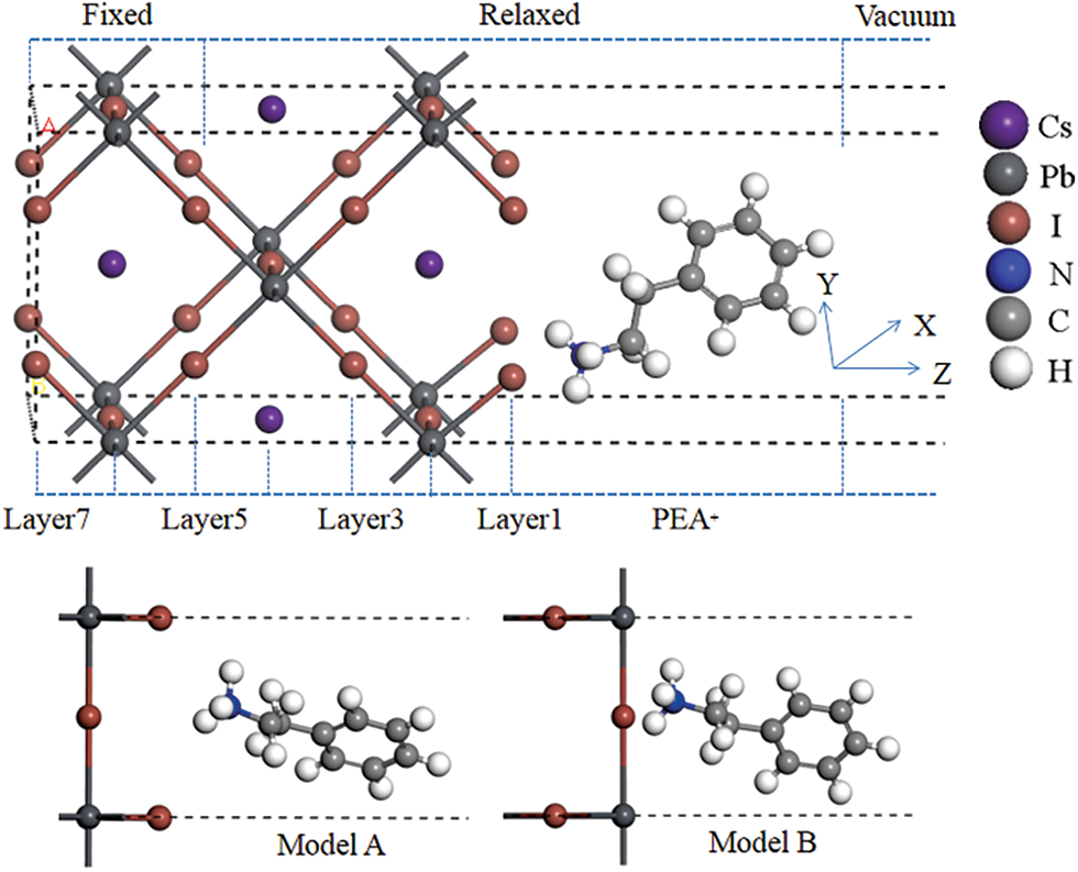
Figure 1: Architecture of PEA+-CsPbI3 adsorption system
3.1 Adsorption Structure and Energy of PEA+-CsPbI3 System
The PEA+-CsPbI3 passivation structure has two different binding methods: I (layer 1) is used as the end face to combine with PEA+ molecule, and the I-Pb-Cs (layer 2) is used as the end face to combine with PEA+ molecule. For the convenience of explanation, we call these two different combinations as model A and model B (as shown in Fig. 1), respectively. The interface distance d of the adsorption system is defined as the shortest distance between H atoms in PEA+ molecule and I atoms in the perovskite surface. According to this definition, the optimal passivation distance can be obtained by using the single-point energy calculation method. After many tests, it is found that when the interface distances are 3.72 and 3.11 Å, model A and model B reach the lowest point of total interface energy, respectively (as shown in Fig. 2). The stability of the passivation system can be evaluated by the adsorption energy, that is, when the adsorption energy value is negative, the system can be considered stable [31]. The adsorption energy of PEA+-CsPbI3 passivation structure is derived by using the following formula (1) [32,33].
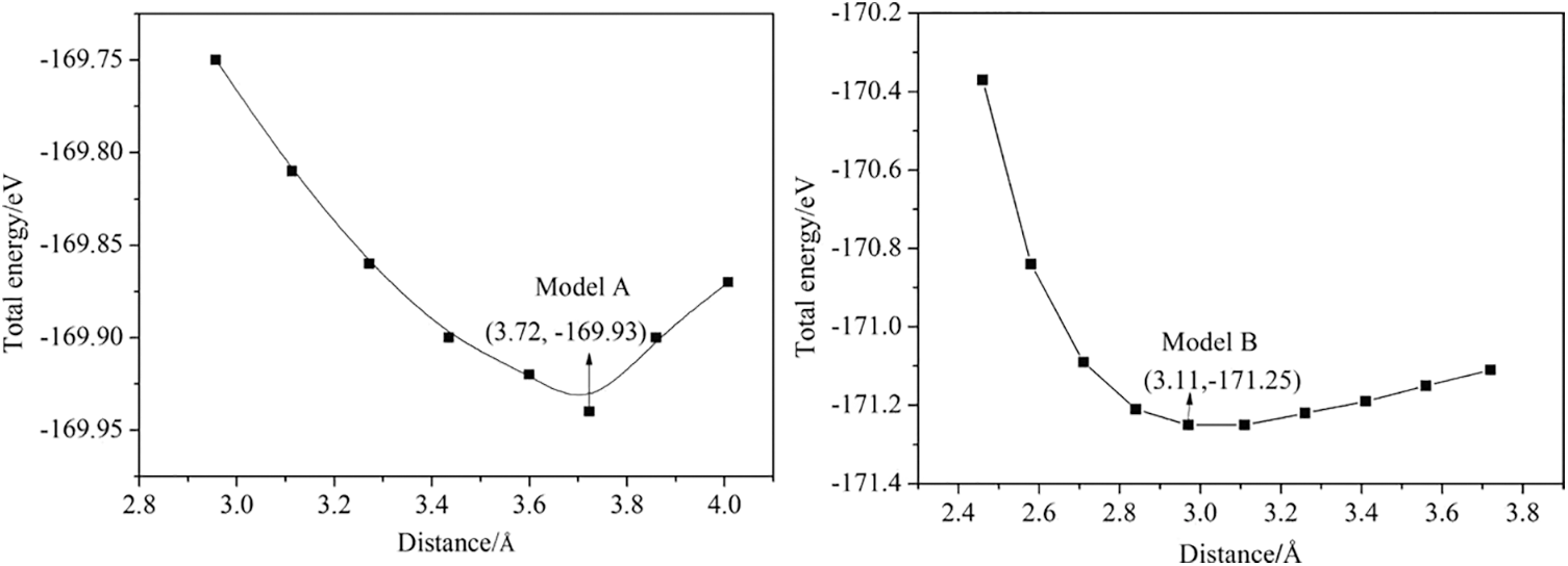
Figure 2: Variation of PEA+-CsPbI3 system energy with adsorption distance
In this expression (1), where Eatom/CsPbI3 and ECsPbI3 are the total energy of the adsorption system and surface CsPbI3 (110), respectively. The total energy of the adsorbed material PEA+ molecule is Eatom, where N = 1 means adsorbing one molecule. The calculation results show that the adsorption energies of model A and model B are −3.37 eV (each PEA+ molecule) and −0.43 eV (each PEA+ molecule), respectively, it can be seen from the calculation results that model A is more stable than model B. Therefore, the electronic properties of model A are studied in the subsequent calculation.
3.2 Electronic Properties of CsPbI3 (110) Surface and PEA+-CsPbI3 System
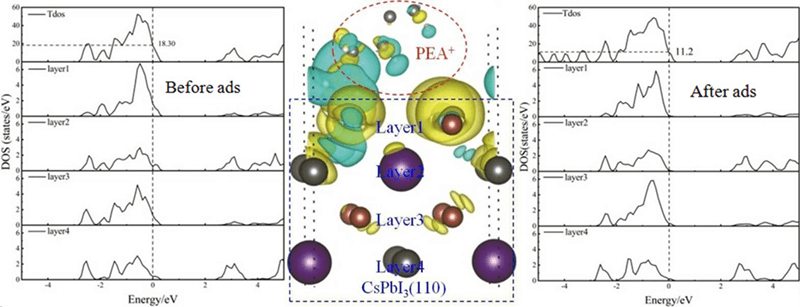
The total density of states (TDOS) of the clean surface CsPbI3 (110), and the local density of states (LDOS) of layers 1 to 7, and the partial density of states (PDOS) of the first layer are shown in Fig. 3. The 1st, 3rd, 5th, and 7th layers, each of which is occupied by only the same number of I atoms, and the 2nd, 4th, and 6th layers are occupied by the same type and number atoms in each layer, which are Cs, Pb and I atoms. In the surface model, released layers are the first to fourth layers, and fixed layers are the fifth to seventh layers. By comparing DOS of each layer, it can be found that the LDOS in the first and seventh layers are similar, and their contribution to the surface states is the largest at the Fermi level, which is mainly due to the contribution of unsaturated bonds at the end faces. From the 2nd to the 6th layer, every layer contributes to the surface states at the Fermi level, but the contribution to the surface states is smaller than that of layer 1 and layer 7. Through the analysis of PDOS, it is found that the contribution of I-5p orbital to the surface states is the most. Here, we only give the PDOS of the first layer atoms. The surface states act as the recombination center for photogenerated carriers, and shorten the lifetime of the carriers, increase the recombination loss of radiation, and ultimately reduce the optoelectronic performance of the device. The calculation results show that some surface states appear on the clean surface CsPbI3 (110), which may have a detrimental effect on the optoelectronic properties of the device. Therefore, it is particularly important to find a surface passivation substance to weaken or even eliminate the surface states.
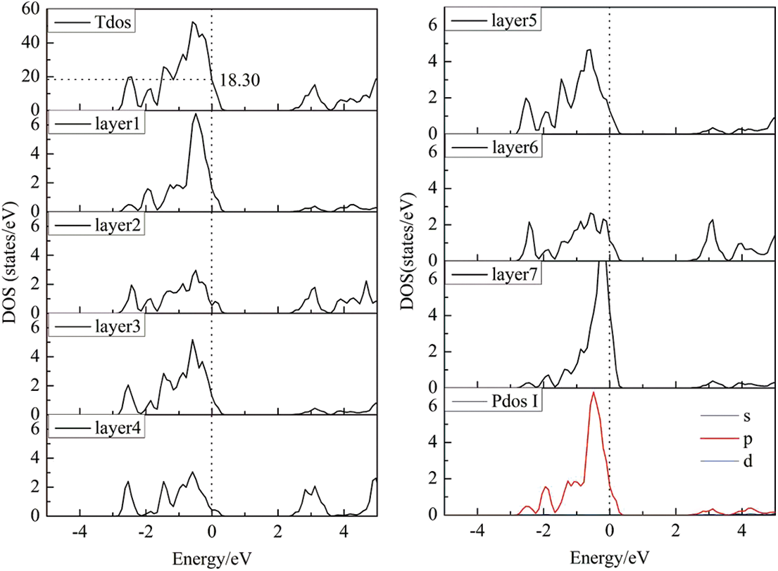
Figure 3: Density of states of clean surface CsPbI3 (110)
Fig. 4 shows the DOS of the PEA+-CsPbI3 passivation system. From the TDOS, it can be found that the adsorption of PEA+ greatly weakens the surfaces states of surface CsPbI3 (110). Compared with that of before passivation, its value has reduced from 18.3 to 11.2 (relative value), and the passivation rate is 38.8%. In addition, the band gap of surface CsPbI3 (110) is regulated by PEA+, compared with that of clean surface CsPbI3 (110), the surface band gap value of the PEA+-CsPbI3 passivation system will increase from 0.98 eV to about 1.06 eV. From the Fig. 4, it can be seen that the addition of passivation substances reduces the surface states significantly, especially in the first layer to the fourth layer, the electronic states at the Fermi level is almost zero. The passivation effect of layers 5 to 7 is not obvious because they are far away from passivation substances. From the DOS of the passivation material PEA+, it can be seen that there are no electronic states near the Fermi level, indicating that the material is an ideal passivation material. From the PDOS of the I atom of the first layer, it can be seen that the electronic states of the I-5p orbital at the Fermi level is almost zero, and the passivation effect is very ideal. Through the above analysis, it is found that the electronic states of PEA+-CsPbI3 system in the vicinity of Fermi level mainly originate from unsaturated bonds. To sum up, the calculation results show that PEA+ substance can reduce and eliminate the surface states of the CsPbI3 (110) surface. The passivation effect of PEA+ to the CsPbI3 (110) surface is effective.
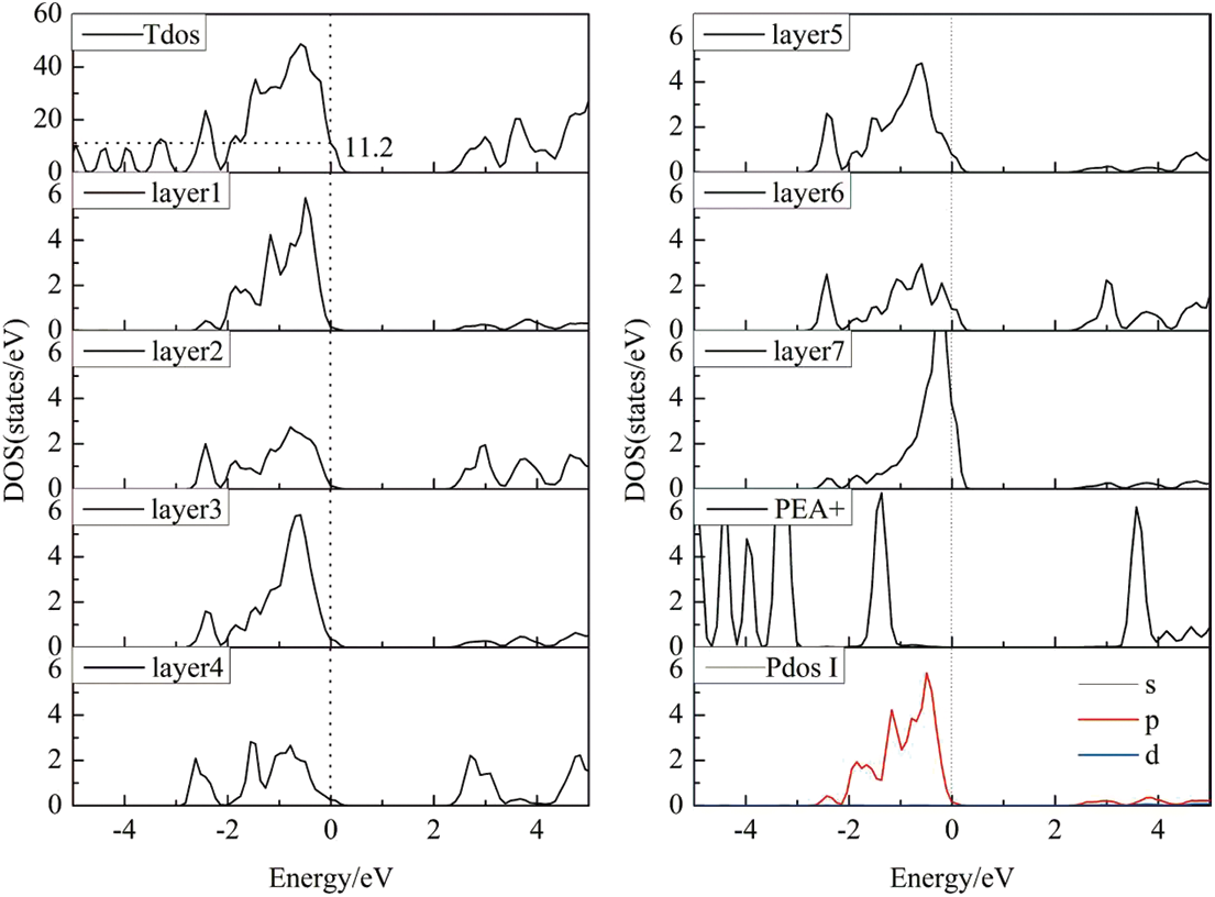
Figure 4: Density of states of the PEA+-CsPbI3 (110) passivation system
The Bader atomic charges [34] and Charge density difference of the PEA+-CsPbI3 system after passivation were calculated to analyze the scale of surface electron transfer. The Charge density difference after passivation can be calculated using formula (2).
In formula (2), ρPEA/CsPbI3 is the total charge density of the PEA+-CsPbI3 (110) system.
Fig. 5 shows the charge density difference of the PEA+-CsPbI3 passivation system. Fig. 5a is the overall charge density difference map of the passivation system, which clearly shows the schematic of charge transfer. Fig. 5b is a partial enlarged diagram of charge density difference. Yellow areas mean gaining electrons, and light green areas mean losing electrons. The charge of the adsorption surface is redistributed, C and N atoms lose electrons (light green areas), while I atom gets electrons (yellow areas). A large number of electron clouds overlap, which indicating that the PEA+-CsPbI3 system has a strong bonding effect at the adsorption site. The electron concentration is the highest at the adsorption site, and the further away from the adsorption site, the lower the electron concentration.
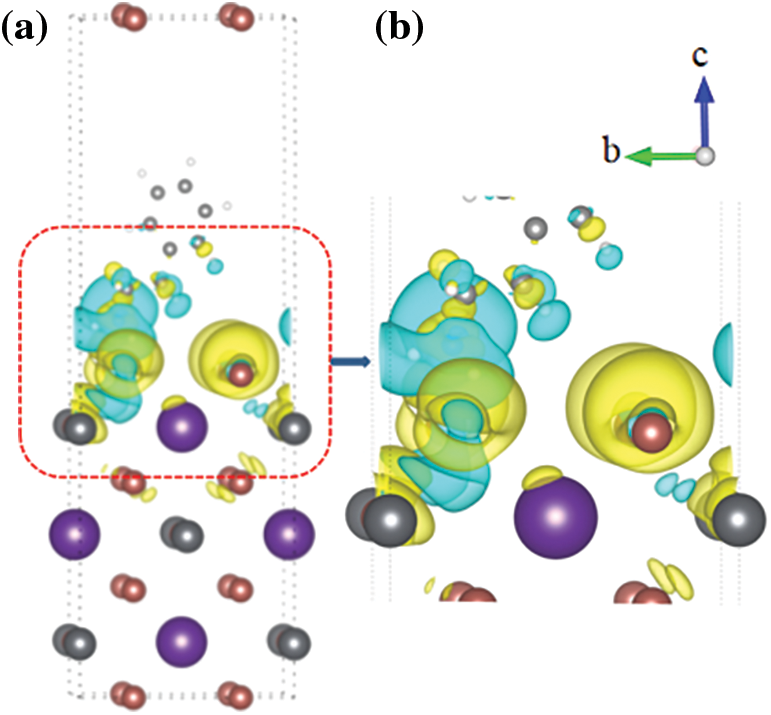
Figure 5: The charge density difference of the PEA+-CsPbI3 adsorption system ((a) is the overall side view, (b) is a partial enlarged view)
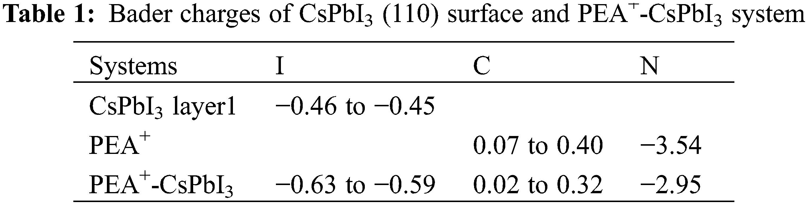
The simple and intuitive schematic figure of charge density difference cannot accurately analyze the specific charge transfer amount at the adsorption site. Therefore, we calculated the Bader charges of the clean CsPbI3 (110), PEA+ and the adsorption system PEA+-CsPbI3, respectively. The surface states of CsPbI3 (110) chiefly originate from the contribution of I, N, and C atoms of non-benzene ring groups with PEA+ make a greater contribution to eliminating surface states. Therefore, only Bader charges of the I atoms of clean CsPbI3 (110), and those of the N and C atoms of non-benzene ring groups with PEA+, and those of I, N and C atoms in the corresponding adsorption system PEA+-CsPbI3 are given in Table 1. These I atoms’ Bader charges on the first layer of clean CsPbI3 (110) are in the range of −0.46 to −0.45 e, and the Bader charges of N and C atoms on the adsorbed material PEA+ are 0.07 to 0.40 and −3.54 e, respectively. It can also be seen from the Table 1 that the Bader charge values of I, N and C atoms on the PEA+-CsPbI3 system, the Bader charges of the corresponding I atoms are in the range of −0.63 to −0.59 e, and those of N and C are 0.02 to 0.32 and −2.95 e, respectively. According to the value of the Bader charge, it is found that the I atoms of CsPbI3 form bonds with the N and C atoms of the adsorbent PEA+, respectively, and the I atoms can obtain electrons from the N and C atoms bonded to it, thereby reducing the CsPbI3 (110) surface states.
This paper uses the first principles calculation of density functional theory to study electronic properties of CsPbI3 (110) surface. Based on this, the surface states with the CsPbI3 (110) surface near the Fermi level are passivated by PEA+ molecule. The micro mechanism is deeply discussed by investigating the stability and electronic structure of the passivation system. The calculated results of adsorption energy show that the model with I atom at the end faces to combine with PEA+ molecule is stable. The results of surface electronic structure calculation reveal that surface states on the CsPbI3 (110) surface near the Fermi level are mainly contributed by I-5p orbital. Its value of DOS is 18.3 (relative value) on the unpassivated CsPbI3 (110) surface near the Fermi level. Electronic structure of the PEA+-CsPbI3 system calculations demonstrates that the value of DOS has reduced from 18.3 to 11.2, and the passivation rate is 38.8%. The material PEA+ can improve surface states on the CsPbI3 (110) surface, and it is a potential passivation material. Bader charge analysis shows that electrons are transferred from passivation material to perovskite, which reduces the hole concentration in perovskite. Considering the experimental application of PEA+, our theoretical study is expected to inspire the experimental study of PEA+ in perovskite materials, leading to the development of high-performance perovskite solar cells.
Acknowledgement: The authors would like to thank the Gansu Supercomputer Center and School of Chemical Engineering, Northwest University.
Funding Statement: The authors acknowledge the support from the National Natural Science Foundation of China (11764027), the GH Fund B (202202022563), Youth Fund Project of Lanzhou City College (LZCU-QN2021-08), Gansu Provincial Key Talent Projects in 2020, Gansu Province Colleges and Universities Industry Support Project (2020C-30), and Provincial Key Talent Project in 2020 (Mechanical Equipment Green Reconstruction Surface Engineering Innovation Talent Team Construction Project).
Conflicts of Interest: The authors declare that they have no conflicts of interest to report regarding the present study.
References
1. Ran, C. X., Xu, J. T., Gao, W. Y., Huang, C. M., Dou, S. X. (2018). Defects in metal triiodide perovskite materials towards high-performance solar cells: Origin, impact, characterization, and engineering. Chemical Society Reviews, 47(12), 4581–4610. DOI 10.1039/C7CS00868F. [Google Scholar] [CrossRef]
2. Ono, L. K., Liu, S. Z., Qi, Y. (2020). Reducing detrimental defects for high-performance metal halide perovskite solar cells. Angewandte Chemie International Edition, 59(17), 6676–6698. DOI 10.1002/anie.201905521. [Google Scholar] [CrossRef]
3. Landi, G., Neitzert, H. C., Barone, C., Mauro, C., Lang, F. L. et al. (2017). Correlation between electronic defect states distribution and device performance of perovskite solar cells. Advanced Science, 4(10), 1700183.1–1700183.11. DOI 10.1002/advs.201700183. [Google Scholar] [CrossRef]
4. Shao, Y. C., Yuan, Y. B., Huang, J. S. (2016). Correlation of energy disorder and open-circuit voltage in hybrid perovskite solar cells. Nature Energy, 1(1), 15001.1–15001.6. DOI 10.1038/nenergy.2015.1. [Google Scholar] [CrossRef]
5. Zu, F. S., Amsalem, P., Ralaiarisoa, M., Schultz, T., Schlesinger, R. et al. (2017). Surface state density determines the energy level alignment at hybrid perovskite/electron acceptors interface. ACS Applied Materials & Interface, 9, 41546–41552. DOI 10.1021/acsami.7b12586. [Google Scholar] [CrossRef]
6. Zhu, L. F., Xu, Y. Z., Zhang, P. P., Shi, J. J., Zhao, Y. H. et al. (2017). Investigation on the role of lewis bases in the ripening process of perovskite films for highly efficient perovskite solar cells. Journal of Materials Chemistry A, 5, 20874–20881. DOI 10.1039/C7TA05378A. [Google Scholar] [CrossRef]
7. Fu, S., Li, X. D., Wan, L., Wu, Y. L., Zhang, W. X. et al. (2019). Efficient passivation with lead pyridine-2-carboxylic for high-performance and stable perovskite solar cells. Advanced Energy Materials, 9(35), 1901852.1–1901852.10. DOI 10.1002/aenm.201901852. [Google Scholar] [CrossRef]
8. Yang, Z., Dou, J. J., Kou, S., Dang, J. L., Ji, Y. Q. et al. (2020). Multifunctional phosphorus-containing lewis acid and base passivation enabling efficient and moisture-stable perovskite solar cells. Advanced Functional Materials, 30(15), 1910710.1–1910710.9. DOI 10.1002/adfm.201910710. [Google Scholar] [CrossRef]
9. Zhao, X. M., Yao, C., Liu, T. R., Hamill, J. C., Ndjawa, G. O. N. et al. (2019). Extending the photovoltaic response of perovskite solar cells into the near-infrared with a narrow-bandgap organic semiconductor. Advanced Materials, 31(49), 1904494.1–1904494.9. DOI 10.1002/adma.201904494. [Google Scholar] [CrossRef]
10. Li, M., Yang, Y. G., Wang, Z. K., Kang, T., Wang, Q. et al. (2019). Perovskite grains embraced in a soft fullerene network make highly efficient flexible solar cells with superior mechanical stability. Advanced Materials, 31(25), 1901519.1–1901519.8. DOI 10.1002/adma.201901519. [Google Scholar] [CrossRef]
11. Patil, J. V., Mali, S. S., Hong, C. K. (2019). A thiourea additive-based quadruple cation lead halide perovskite with an ultra-large grain size for efficient perovskite solar cells. Nanoscale, 11(45), 21824–21833. DOI 10.1039/C9NR07377A. [Google Scholar] [CrossRef]
12. Zhou, W., Li, D., Xiao, Z. G., Wen, Z. L., Zhang, M. M. et al. (2019). Zwitterion coordination induced highly orientational order of CH3NH3PbI3 perovskite film delivers a high open circuit voltage exceeding 1.2 V. Advanced Functional Materials, 29(23), 1901026.1–1901026.11. DOI 10.1002/adfm.201901026. [Google Scholar] [CrossRef]
13. Guo, G. C., Wang, C. H., Luo, S. W., Ming, B. M., Wang, B. R. et al. (2020). First-principles study of C3N nanoribbons as anode materials for Li-ion batteries. Physics Letters A, 384(28), 126741.1–126741.7. DOI 10.1016/j.physleta.2020.126741. [Google Scholar] [CrossRef]
14. Halwidl, D., Stöger, B., Mayr-Schmölzer, W., Pavelec, J., Fobes, D. et al. (2016). Adsorption of water at the SrO surface of ruthenates. Nature Materials, 15(4), 450–455. DOI 10.1038/NMAT4512. [Google Scholar] [CrossRef]
15. Zhu, H. W., Liu, Y. H., Eickemeyer, F. T., Pan, L. F., Ren, D. et al. (2020). Tailored amphiphilic molecular mitigators for stable perovskite solar cells with 23.5% efficiency. Advanced Materials, 32(12), 1907757.1–1907757.8. DOI 10.1002/adma.201907757. [Google Scholar] [CrossRef]
16. Guo, P. F., Ye, Q., Yang, X. K., Zhang, J., Xu, F. et al. (2019). Surface & grain boundary co-passivation by fluorocarbon based bifunctional molecules for perovskite solar cells with efficiency over 21%. Journal of Materials Chemistry A, 7(6), 2497–2506. DOI 10.1039/C8TA11524A. [Google Scholar] [CrossRef]
17. Huang, X., Guo, H., Wang, K., Liu, X. B. (2017). Ionic liquid induced surface trap-state passivation for efficient perovskite hybrid solar cells. Organic Electronics, 41, 42–48. DOI 10.1016/j.orgel.2016.11.031. [Google Scholar] [CrossRef]
18. Zhang, H., Wu, Y. Z., Shen, C., Li, E. P., Yan, C. X. et al. (2019). Efficient and stable chemical passivation on perovskite surface via bidentate anchoring. Advanced Energy Materials, 9(13), 1803573.1–1803573.9. DOI 10.1002/aenm.201803573. [Google Scholar] [CrossRef]
19. Zhao, S. H., Xie, J. S., Cheng, G. H., Xiang, Y. R., Zhu, H. Y. et al. (2018). General nondestructive passivation by 4-fluoroaniline for perovskite solar cells with improved performance and stability. Small, 14(50), 1803350.1–1803350.11. DOI 10.1002/smll.201803350. [Google Scholar] [CrossRef]
20. Zheng, X. P., Chen, B., Dai, J., Fang, Y. J., Bai, Y. et al. (2017). Defect passivation in hybrid perovskite solar cells using quaternary ammonium halide anions and cations. Nature Energy, 2(7), 1–9. DOI 10.1038/nenergy.2017.102. [Google Scholar] [CrossRef]
21. Du, X. Z., Qiu, R. Z., Zou, T. Y., Chen, X. X., Chen, H. J. (2019). Enhanced uniformity and stability of Pb-Sn perovskite solar cells via Me4NBr passivation. Advanced Materials Interfaces, 6(14), 1900413. DOI 10.1002/admi.201900413. [Google Scholar] [CrossRef]
22. Moriya, Y., Ishikawa, R., Akiyama, S., Ueno, K., Shirai, H. et al. (2019). Self-assembled fluorinated polymer passivation layer for efficient perovskite thin-film solar cells. Chemistry Letters, 49(1), 87–90. DOI 10.1246/cl.190692. [Google Scholar] [CrossRef]
23. Bi, D. Q., Yi, C. Y., Luo, J. S., Décoppet, J. D., Zhang, F. et al. (2016). Polymer-templated nucleation and crystal growth of perovskite films for solar cells with efficiency greater than 21%. Nature Energy, 1(10), 16142.1–16142.5. DOI 10.1038/nenergy.2016.142. [Google Scholar] [CrossRef]
24. Yang, S. W., Park, B. W., Jung, E. H., Jeon, N. J., Kim, Y. C. et al. (2017). Iodide management in formamidinium-lead-halide-based perovskite layers for efficient solar cells. Science, 356(6345), 1376–1379. DOI 10.1126/science.aan2301. [Google Scholar] [CrossRef]
25. Jiang, Q. J., Zhao, Y., Zhang, X. W., Yang, X. L., Chen, Y. et al. (2019). Surface passivation of perovskite film for efficient solar cells. Nature Photonics, 13(7), 460–466. DOI 10.1038/s41566-019-0462-y. [Google Scholar] [CrossRef]
26. Wang, Y., Zhang, T. Y., Kan, M., Li, Y. H., Wang, T. et al. (2018). Efficient α-CsPbI3 photovoltaics with surface terminated organic cations. Joule, 2(10), 2065–2075. DOI 10.1016/j.joule.2018.06.013. [Google Scholar] [CrossRef]
27. Kresse, G., Furthmüller, J. (1996). Efficiency of ab-initio total energy calculations for metals and semiconductors using a plane-wave basis set. Computational Materials Science, 6(1), 15–50. DOI 10.1016/0927-0256(96)00008-0. [Google Scholar] [CrossRef]
28. Kresse, G., Furthmüller, J. (1996). Efficient iterative schemes for ab initio total-energy calculations using a plane-wave basis set. Physical Review B, 54, 11169–11186. DOI 10.1103/PhysRevB.54.11169. [Google Scholar] [CrossRef]
29. Perdew, J. P., Burke, K., Ernzerhof, M. (1998). Generalized gradient approximation made simple. Physical Review Letters, 77(18), 3865–3868. DOI 10.1103/PhysRevLett.77.3865. [Google Scholar] [CrossRef]
30. Kresse, G., Joubert, D. (1999). From ultrasoft pseudopotentials to the projector augmented-wave method. Physical Review B, 59(3), 1758–1775. DOI 10.1103/PhysRevB.59.1758. [Google Scholar] [CrossRef]
31. Zhou, J. G., Causon, D. M., Mingham, C. G., Ingram, D. M. (2001). The surface gradient method for the treatment of source terms in the shallow-water equations. Journal of Computational Physics, 168(1), 1–25. DOI 10.1006/jcph.2000.6670. [Google Scholar] [CrossRef]
32. Blöchl, P. E., Jepsen, O., Andersen, O. K. (1994). Improved tetrahedron method for brillouin-zone integrations. Physical Review B, 49(23), 16223–16244. DOI 10.1103/PhysRevB.49.16223. [Google Scholar] [CrossRef]
33. Bao, L. K., Kong, Z. Z., Qu, D. Y., Duan, Y. H. (2021). First-principles investigation on the structures, energies and electronic properties of low-index surfaces of mg2pb. Materials Chemistry and Physics, 260, 124028.1–124028.8. DOI 10.1016/j.matchemphys.2020.124028. [Google Scholar] [CrossRef]
34. Bader, F. R. (1990). Atoms in molecule: A quantum theory, New York: Oxford University Press. DOI 10.1002/bbpc.19910951039. [Google Scholar] [CrossRef]
Cite This Article
 Copyright © 2023 The Author(s). Published by Tech Science Press.
This work is licensed under a Creative Commons Attribution 4.0 International License , which permits unrestricted use, distribution, and reproduction in any medium, provided the original work is properly cited.
 Downloads
 Citation Tools