
 Submit a Paper
 Propose a Special lssue
 Open Access
ARTICLE
High Linear Voltage Gain in QZNC Through Synchronizing Switching Circuits
1 Department of EEE, REC Lab, SSN College of Engineering, Chennai, 603110, Tamil Nadu, India
2 Department of ECE, SSN College of Engineering, Chennai, 603110, Tamil Nadu, India
* Corresponding Author: S. Harika. Email:
Intelligent Automation & Soft Computing 2023, 36(1), 895-910. https://doi.org/10.32604/iasc.2023.031829
Received 27 April 2022; Accepted 29 June 2022; Issue published 29 September 2022
 View Full Text
 Download PDF
Abstract
The solar powered systems require high step-up converter for efficient energy transfer. For this, quasi-impedance network converter has been introduced. The quasi-impedance network converter (QZNC) is of two types: type-1 and type-2 configuration. Both the type-1 and type-2 QZNC configurations have drooping voltage gain profile due to presence of high switching noise. To overcome this, a new quasi-impedance network converter synchronizing the switching circuit with low frequency noise has been proposed. In this paper, the proposed QZNC configuration utilizes the current controlling diode to prevent the output voltage drop. Thus, the suggested topology provides linear high voltage gain profile, low load voltage ripple, and reduced impedance network stress and device stress. Therefore, the efficiency of proposed QZNC has been improved. The topology description, working principle, parameter design and comparison with traditional converters are illustrated. And finally, both simulation and practical results are presented to confirm the converter characteristics and performance. From the results, it has been found that the performance of the suggested topology is better as it achieves a higher efficiency of 81% and hence, it is suitable for high power applications.Keywords
The renewable energy resources such as solar and wind energy are appeared as an alternate energy resource in many industrial applications. Since the industrial sectors faces the problem of shortage of conventional fossil fuel. Therefore, the alternate energy chosen should available abundantly and eco-friendly [1]. In view of this, among the renewable energy resources, the solar energy is mostly preferred as it meets the demand efficiently. Whereas the output from such solar energy resources is low, and far from the high voltage dc link. So, the demand for high step-up dc-dc converter is risen and more research on these topologies has been carried out. Most of the industrial applications such as electric vehicle power supplies, Light Emitting Diode (LED) lighting, X-ray systems, electric vehicle charging system, and grid connected systems requires high boost ratio dc-dc converters [2].
The most commercially used topology for solar energy is the boost Direct Current (DC-DC) converter [3] which achieves higher gain at high duty ratio. Due to this, the device losses increase which results in the degradation of the converter efficiency [4]. Moreover, considering the effect of parasitic elements, the duty ratio of the traditional boost converter is limited [5]. In addition to that, many topologies such as cascading two boost converters [6], coupled inductors [7] and interleaving concept [8], converter with switched capacitor [9], converter with switched inductor [10], voltage lift technique [11] have been presented. However, the size of the converter is increased making it more complex [12], and it needs to be worked at high duty ratio [13]. To overcome this, Z-source converter has been proposed in the year 2002 [14]. Whereas it has the drawback of the discontinuous source current which affects the converter performance [15]. Thus, the QZNC has gained more attraction in the power electronics sector due to its unique feature of high voltage gain at low duty ratio [16], the continuous source current [17] and higher efficiency [18]. It works in both buck and boost operation based on the load profile [19]. These types of converters are applied in photovoltaic system [20], electric vehicle charging station [21] and distributed generation [22]. This converter uses the impedance network placed between the source and load to boost the voltage. The boost factor depends on the shoot-through duty ratio. By incorporating the impedance-network configuration, the requirement of passive components is lowered. The impedance network is in X-shape with interconnection of inductors and capacitors [23].
QZNC is of two types: type-1 [24] and type-2 configuration [25]. The output inductor in the type-1 configuration has been replaced with the diode in the type-2 QZNC, hence, the voltage gain has increased [26]. But the type-2 QZNC has limited duty ratio (D < 0.33) [27] and has the problem of heavy voltage stress across the network, thereby the converter behavior is affected. The reason for limited duty ratio for operating the converter is due to high switching noise. In DC-DC converter, dead time exists in between turning ON and OFF of the power switch. During dead time, reverse current flows through the circuit which degrades the converter performance. To commutate this, capacitor draws high starting current from the power supply. Due to this, whenever the input voltage to output voltage ratio increases, the capacitor draws higher starting current, thereby, the output voltage drops. This results in the converter voltage gain profile to droop after certain value of duty ratio. Also, the voltage ringing occurs in the converter circuit if the negative current is not commutated properly. As the capacitor takes more time to commutate the reverse current, the high switching noise exists. Because of high switching noise and ESR present in the switching capacitor limits the converter efficiency for wide range of input voltage to output voltage ratio. Since the existing QZNC comprises of capacitors in the network, the duty ratio of the converter is limited and the voltage stress across the network as well as across the power device increases. This result in the existing type-1 and type-2 QZNC is not preferred for high power applications.
In this paper, a new type of QZNC has been proposed with low switching noise. The low switching noise is obtained using current controlling diode. But the diode should have short reverse recovery time. Because, the diode with long reverse recovery time takes more time to commutate the negative current and also, the parasitic inductance present in it increases the dIF/dt. Due to increased dIF/dt, the voltage stress across the network increases. Thus, the fast reverse recovery diode FR107 has been used in the proposed topology, thereby, low switching noise operation is obtained. This extends the new QZNC operation for wide range of input voltage to output voltage ratio and achieves high voltage gain compared to other topologies. Also, the voltage stress across the impedance network as well as across the power device is reduced. The reduced output voltage ripple is obtained with the proper designing of converter parasitic elements. This results in the improved converter efficiency for wide range of duty cycle. Hence, the proposed QZNC can be used for high power application. To confirm the performance, the comparative analysis has been carried out between the new modified QZNC topology with the conventional boost, ZNC and type-1 and type-2 QZNC configurations. The parameters accounted for the analysis are voltage gain, load voltage ripple, capacitor voltage stress, diode voltage stress, device voltage stress and efficiency. The performance of the parameters has been computed for different duty ratio and compared.
The organization of the paper is as follows: The operating principle and design guideline of the proposed topology have been discussed in Section 2 and Section 3. Section 4 illustrates the simulation results and comparative analysis of the three converter topologies. Section 5 deals with the hardware results of the proposed converter. Section 6 concludes the paper.
2 Operating Principle of Proposed QZNC
The concept of QZNC attracted the power electronics engineers because of its unique feature illustrated in [28] which is imperative for the DC-DC converter. The impedance-network (LDC unit) is placed between the supply (in cascading with the supply) and load [29]. The pictorial representation of the type-1 QZNC is shown in Fig. 1. Due to the presence of output inductor (Lo), the type-1 converter performance is limited to the D < 0.37 which limits converter gain. Thus, the output inductor is replaced by diode (Do) in type-2 QZNC as shown in Fig. 2. Though, high voltage gain is achieved, the duty ratio is still limited to D < 0.33 and the converter undergoes high stress across the device as well as the impedance network. To overcome these demerits, a new type of QZNC has been proposed, and it is depicted in Fig. 3. The proposed converter behaves better for the ranges of duty cycle (D) upto 0.49. In this section, the working principle and modes of operation of the proposed converter is explained.
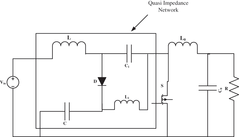
Figure 1: Type-1 QZNC
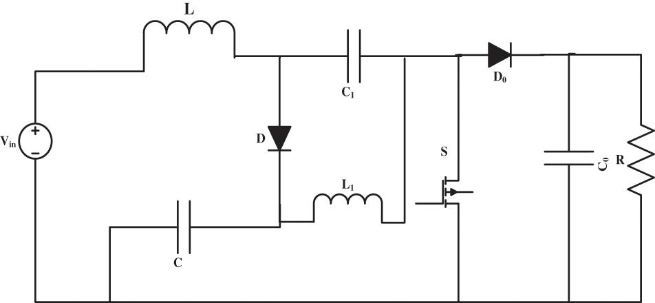
Figure 2: Type-2 QZNC
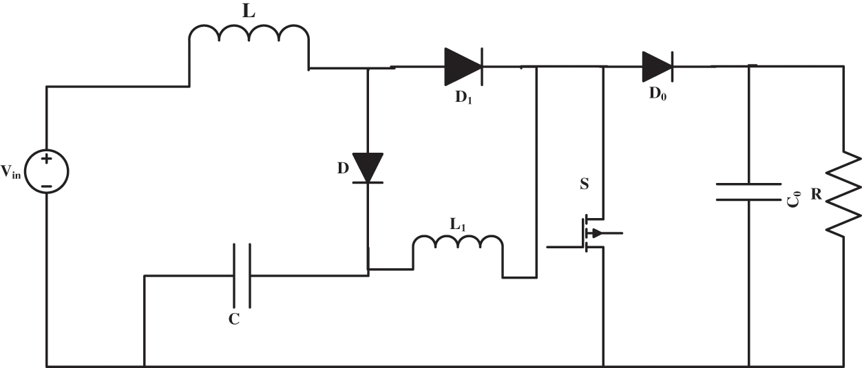
Figure 3: Proposed QZNC
The inductors L, L1, capacitor C, and diode D, D1 constitute the impedance network. The operation of the proposed converter is described in two modes as presented in Figs. 4a and 4b, and it is explained below.
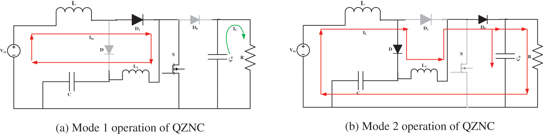
Figure 4: (a) Mode 1 operation of QZNC (b) Mode 2 operation of QZNC
Mode 1 [0 ∼ t0]: When switch S and diode D1 are in conduction, the pre-charged capacitor discharges the current through the inductors (L1 and L2), thus, reverse biases the diode D and D0. Due to this, the current through the inductor increases linearly as shown in Fig. 5. Once the inductor current reaches the steady state value, the inductor starts to discharge ending mode-1 operation.
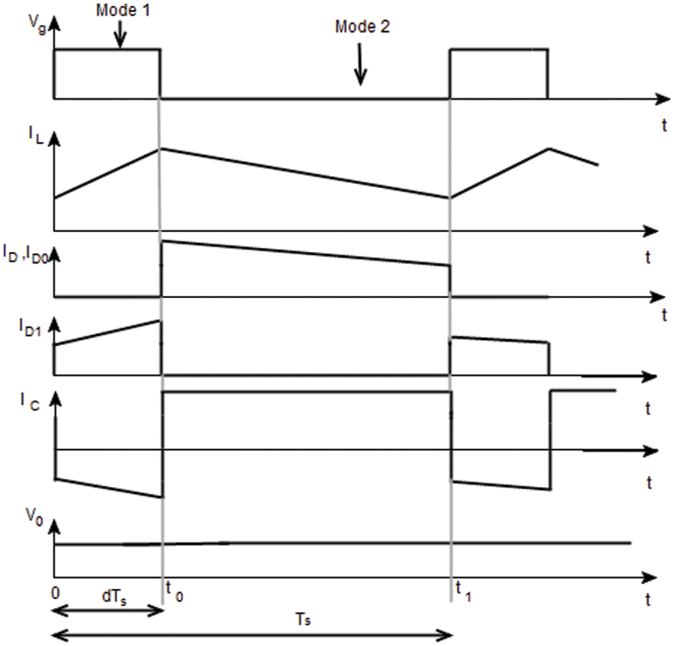
Figure 5: Waveforms of the proposed QZNC
Mode 2 [t0 ∼ t1]: When switch S is in off state, the capacitor C is charged by the inductors (L1 and L2). This turns on the diode D and D0, whereas the diode D1 is in off condition. Now, the current through the inductor decreases linearly as shown in Fig. 5. The load is powered by impedance network.
The QZNC emerges as an eye-catching topology due to its superior performance such as low output voltage ripple and reduced stress across power device. These features are attained by proper designing of the converter. Thus, the equations derived for the passive elements describe in this section. The voltage relationship of the new topology is obtained by using the voltage-second balance for the inductor [30] as in Eq. (1).
According to mode2, the load voltage of the converter is as in Eq. (2)
By manipulating Eqs. (1) and (2), the gain of the converter is as in Eq. (3)
Assuming loss free converter, the current through inductor is found using the Eq. (4).
Then, the inductor expression is as in Eq. (5),
where,
d = duty ratio
The voltage ripple of the capacitor is expressed as the function of inductor current as it is equal to the capacitor current during mode 1. From this, the capacitor is found by the expression and stated as in Eq. (6),
where,
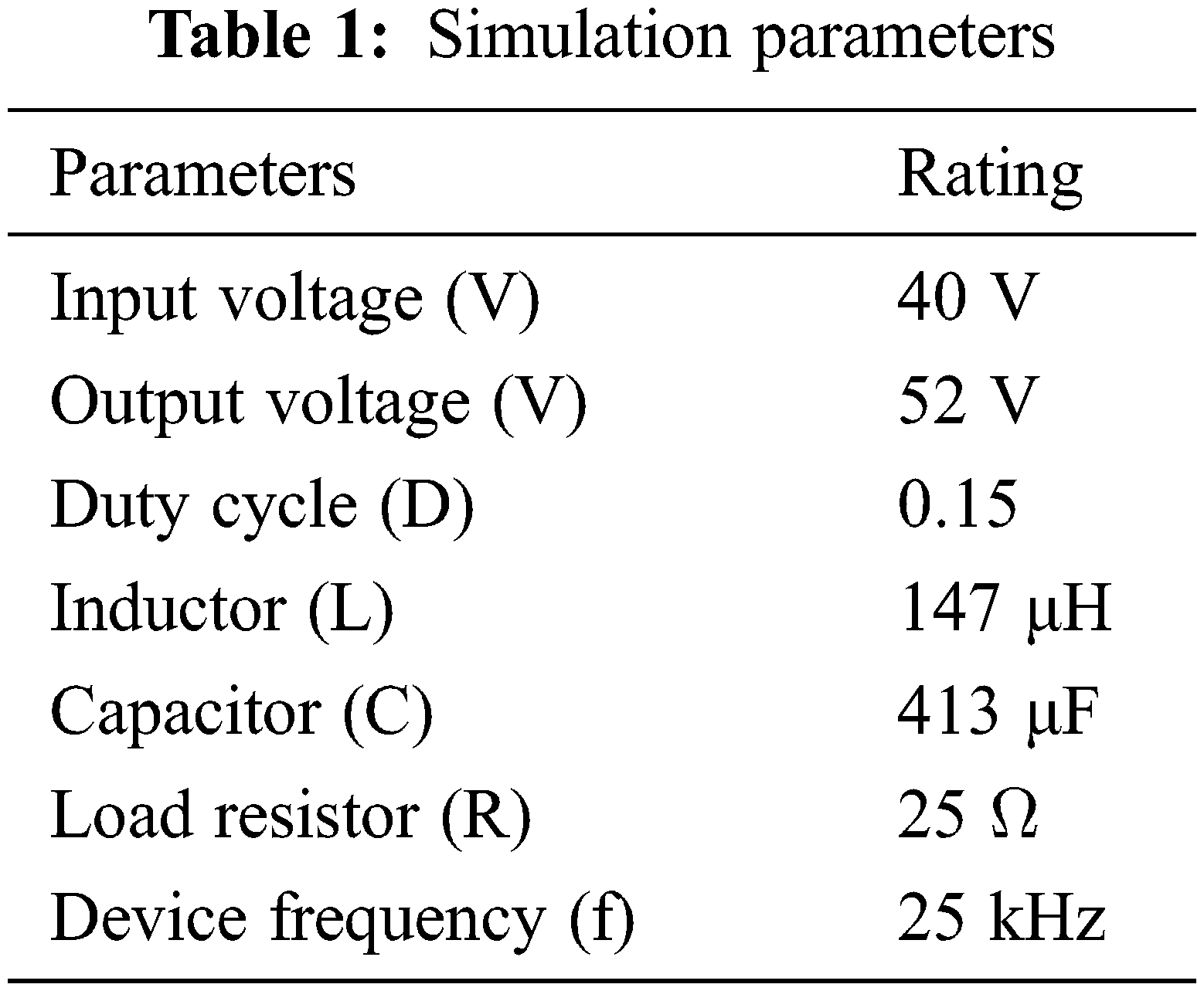
The problems associated with the existing topologies for high step-up voltage applications have been overcome by the proposed QZNC. The modifications performed in the proposed topology, and it is operations are clearly presented in the Section 2. Also, distinctive features are achieved by proper design which has been described in Section 3. Based on the Eqs. (1)–(6), the proposed converter has been designed and simulated in MATLAB/SIMULINK. The simulations parameters are listed in Tab. 1 are identical for all the three converters. The simulation results are studies and compared with other topologies in terms of its performance. The parameters accounted for analysis are voltage gain, load voltage ripple, capacitor voltage stress, diode voltage stress, device voltage stress and efficiency [31]. The parameters are computed for different duty ratios [32].
The main feature of the proposed QZNC is linearly higher voltage gain characteristics. The voltage gain characteristics of all the three QZNC for distinct values of duty ratio has been depicted in Fig. 6. From Fig. 6, it is clear that the suggested topology has increasing gain characteristics, whereas the other topologies has drooping characteristics due to its operation at limited duty ratio.

Figure 6: Voltage gain vs. duty ratio
As depicted in Fig. 6, the voltage gain of the type-2 converter starts to decrease when the duty ratio is increased beyond 0.33 even though it has high voltage gain than the proposed converter. Also, the type-1 converter starts to droop when the D > 0.37. This clearly shows that the existing topology works upto the duty ratio of 0.37 only. In contrast, the recommended converter performs well for D ≤ 0.49.
Another main feature of the proposed QZNC is reduced load voltage ripple. The behavior of load voltage ripple characteristics of all the three QZNC for different duty ratio has been studied and its pictorial representation is depicted in Fig. 7. Though type-1 configuration has lower load voltage ripple, it has the drawback of low voltage gain than the proposed and type-2 topologies. Thus, from the Fig. 7, it has been inferred that the proposed topology is preferred as it has low load voltage ripple compared to type-2 topology.

Figure 7: Load voltage ripple vs. duty ratio
As discussed earlier, the proposed QZNC achieves high step-up output voltage at low duty ratio. Owing to this, the voltage spike across the power device, diode and capacitor has been reduced drastically. To ensure this, the voltage stress across the switch, diode, and capacitor for different duty ratios of all the three converters has been computed and compared with each other. The voltage stress characteristics have been depicted in Figs. 8 to 9. The comparison of network diode voltage stress for various values of voltage gain is presented in Fig. 8. From 8, it could be inferred that the proposed QZNC has reduced voltage stress across the diode compared with type-1 and type-2 QZNC.

Figure 8: Diode voltage stress

Figure 9: (a) Voltage stress across the switch
Fig. 9a shows the voltage stress across the device for all the three converters. It is implied that the proposed QZNC has lower voltage stress across the device compared with the existing configuration. Furthermore, it is inferred that for D > 0.1, there is a drastic reduction in voltage stress across the device for the proposed QZNC against the other topologies. Also, the recommended proposed QZNC has lower capacitor voltage stress compared with type-1 and type-2 QZNC as shown in Fig. 9b. From Fig. 9b, it is implied that compared with other topologies, the suggested converter has drastic reduction in the voltage stress across the device for D > 0.1.
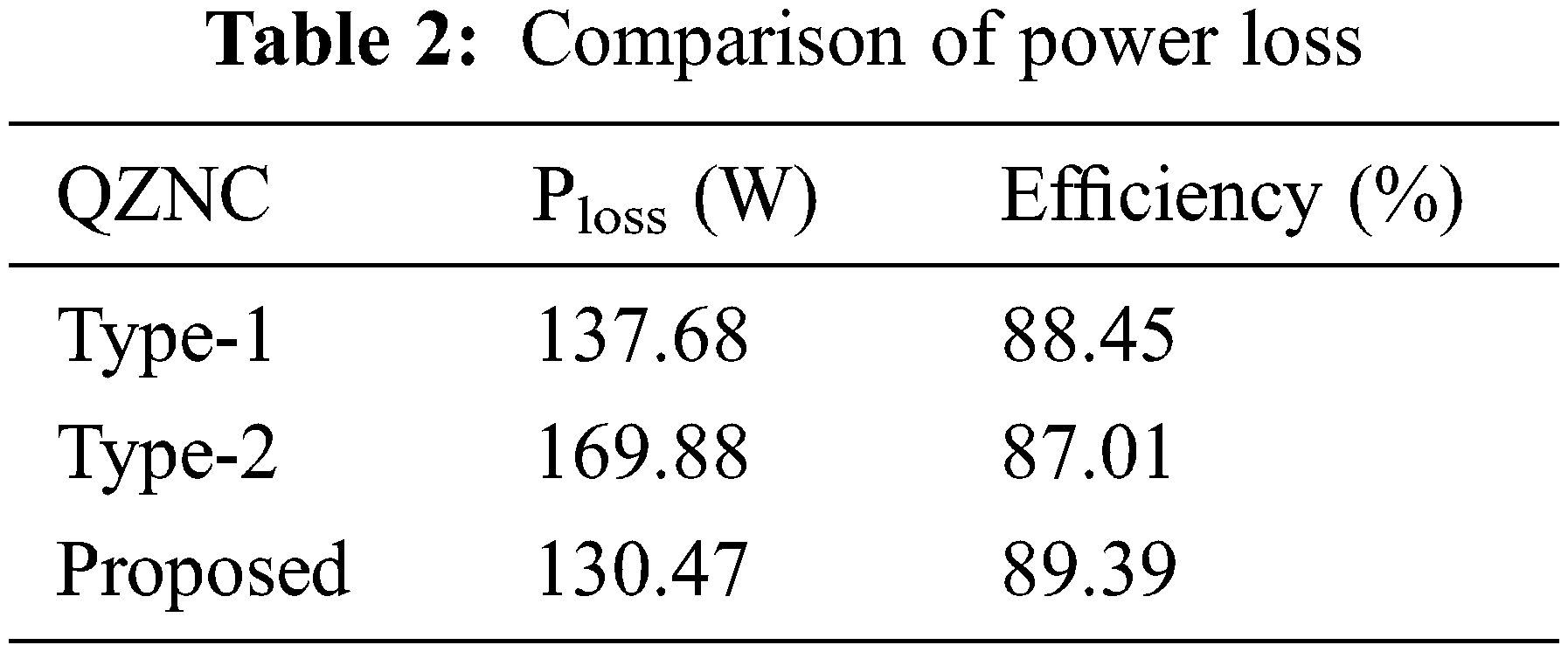
The efficiency of all the three QZNC are evaluated and compared with each other. The power loss (Ploss) computation for all the three topologies for the specified duty ratio (D = 0.15) is presented in Tab. 2. The loss calculation is shown below [33].
The device loss is,
The diode loss is as in Eq. (8)
The inductor loss is as in Eq. (9)
The Capacitor loss is as in Eq. (10)
where,
Hence, the efficiency of QZNC is improved against the suggested network. The efficiency comparison for different duty ratio is depicted in Fig. 10. From Fig. 10, it could be seen that the recommended QZNC has high efficiency for all the values of duty ratio compared with the existing topologies.
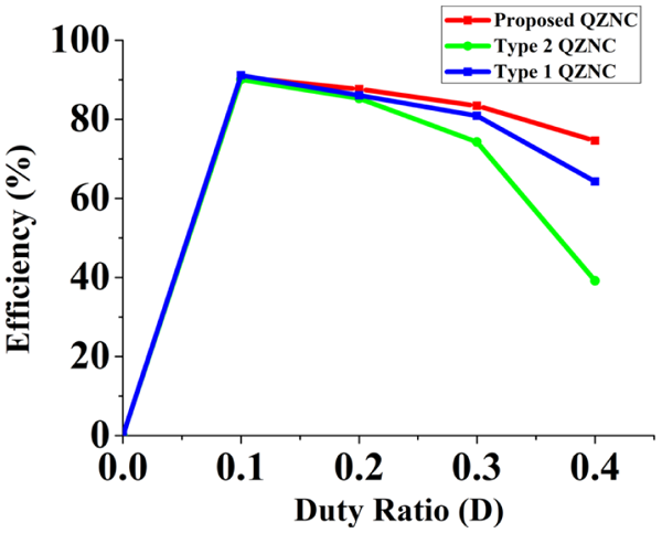
Figure 10: Efficiency vs. duty ratio
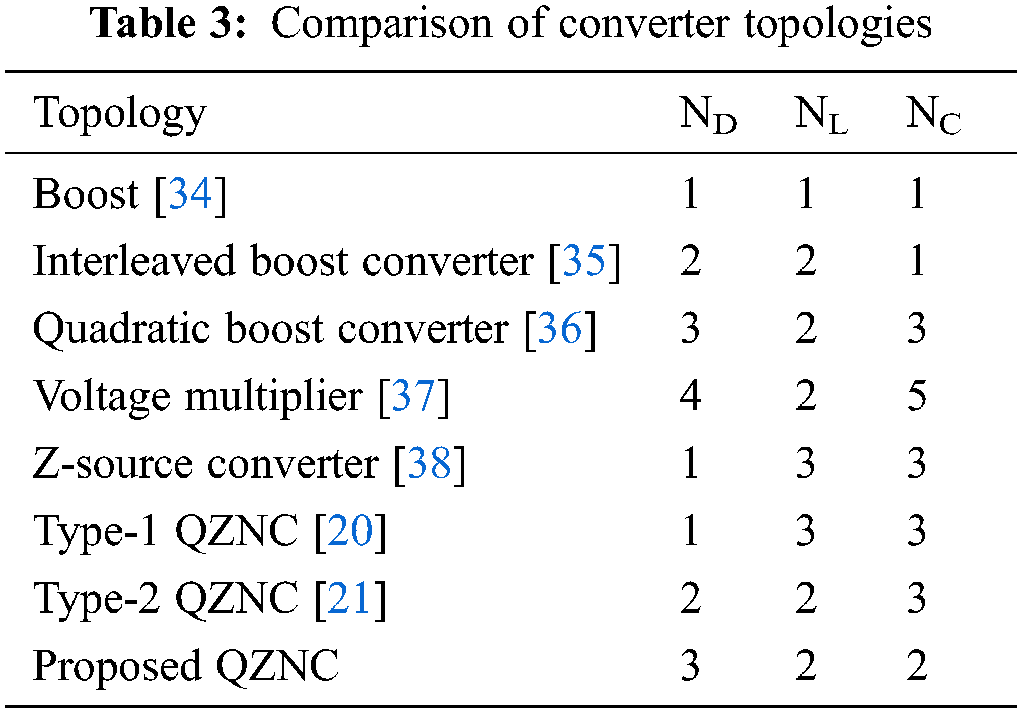
The comparison of proposed topology with other converter topologies for the specified duty ratio (D = 0.15) in terms of converter components are listed in Tab. 3. The number of diodes, inductors and capacitors are denoted as ND, NL and NC.
The simulation waveform of proposed topology is presented in this section. The supply and load waveforms of new QZNC shown in Fig. 11. The stress across the device shown in Fig. 12.
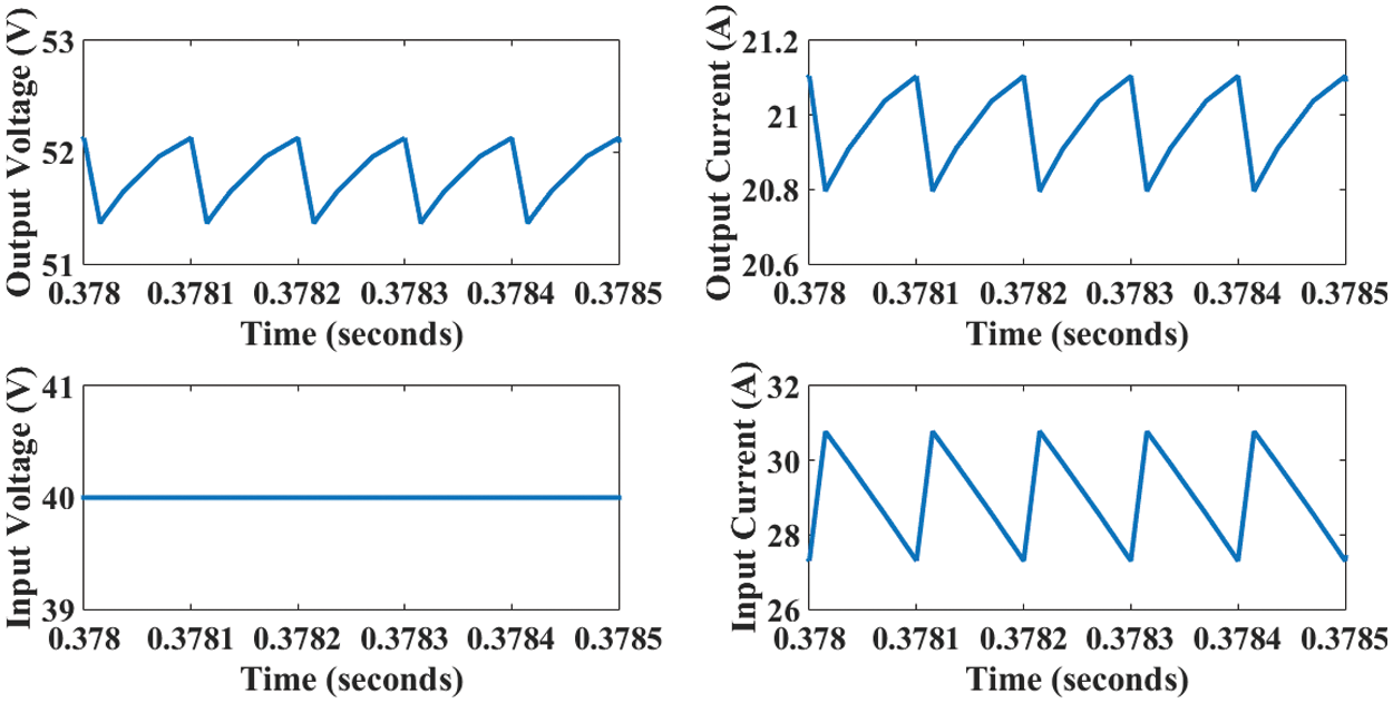
Figure 11: Supply and load voltage of proposed QZNC
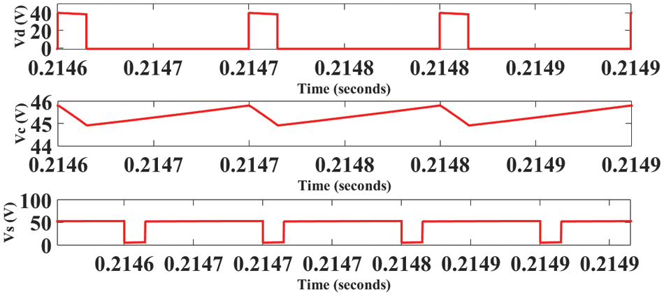
Figure 12: Stress waveform of proposed QZNC
The supply voltage of 40 V stepped to 52.12 V for D = 0.15 as shown in Fig. 11. Thus, the converter voltage gain is 1.303 based on Eq. (3). From Fig. 11, it is observed that the ripple of the load voltage is less which is 0.01 V. The pictorial representation of the voltage across the network diode (Vd), network capacitor (Vc) and across the device (Vs) is depicted in Fig. 12.
For the suggested QZNC, the voltage stress across the network diode (Vds) is 0.99
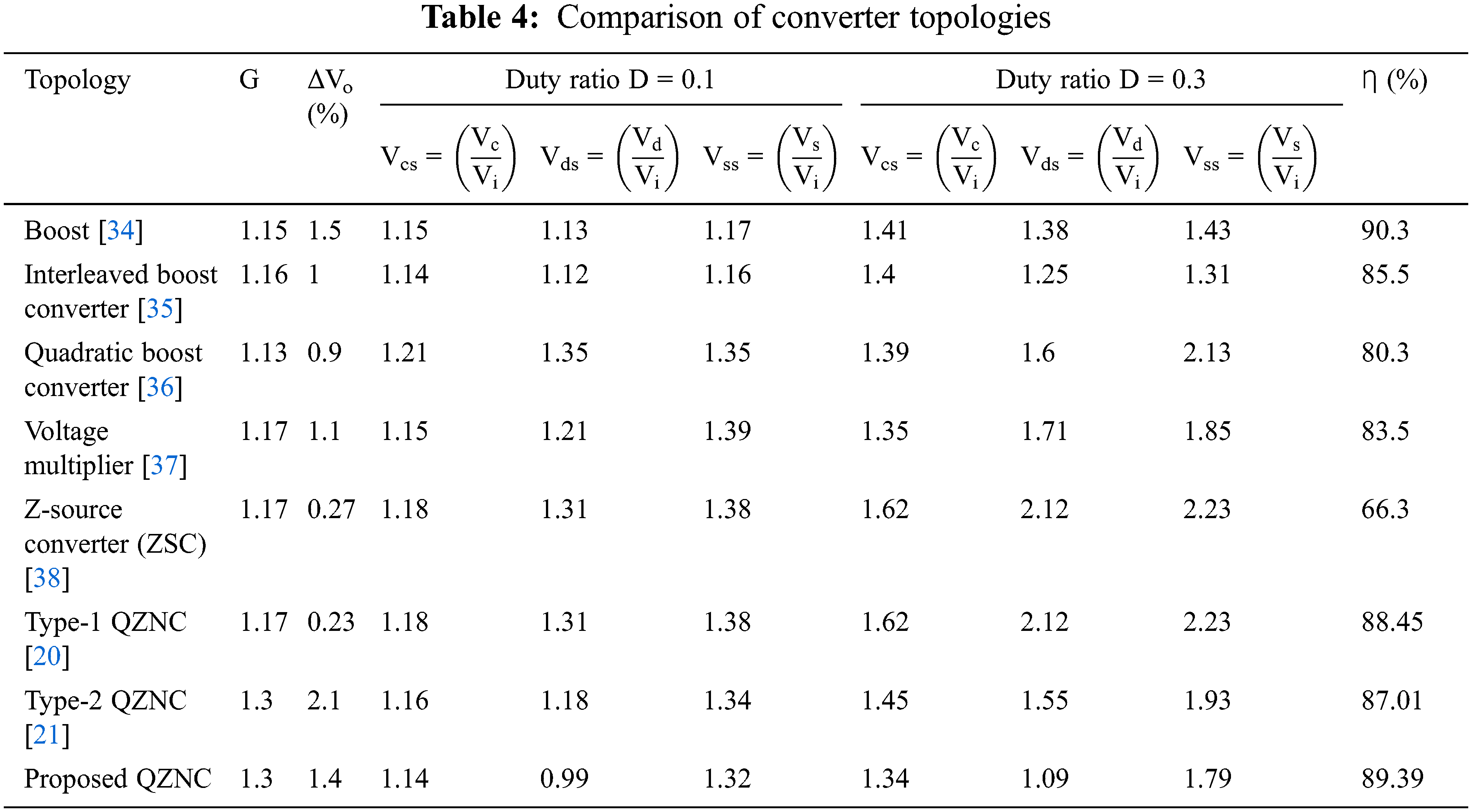

Figure 13: Summary of QZNC
Though Z-source converter has lower ripple in the load voltage as shown in Tab. 4, the stress across the network diode is higher than the boost converter, and efficiency has also reduced. The efficiency has improved with type-1 and type-2 QZNC, still the stress higher and it has limited duty ratio feature. Though the gain of the suggested topology and type-2 converter are same, the gain of the suggested topology is higher than the boost converter, ZSC and type-1 converter. The stress across the network diode has also drastically reduced with the suggested converter (19% reduced) compared with other converter topologies. The reduced load voltage ripple compared with boost converter and the efficiency has enhanced. The stress comparison for two different duty cycles for all the DC-DC converter is listed in Tab. 4. From Tab. 4, it could be implied that the network stress as well as device stress of the recommended topology has reduced even if the duty cycle has increased. Thus, it is observed that the recommended proposed QZNC has better performance as it has high gain, reduced load voltage ripple, reduced network stress and device stress, better efficiency and works well for all the value of duty ratio.
The simulation results also shows that the proposed converter has superior features such as linearly high voltage gain for all the values of duty ratio and reduce voltage spike across the network and device. To validate, a laboratory setup has been developed compared with type-1 and type-2 converter in this section. The setup of proposed QZNC with input of Vin = 40 V, Iin = 1.49 A is depicted in Fig. 14.

Figure 14: Proposed QZNC
The two DC voltage sources cascaded, and it provides 40 V input to the quasi network. From Fig. 14, it could be seen that the boosted voltage is 52.8 V, and the voltage gain is 1.3. The power MOSFET used in the converter is IRFP 840 and diode is FR107. The gating pattern has been generated using ARDUINO UNO. The results measured using power quality analyzer WT500. The waveforms are presented in Figs. 15–18.

Figure 15: Load voltage and load current of proposed QZNC

Figure 16: Network diode voltage waveform
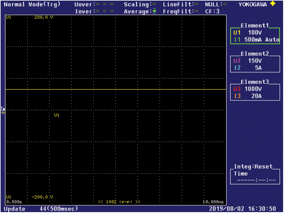
Figure 17: Waveform of the network capacitor voltage

Figure 18: Waveform of the switch voltage
From Figs. 15–18, the measured values are as follows: output voltage ripple is 1.04%. The network diode voltage (Vd) is 4.92 V, network capacitor voltage (Vc) is 43.61 V, device voltage (Vs) is 43.8 V. And, the network diode voltage stress (Vds) is 0.1, network capacitor voltage stress (Vcs) is 1.09 and device voltage stress (Vss) is 1.09.
The comparative analysis between all the three types of converters based on hardware results are presented in the Tab. 5. And the comparison between simulation and hardware results are illustrated in Tab. 6.
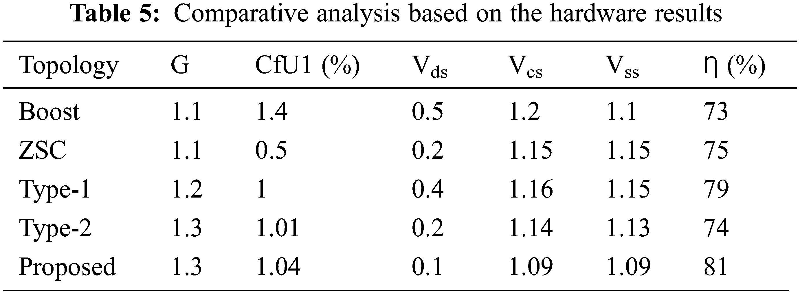
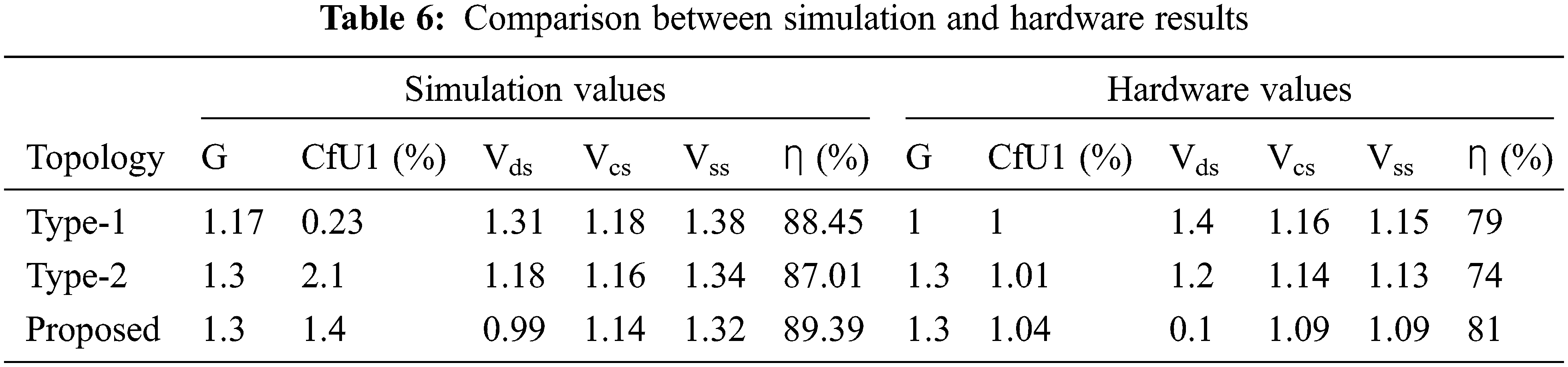
From Tab. 5, it could be inferred that though the voltage gain of proposed QZNC remains same as that of the type-2 converter, but the network and device stress has reduced and the efficiency has improved significantly. Further, it is observed that the variation in the voltage ripple is less compared with the type-2 converter. However, the ripple reduces as the duty ratio increases in the case of the proposed converter as shown in Fig. 7. Therefore, the overall performance of the suggested converter is better than the existing topologies. The comparison between simulation and hardware result is presented in Tab. 6. From 6, it has been concluded that the simulation values are validated through practical results.
In this paper, a new QZNC with low switching noise has been proposed. The problem associated with the existing type-1 and type-2 QZNC is drooping voltage gain profile and higher voltage stress across the impedance network and power device. This has been overcome in the proposed topology using current controlling diode. The working principle and design equations are clearly presented. The performance of the proposed QZNC has been evaluated and compared with the existing topologies such as boost, ZNC, type-1 QZNC and type-2 QZNC. The parameters accounted for analysis are voltage gain, load voltage ripple, capacitor voltage stress, diode voltage stress, device voltage stress, and efficiency. From the analysis, it could be inferred that the suggested converter topology has linearly high voltage gain profile, low load voltage ripple, reduced voltage stress across the network and power device, and higher efficiency. Compared with other topologies, the stress across the network as well as across the devices is reduced with the proposed topology. The laboratory model of the proposed topology has been constructed and evaluated to validate the simulation results. The practical analysis also clearly concludes that the performance of proposed converter is superior to the type-1 and type-2 converter. Hence, the proposed QZNC is suitable for high power applications such as electric vehicle charging station.
Acknowledgement: The authors gratefully acknowledge the SSN Institution for providing computational facilities and S. Harika thanks CSIR for the award of CSIR-SRF (File. No. 08/542/(0009)/19 EMR -I).
Funding Statement: The authors received no specific funding for this study.
Conflicts of Interest: The authors declare that they have no conflicts of interest to report regarding the present study.
References
1. V. Vijayal and K. Krishnamoorthi, “Integrated renewable smart grid system using fuzzy based intelligent controller,” Intelligent Automation & Soft Computing, vol. 33, no. 1, pp. 651–667, 2022. [Google Scholar]
2. D. Sabaripandiyan, H. Habeebullah Sait and G. Aarthi, “A novel hybrid mPPT control strategy for isolated solar PV power system,” Intelligent Automation & Soft Computing, vol. 32, no. 2, pp. 1055–1070, 2022. [Google Scholar]
3. P. Paul, B. R. Jose, T. K. Shahana, C. Abraham and J. Mathew, “High gain isolated quasi-switched boost converter embedded with switched capacitor cell,” Electric Power Components and Systems, vol. 489, no. 4, pp. 333–344, 2021. [Google Scholar]
4. H. S. Son, J. K. Kim, J. B. Lee, S. -S. Moon, J. -H. Park et al., “A new buck-boost converter with low voltage stress and reduced conducting components,” IEEE Transaction on Industrial Electronics, vol. 64, no. 9, pp. 7030–7038, 2017. [Google Scholar]
5. S. Miao, F. Wang and X. Ma, “A new transformerless buck–boost converter with positive output voltage,” IEEE Transaction on Industrial Electronics, vol. 63, no. 5, pp. 2965–2975, 2016. [Google Scholar]
6. A. J. Sabzali, E. H. Ismail and H. M. Behbehani, “High voltage step-up integrated double BoostCSepic DC-DC converter for fuel-cell and photovoltaic applications,” Renewable Energy, vol. 82, no. 5, pp. 44–53, 2015. [Google Scholar]
7. A. Ajami, H. Ardi and A. Farakhor, “A novel high step-up DC/DC converter based on integrating coupled inductor and switched-capacitor techniques for renewable energy applications,” IEEE Transaction on Power Electronics, vol. 30, no. 8, pp. 4255–4263, 2015. [Google Scholar]
8. H. Bahrami, E. Adib, S. Farhangi, H. Iman-Eini and R. Golmohammadi, “ZCS-PWM interleaved boost converter using resonance-clamp auxiliary circuit,” IET Power Electronics, vol. 10, no. 3, pp. 405–412, 2017. [Google Scholar]
9. H. Fathi and H. Madadi, “Enhanced-boost Z-source inverters with switched Z-impedance,” IEEE Transaction on Industrial Electronics, vol. 63, no. 2, pp. 691–703, 2016. [Google Scholar]
10. G. Zhang, H. H. C. Iu, B. Zhang, Z. Li, T. Fernando et al., “An impedance networks boost converter with high-voltage gain,” IEEE Transaction on Power Electronics, vol. 32, no. 9, pp. 6661–6665, 2017. [Google Scholar]
11. H. Liu, Y. Ji, L. Wang and P. Wheeler, “A family of improved magnetically coupled impedance network boost DC–DC converters,” IEEE Transactions on Power Electronics, vol. 33, no. 5, pp. 3697–3702, 2018. [Google Scholar]
12. M. R. Banaei and H. A. F. Bonab, “A high efficiency non-isolated buck–boost converter based on ZETA converter,” IEEE Transactions on Industrial Electronics, vol. 67, no. 3, pp. 1991–1998, 2020. [Google Scholar]
13. A. Tahavorgar and J. E. Quaicoe, “A dual series-resonant DC–DC converter,” IEEE Transaction on Power Electronics, vol. 32, no. 5, pp. 3708–3718, 2017. [Google Scholar]
14. J. Liu, J. Wu, J. Qiu and J. Zeng, “Switched Z-source/Quasi-Z-source DC-DC converters with reduced passive components for photovoltaic systems,” IEEE Access, vol. 7, no. 2, pp. 40893–40903, 2019. [Google Scholar]
15. Y. Liu, H. A. Rub and B. Ge, “Front-end isolated Quasi-Z-source DC–DC converter modules in series for high-power photovoltaic systems—Part I: Configuration, operation, and evaluation”, IEEE Transactions on Industrial Electronics, vol. 64, no. 1, pp. 347–358, 2017. [Google Scholar]
16. M. Karimi, M. Mahdavi and A. T. Harchegani, “A new soft switching QZSC converter by using coupled inductor,” Electric Power Components and Systems, vol. 46, no. 3, pp. 270–277, 2018. [Google Scholar]
17. Y. P. Siwakoti, F. Z. Peng, F. Blaabjerg, P. C. Loh and G. E. Town, “Impedance source network for electric power conversion—Part I : A topological review,” IEEE Transaction on Power Electronics, vol. 30, no. 2, pp. 699–716, 2015. [Google Scholar]
18. Y. Liu, H. A. Rub, B. Ge, F. Blaabjerg, O. Ellabban et al., Impedance source power electronic converters, U.K.: Wiley, 2016, https://ieeexplore.ieee.org/book/7572256. [Google Scholar]
19. Y. P. Siwakoti, F. Blaabjerg and P. C. Loh, “New magnetically coupled impedance (Z-) source networks,” IEEE Transaction on Power Electronics, vol. 31, no. 11, pp. 7419–7435, 2015. [Google Scholar]
20. G. Zhang, B. Zhang, Z. Li, D. Qiu, L. Yang et al., “A 3-Z-network boost converter,” IEEE Transaction on Industrial Electronics, vol. 62, no. 1, pp. 278–288, 2015. [Google Scholar]
21. E. Liivik, A. Chub and D. Vinnikov, “Efficiency improvement from topology modification of the single-switch isolated Quasi-Z-source DC-DC converter,” in 57th Int. Scientific Conf. on Power and Electrical Engineering of Riga Technical University (RTUCON), Riga, Latvia, Oct 13, pp. 1–7, 2016. [Google Scholar]
22. R. V. Silva, A. A. A. Freitas, M. R. Castro, F. L. M. Antunes and E. M. Sá, “High gain QZS DC/DC converter with coupled inductor,” in IEEE Applied Power Electronics Conf. and Exposition (APEC), Long Beach, CA, USA, Mar 20, pp. 2592–2598, 2016. [Google Scholar]
23. A. Chub, D. Vinnikov, F. Blaabjerg and F. Z. Peng, “A review of galvanically isolated impedance-source DC-DC converters,” IEEE Transaction on Power Electronics, vol. 31, no. 4, pp. 2808–2828, 2016. [Google Scholar]
24. L. Yang, D. Qiu, B. Zhang, G. Zhang and W. Xiao, “A Quasi-Z-source DC-DC converter,” in IEEE Energy Conversion Congress and Exposition (ECCE), Pittsburgh, PA, USA, Nov 13, pp. 941–947, 2014. [Google Scholar]
25. X. Zhu and B. Zhang, “High step-up Quasi-Z-source DC–DC converters with single switched capacitor branch,” Journal of Modern Power System and Clean Energy, vol. 5, no. 4, pp. 537–547, 2017. [Google Scholar]
26. A. M. S. S. Andrade and R. A. Guisso, “Quasi-Z-source network DC–DC converter with different techniques to achieve a high voltage gain,” Electronics Letters, vol. 54, no. 11, pp. 710–712, 2018. [Google Scholar]
27. A. Chub and D. Vinnikov, “Single-switch galvanically isolated Quasi-Z-source DC-DC converter,” in IEEE Int. Conf. on Power Engineering, Energy and Electrical Drives (POWERENG), Riga, Latvia, May 11, pp. 582–586, 2015. [Google Scholar]
28. A. Kumar and R. K. Singh, “Power loss calculation of diode assisted cascaded Quasi-Z-source converter with CCM and DCM operation,” in IEEE 6th Int. Conf. on Power Systems (ICPS), New Delhi, India, Mar. 4, pp. 1–6, 2016. [Google Scholar]
29. J. Zeng, J. Wu, Z. Yu and J. Liu, “Switched Z-source DC-DC converter,” in IECON 43rd Annual Conf. of the IEEE Industrial Electronics Society, Beijing, China, Dec 18, pp. 8039–8044, 2017. [Google Scholar]
30. L. Yang, D. Qiu, B. Zhang, G. Zhang and W. Xiao, “A modified Z-source DC-DC converter,” in European Conf. on Power Electronics and Applications, Lappeenranta, Aug 26, pp. 1–9, 2014. [Google Scholar]
31. M. K. Thangavel, B. K. Ramasamy and P. Ponnusamy, “Performance analysis of dual space vector modulation technique-based quasi Z-source direct matrix converter”, Electric Power Components and Systems, vol. 48, no. 11, pp. 1185–1196, 2020. [Google Scholar]
32. E. S. Asl and M. Sabahi, “A class of Quasi-Cuk DC/DC converters: Steady-state analysis and design,” Electric Power Components and Systems, vol. 46, no. 5, pp. 581–599, 2018. [Google Scholar]
33. A. Singh, A. Kumar, A. R. Gupta and R. K. Singh, “Steady state analysis of Quasi switched boost DC-DC converter in CCM,” in IEEE Int. Conf. on Power Electronics, Intelligent Control and Energy, Delhi, India, Jul 4, pp. 1–6, 2016. [Google Scholar]
34. S. Masri and P. W. Chan, “Design and development of a DC-DC boost converter with constant output voltage,” in Int. Conf. on Intelligent and Advanced Systems, Kuala Lumpur, Malaysia, June 15, pp. 1–4, 2010. [Google Scholar]
35. J. Guo, R. Rodriguez, J. Gareau, D. Schumacher, M. Alizadeh et al., “A comprehensive analysis for high-power density, high-efficiency 60 kW interleaved boost converter design for electrified powertrains,” IEEE Transactions on Vehicular Technology, vol. 69, no. 7, pp. 7131–7145, 2020. [Google Scholar]
36. M. Veerachary and N. Kumar, “Analysis and design of quadratic following boost converter,” IEEE Transactions on Industry Applications, vol. 56, no. 6, pp. 6657–6673, 2020. [Google Scholar]
37. K. Sreeram, “An improvised voltage multiplier circuit for industrial applications and grids,” in 2018 Int. Conf. on Circuits and Systems in Digital Enterprise Technology (ICCSDET), Kottayam, India, sept 2, pp. 1–5, 2018. [Google Scholar]
38. H. Shen, B. Zhang and D. Qiu, “Hybrid Z-source boost DC–DC converters,” IEEE Transaction on Industrial Electronics, vol. 64, no. 1, pp. 310–319, 2017. [Google Scholar]
Cite This Article
 Copyright © 2023 The Author(s). Published by Tech Science Press.
This work is licensed under a Creative Commons Attribution 4.0 International License , which permits unrestricted use, distribution, and reproduction in any medium, provided the original work is properly cited.
 Downloads
 Citation Tools