
 Submit a Paper
 Propose a Special lssue
 Open Access
ARTICLE
IC Pattern Based Power Factor Maximization Model for Improved Power Stabilization
1 R.M.K. College of Engineering and Technology, Thiruvallur, 601206, India
2 R.M.K. Engineering College, Thiruvallur, 601206, India
* Corresponding Author: N. Hariharan. Email:
Intelligent Automation & Soft Computing 2023, 36(1), 401-414. https://doi.org/10.32604/iasc.2023.030768
Received 01 April 2022; Accepted 25 May 2022; Issue published 29 September 2022
 View Full Text
 Download PDF
Abstract
The voltage fluctuation in electric circuits has been identified as key issue in different electric systems. As the usage of electricity growing in rapid way, there exist higher fluctuations in power flow. To maintain the flow or stability of power in any electric circuit, there are many circuit models are discussed in literature. However, they suffer to maintain the output voltage and not capable of maintaining power stability. To improve the performance in power stabilization, an efficient IC pattern based power factor maximization model (ICPFMM) in this article. The model is focused on improving the power stability with the use of IC (Inductor and Conductor) towards identifying most efficient circuit for the current duty cycle according to the input voltage, voltage in capacitor and output voltage required. The model with boost converter diverts the incoming voltage through number of conductors and inductors. By triggering specific inductor, a specific capacitor gets charged and a particular circuit gets on. The model maintains number of IC (Inductor and Conductor) patterns through which the power flow occurs. According to that, the pattern available, the mofset controls the level of power to be regulated through any circuit. From the pattern, the model computes the Circuits Switching Loss and Circuits Conduction Loss for various circuits. According to the input voltage, the model estimates Circuit Power Stabilization Support (CPSS) according to the voltage available in any capacitor and input voltage. Using the value of CPSS, the model trigger optimal number of circuits to maintain voltage stability. In this approach, more than one circuit has been triggered to maintain output voltage and to get charged. The proposed model not only maintains power stability but also reduces the wastage in voltage which is not utilized. The proposed model improves the performance in voltage stability with less switching loss.Keywords
The electric power has been identified as the keen entity and source which has higher importance in modern world. The uses of electric and electronic devices are getting increased every day and the electric power is the source being used for the functioning of such systems. The electric power is the energy being generated from limited source like coal, water and wind in form of thermal, atomic, wind and sunlight. However, the electric power is generated from number of sources, the wind source is available for limited period of year and it varies in different region. Similarly, the thermal power is generated from water and coal which are precious and available in limited volume. All these increase the importance of using the electric power being generated from any source with efficient manner.
In general the power or electricity being circulated through any circuit would loss certain amount of voltage. Such voltage loss is due to the conduction and other devices. Such loss should be reduced to get higher voltage. In many designs of circuits and power model, there will be higher voltage loss and the output voltage gets reduced. For any electric system, it requires steady and higher voltage according to the requirement. To maintain the power stability, there are number of stabilization models exist in literature. Towards this, there are number of converters exist to support the problem but suffer with higher voltage and switching loss. The Direct Current-Direct Current (DC-DC) converters are highly efficient in maintaining the output voltage which is capable of converting the direct current into direct current. However, the existing models suffer to achieve higher output voltage.
The block diagram of general DC-DC boost converter is presented in Fig. 1, which receives the input voltage and maximize the voltage to increase the output voltage.
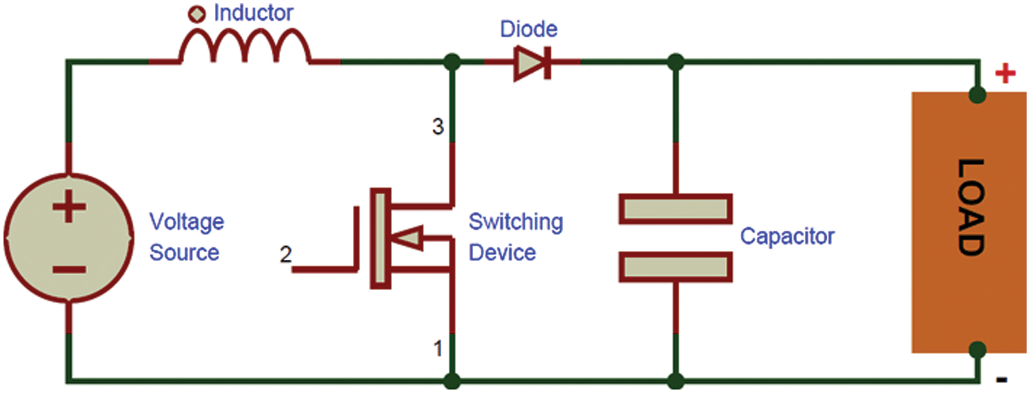
Figure 1: General block diagram of DC-DC boost converter
The block diagram of DC-DC converter with controller is presented in Fig. 2, which controls the flow of voltage according to the input voltage to maximize the output voltage. The converter converts the direct current into direct current where the presence of rectifier increases or decreases the voltage flow to meet the output requirement.
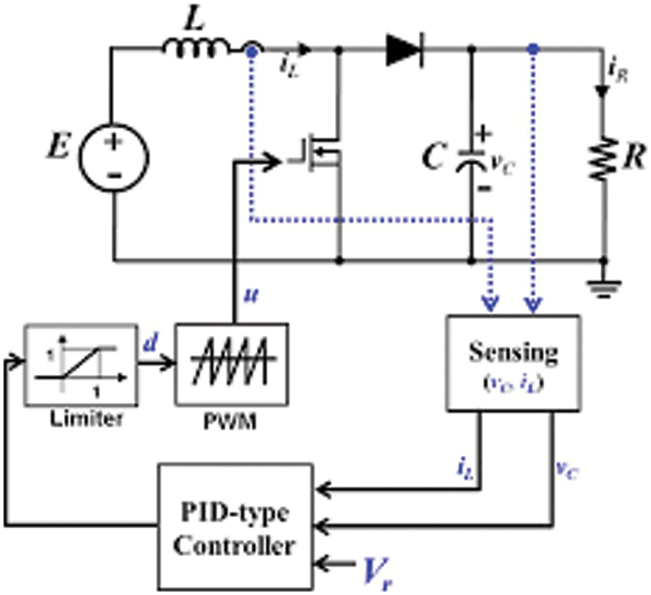
Figure 2: Block diagram of Boost DC-DC converter with controller
The power stabilization is the process of maintaining the output voltage of any power model. The input power or voltage would be varying according to different conditions like conduction and generation. However, the end system would require steady voltage to function in proper way. The stabilization model has the responsibility in maintaining the output voltage and such activity has been performed by several models but suffers to achieve higher performance. On the other side, the most models switch only unique circuit at a time which introduces higher voltage loss. By considering this, an efficient model is designed which is capable of switching the input voltage into different circuits according to the conditions of capacitors and inductors in different circuits. However, the switching and conduction process introduces voltage loss which must be considered at the designing of power stabilization model.
Towards maintaining higher and steady voltage, and Real Time IC Pattern Based Power Factor Maximization Model for Improved Power Stabilization Using Boost Rectifiers is designed in this paper. The model works based on the inverter and converter pattern which represent the pattern of inverter and converter being switched to on at any cycle. As the model has different integrated circuits where each has an inverter and converter with metal-oxide-semiconductor field-effect transistor (MOFSET) attached, the IC pattern describes which inverter and converter are switched to ON condition at any duty cycle considered.
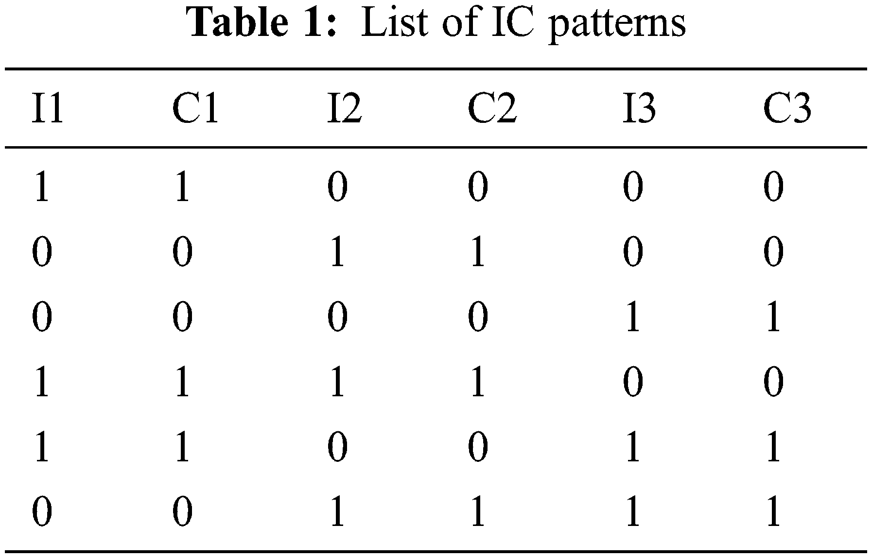
Consider the stabilization model S with K number of circuit with K number of inductor and capacitors; we can generate 2K number of patterns from the model, where each circuit has its own capacitor and inductor. For example when there exist 3 circuits, then you can generate the patterns as follows:
The list of IC patterns can be generated from the circuit has been presented in Tab. 1, which represents the set of inductor and capacitors being switched on at any duty cycle is presented. According to the IC patterns and the voltage at different capacitors, the circuit selection and triggering can be performed. By switching the voltage under different circuit, the performance of power stabilization can be improved. With the use of IC patterns, the model can identify most optimal and suitable circuit to be triggered for any duty cycle which would reduce the loss as well as maintain the voltage flow to meet output voltage. The detailed approach is discussed in detail in the next section.
There are number of approach are recommended in literature towards power stabilization and such approaches are discussed in detail.
To maintain the voltage stability in micro grids, and controller is designed which uses sliding mode to regulate the voltage according to the input volt combination and resistive load. The controller designed works to maintain the power supply for the application considered [1]. The value of duty cycle has higher importance in power regulation in different controllers and according to that a feedback orient circuit is fabricated to adjust the duty cycle values which generate stability in output voltage at different input conditions [2]. On the other side, an active model is designed to maintain the output voltage in a stable mode [3].
The stability in maintaining the output voltage in any DC converter is depending on various input patterns. In [4], an efficient predictive model is presented which monitor different incoming voltage values and according to the average value produced at different duty cycles. The model reduces the space complexity of capacitors and suitable for low power models [5].
A novel PCC is designed which works based on non-inverting buck boost converter to maintain higher voltage [6], which reduces the value of capacitance. On the other side, a DC/DC model is fabricated which works according to two step digital pulse width modulation and capable of detecting zero current. The converter is suitable to be adapted for IoT devices and Digital Power Management (DPWM) model shows least power consumption [7].
Towards achieving higher conversion efficiency, a hysteresis control scheme orient converter is modeled in [8], which uses frequency scaling and achieves higher conversion efficiency. Also, a two stage GCPVS is modeled on cuk converter and uses incremental conductance algorithm to track maximum power point [9].
Towards maximizing output power a cuk DC/DC converter is designed and shows the resistance on various loads with MPPT controller [10]. Similarly, an integrated cuk converted with feed forward model is designed in which uses solar energy to generate the voltage and pass through photo voltaic cells to store them [11]. The application of fuzzy logic is used in cuk converter in which adapts micro inverters to maintain the output voltage. Also, the model selects the passive component according to the ripple value [12]. A pseudo DC link based module integrated solar micro-inverter is presented in [13], which can extract the solar power individually for the maximum from every PV panel to transfer the power to AC system. The model is designed to achieve higher conversion efficiency with various link topology. In [14], a future renewable electric energy delivery and management (FREEDM) system is presented which enables a dc interface to obtain alternate source of energy. The energy from the PV system can be passed through dc/dc converter to the FREEDM system’s dc bus. The module-integrated converter (MIC) topology is a good candidate for a PV converter designed to work with the FREEDM system. The problem of calculating the mean time between failures (MTBF) is handled with photovoltaic module-integrated inverter (PV-MII) in [15], which works according to the stress-factor reliability methodology and applies a usage model for the inverter to determine the statistical distribution of thermal and electrical stresses for the electrical components. The proposed methodology is used to examine the reliability of six different candidate inverter topologies for a PV-MII. In [16], a mixed-integer algorithm for the optimal dispatch of power is designed which works according to the day ahead PV forecasting. The method works based on the active power profile defined by the operator. In [17], a cooperative operation framework model for a Wind-Solar-CCHP Multi-energy system is defined. The Nash Bargaining problem is optimized to solve energy trading and social welfare maximization problem.
Problem Statement
According to the literature survey, the existing models and converters consider only the output voltage required and switches different circuits to meet the requirement. However, the most input voltage gets lost due to the poor selection of circuit. Because of poor selection of circuits and triggering single circuit for voltage support, introduces higher switching loss. This entirely affects the performance of power stabilization and voltage regulation. Because, if the input voltage is even near to the output voltage, the models does not trigger the other circuits to get charged and they look on maintaining the output voltage at current duty cycle but does not consider the next cycles. This must be considered and the other circuits must be charged to support in the future cycles.
3 Real Time IC Pattern Based Power Factor Maximization Model
The proposed IC pattern based power factor maximization model has number of circuits integrated in series where each circuit has capacitor and inductor. The model has dedicated MOFSET attached to each of the circuit which controls the flow of voltage to the circuit. Also, the method maintains the list of circuits being triggered in each duty cycle with the voltage available in each capacitors of the circuit. In each duty cycle, the method generates number of IC pattern and for each of them the method computes the value of circuit power stabilization support (CPSS) based on which a different circuits are selected. Selected circuits are triggered to get charged and discharge towards achieving expected output voltage. The detailed functioning is presented in this section.
The functional architecture of proposed IC pattern based power factor maximization model is presented in Fig. 3, where the functional components are detailed in this section. The proposed ICPFMM model continuously monitors the input voltage and output voltage required. With the details of voltage resident in each circuit and input voltage, the model would select most optimal circuit to support the output voltage and triggers few other circuits to get charged to support in the future cycle. It involves in IC pattern generation which generates number of sequence of circuits and estimates CPSS values for each pattern. According to the value of CPSS, the model would perform circuit selection to enforce power stabilization in the model.
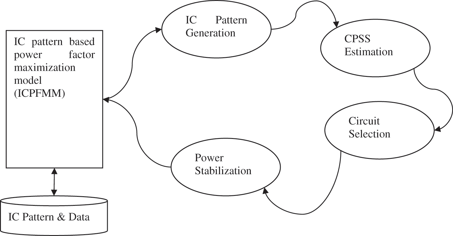
Figure 3: Architecture of proposed ICPFMM model
The inductor and capacitor pattern is generated towards maintaining the voltage stability in the circuit. To generate the pattern, first the method identifies the list of circuits available. In each circuit, the inductor and capacitor available are identified. Using all these, the method generates possible combination of sequences of circuit as pattern. According to the patterns of circuit generated, the method finds the last few circuit pattern and eliminate them from the list. Such pattern set generated has been used towards voltage stabilization to improve the voltage stability.
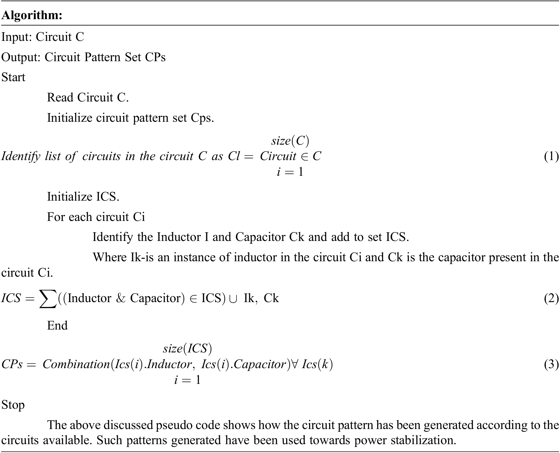
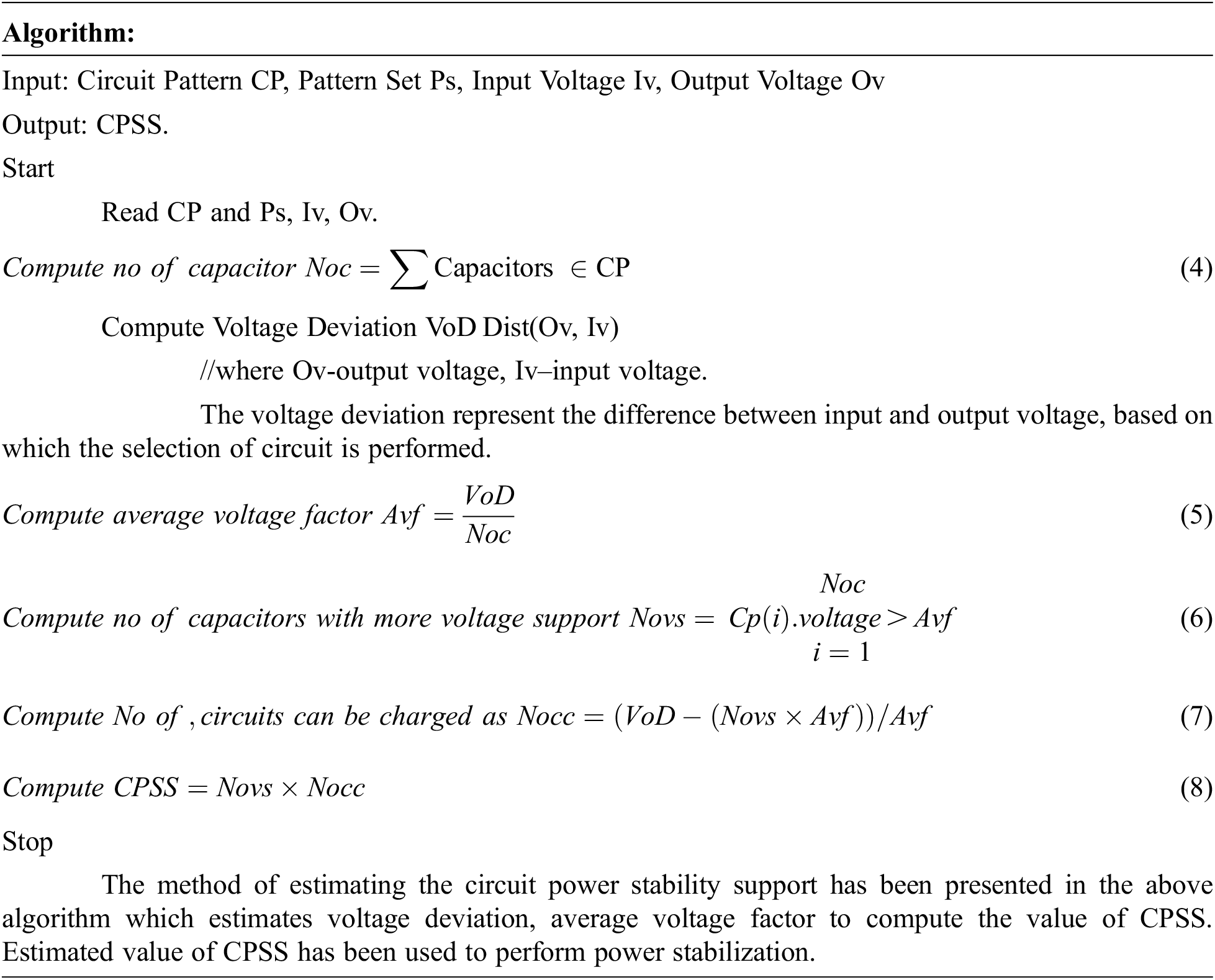
The circuit pattern stabilization support is the measure which represents the performance of any circuit pattern in maintaining the power stability. Any circuit would contain an inductor and capacitor. Similarly, in any pattern of circuit, there will be number of inductor and capacitor, available. Each capacitor would store certain amount of voltage and by triggering all the circuits, the voltage present in the circuit would be used to achieve the output voltage. The value of CPSS is measured according to the number of capacitors having voltage which is more than the average voltage induction to be generated and the number of capacitors present in the circuit. Also, the number of circuits can be triggered for charging with the input voltage in the current duty cycle with the output voltage required. The value of CPSS has been used in the selection of circuit pattern towards stabilization model.
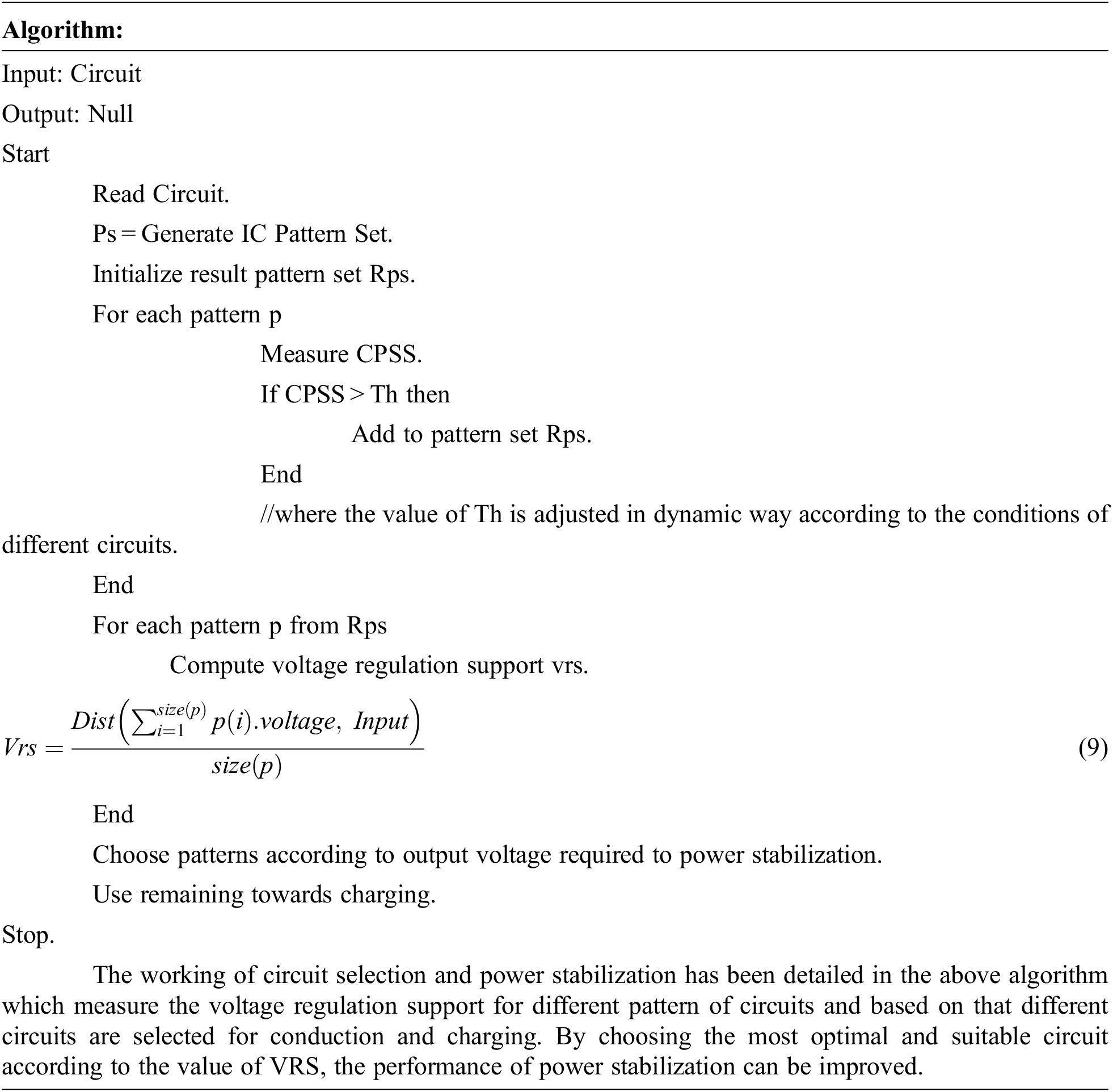
3.3 Circuit Selection and Power Stabilization
The proposed power stabilization model keeps track of circuit being triggered at different time stamp. The method first identifies the set of circuits and capacitors/inductors available in the circuit. According to the components and circuits identified, the method generates the pattern set of circuits. For each pattern, the method estimates the CPSS measure and based on that the pattern with maximum CPSS value has been selected as the circuit to be triggered. For the circuit pattern being selected, the method selects top few circuit patterns and the most one is used to regulate the voltage where the remaining are used to get charged. The method estimates the voltage regulation support (VRS) for different patterns and according to the required voltage, a set of circuits are triggered and remaining are triggered for charging.
The proposed real time IC pattern based power factor maximization model (ICPFMM) has been structured and fabricated towards simulating in matrix laboratory (MATLAB) tool. The performance of the power stabilization model has been evaluated under different parameters.
The circuit diagram of ICPFMM model is presented in Fig. 4, which contains number of circuits and each has their own inductor and capacitors with dedicated MOFSET to control the voltage.
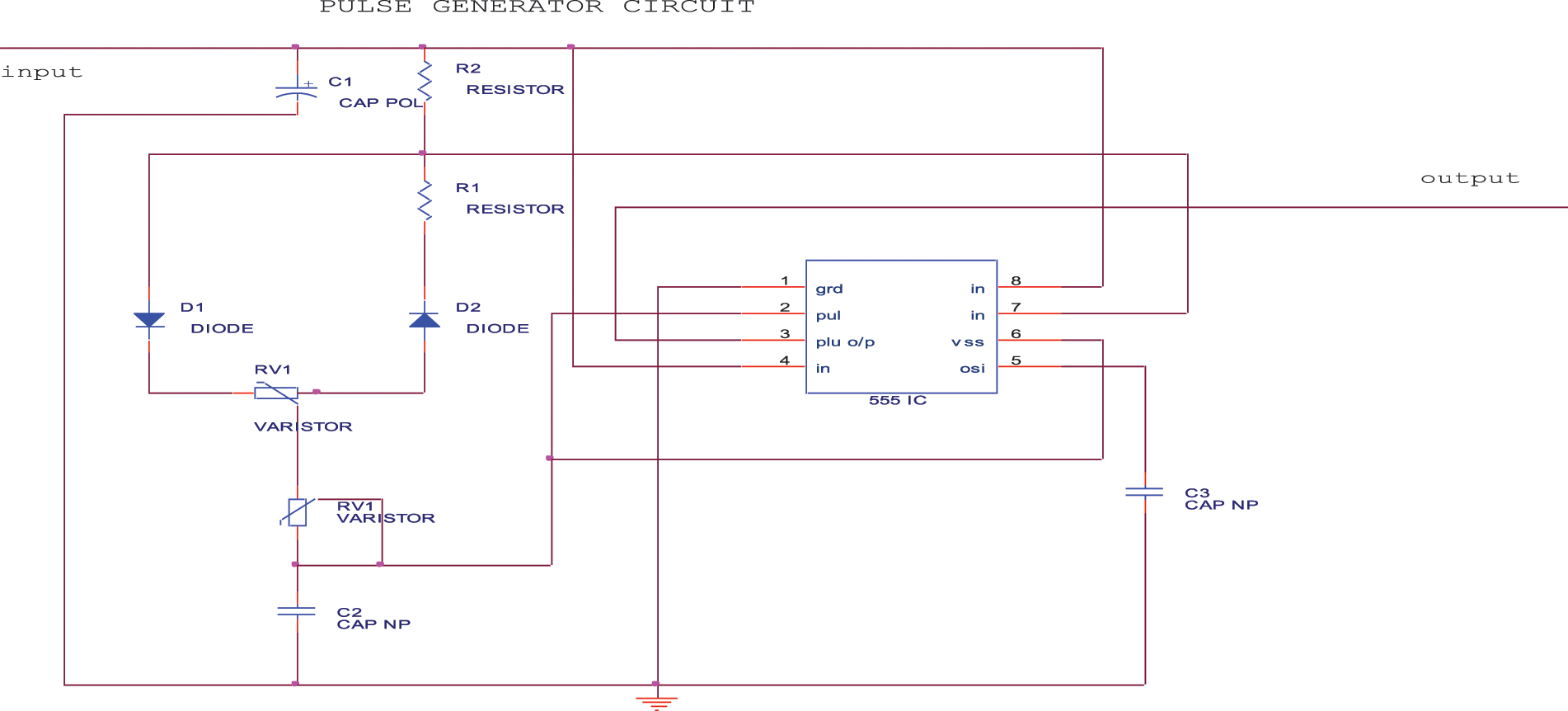
Figure 4: Circuit diagram of ICPFMM model
The model contains unique inductor and capacitor where any inductor could store power in the ratio as follows:
Similarly, the amount of voltage being regulated in any inductor can be measured as follows:
The inductor I1 in the circuit and the capacitor C are being connected in a serial mode. So that the value of voltage being discharged is measured as below:
where Vi is the input voltage, Vo is the output voltage, Vc is the voltage at the capacitor, V(I1) is the voltage at the inductor and V(I2) is the voltage at the inductor I2.
The voltage concern in any inductor I1 and I2 are measured based on Eq. (14) and (15) where each of them are connected with capacitor and load.
Using these two equations and values, the value of average current which pass through the inductors I1 and I2 can be measured as below:
Voltage available across the inductor L1
where D = Duty cycle.
Vout = output voltage. Vin = input voltage.
VI = inductance voltage. VC = capacitance voltage.
The above scenario is the manipulation of two different circuits which can be approximated for N number of circuits in a series. The number of IC pattern can be generated is restricted according to the total number of circuits available. Consider a pattern P which has been generated according to the values of Tab. 1, then the output voltage for the pattern p can be measured as follows.
where the voltage available at the Inductor Ik is the value of voltage available in the capacitance Ck and the previous capacitance in the pattern P. By summing all the voltages, the value of output voltage can be measured.
The wave form of voltage input and Input current generated by the simulator is presented in Figs. 5 and 6. Also, the voltage output and current has been measured and displayed in Figs. 7 and 8.
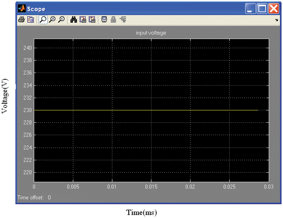
Figure 5: Input voltage
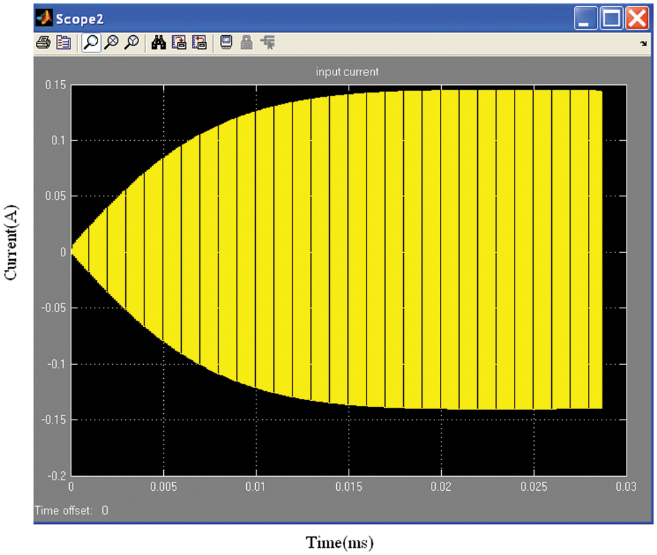
Figure 6: Input current
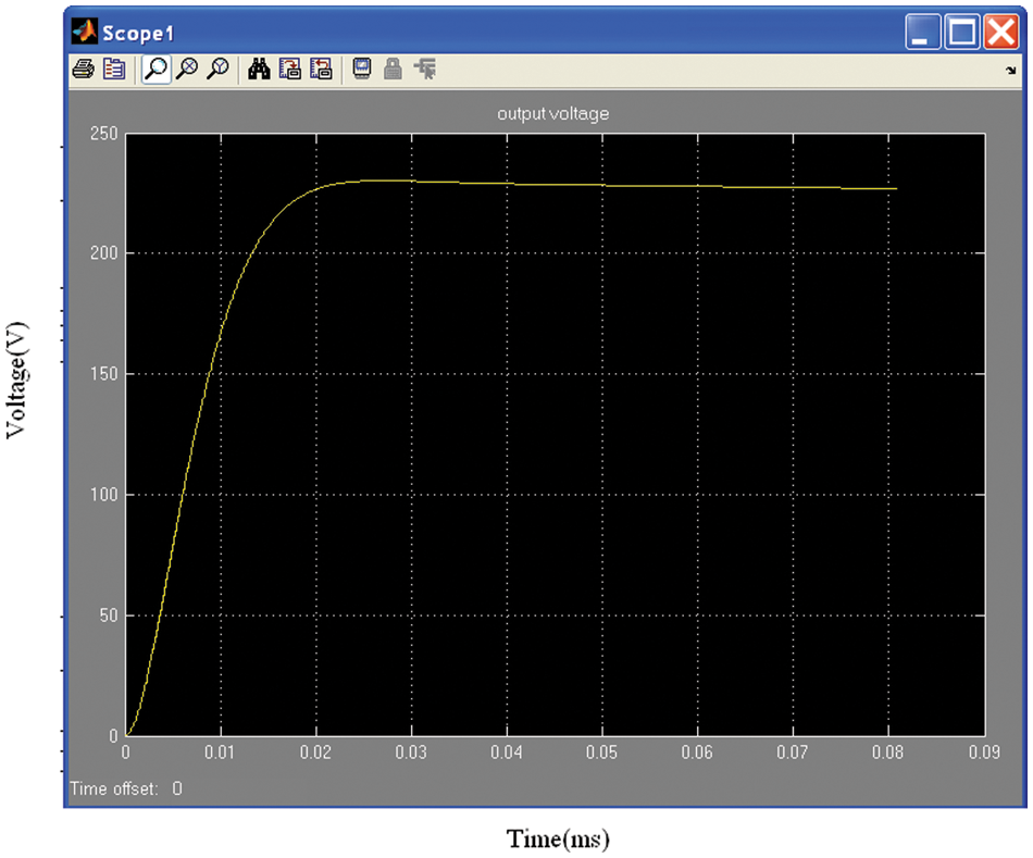
Figure 7: Output voltage
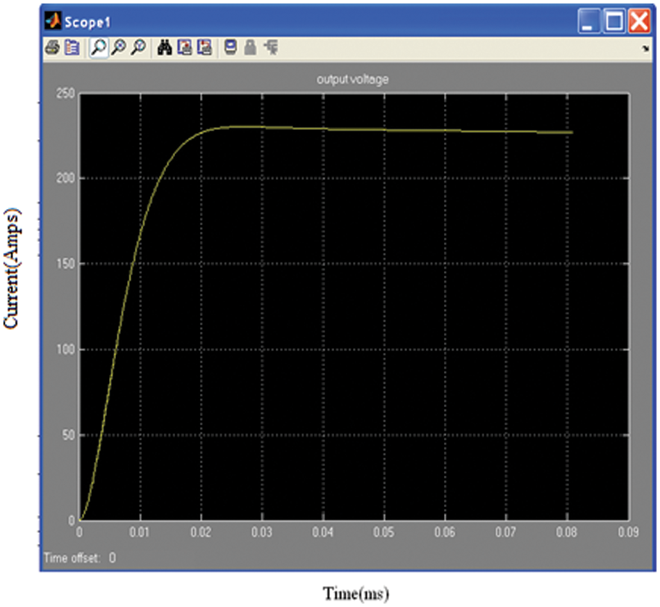
Figure 8: Output current
The Figs. 7 and 8 represents the performance development in power stabilization by the proposed model which is measured for the input current with 230 amps.
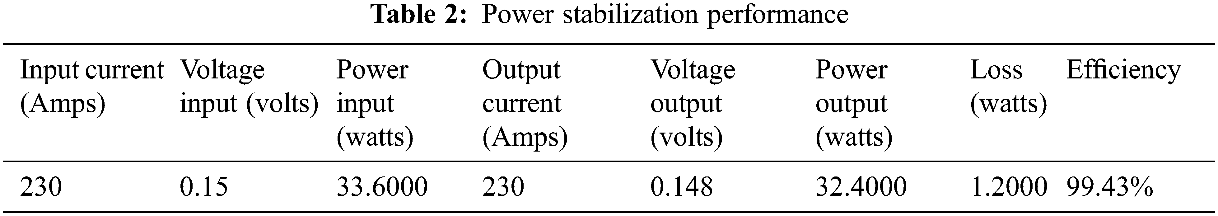
The performance of power stabilization produced by the proposed model is evaluated and plotted in Tab. 2. The proposed model has achieved higher stabilization.
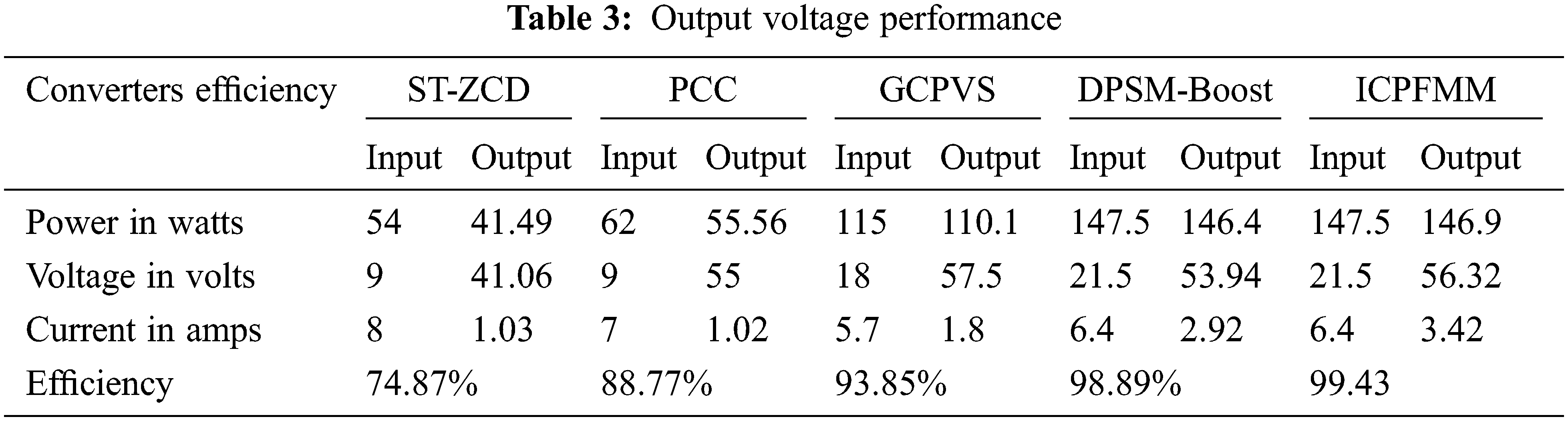
The efficiency in producing higher output voltage by various models are measured and presented in Tab. 3. The ICPFMM model produced higher output voltage performance compare to various approaches.
The efficiency of ICPFMM model has been evaluated towards output voltage and displayed in Fig. 9. The proposed model has produced higher performance.
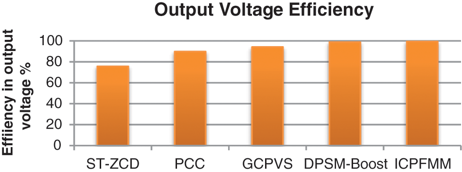
Figure 9: Analysis on output voltage efficiency
The loss ratio produced by different models are measured and presented in Fig. 10. The ICPFMM model produced less loss ratio.
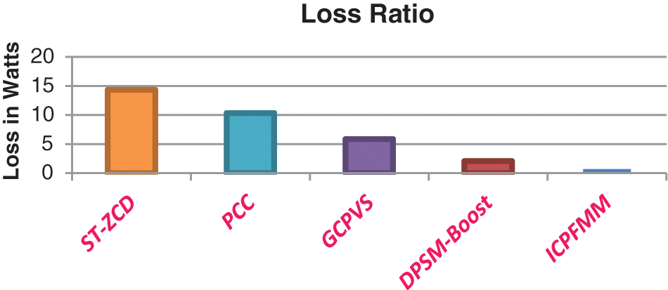
Figure 10: Analysis on loss ratio
In this paper, an efficient real time IC pattern based voltage stabilization model with buck boost converter is designed. The model maintains number of IC (Inductor and Conductor) patterns through which the power flow occurs. According to that, the pattern available, the mofset controls the level of power to be regulated through any circuit. From the pattern, the model computes the Circuits Switching Loss and Circuits Conduction Loss for various circuits. According to the input voltage, the model estimates Circuit Power Stabilization Support (CPSS) according to the voltage available in any capacitor and input voltage. Using the value of CPSS, a single or multiple circuits are triggered to regulate stable voltage. In this approach, more than one circuit has been triggered and controlled to regulate the output voltage and to get charged. The proposed model improves the performance of voltage regulation up to 99.43% with reduced loss ratio 0.57. In future, the same problem can be handled by adapting genetic algorithm in circuit selection which can mutate number of circuits to which the model can measure the suitability measures to support power stabilization.
Funding Statement: The authors received no specific funding for this study.
Conflicts of Interest: The authors declare that they have no conflicts of interest to report regarding the present study.
References
1. S. Singh, “Voltage regulation and stabilization of DC/DC buck converter under constant power loading,” in Proc. IEEE Int. Conf. on Power Electronics, Drives and Energy Systems, IIT, Bombay, India, 2014. [Google Scholar]
2. B. Budiman, “Stabilization of output voltage with feedback circuit and filter on 2 stages-step up converter (24 V to 312 V DC),” in IOP Conf. Series: Materials Science and Engineering, Bandung, Indonesia, 2017. [Google Scholar]
3. O. Lorzadeh, “A novel active stabilizer method for DC/DC power converter systems feeding constant power loads,” in Proc. IEEE 28th Int. Symp. on Industrial Electronics, Vancouver, BC, Canada, 2019. [Google Scholar]
4. A. Mortinez, “Nonlinear model predictive stabilization of DC-DC boost converters with constant power loads,” IEEE Journal of Emerging and Selected Topics in Power Electronics, vol. 9, no. 1, pp. 822–830, 2020. [Google Scholar]
5. M. Shwetha and S. Lakshmi, “DC-DC buck boost converter for renewable and biomedical application based real-time IoT,” International Journal of Recent Technology and Engineering, vol. 8, no. 4, pp. 822–830, 2019. [Google Scholar]
6. D. Li, Z. Gong, M. Rose, H. Bergveld and O. Trescases, “Improved dynamics in DC-DC converters for iot applications with repetitive load profiles using self-calibrated preemptive current control,” in IEEE Applied Power Electronics Conf. and Exposition, Tampa, FL, USA, pp. 3352–3356, 2017. [Google Scholar]
7. S. Y. Kim, Y. J. Park, I. Ali, T. T. K. Nga, H. C. Ryu et al., “Design of a high efficiency DC–DC buck converter with two-step digital PWM and low power self-tracking zero current detector for IoT applications,” IEEE Transactions on Power Electronics, vol. 33, pp. 1428–1439, 2018. [Google Scholar]
8. C. S. Wu, M. Takamiya and T. Sakurai, “Clocked hysteresis control scheme with power-law frequency scaling in buck converter to improve light-load efficiency for IoT sensor nodes,” IEEE Transactions on Very Large Scale Integration Systems, vol. 26, pp. 1139–1150, 2018. [Google Scholar]
9. M. S. Syam, “Grid connected PV system using cuk converter,” in Proc. Int. Conf. on Microelectronics, Communications and Renewable Energy, Kanjirapally, India, 2013. [Google Scholar]
10. M. Habib Ullah, “Design and performance analysis of a PV system with MPPT cuk converter in varying load resistance using matlab,” in Proc. Int. Conf. on Engineering Research, Innovation and Education, Sylhet, Bangladesh, 2013. [Google Scholar]
11. B. R. Lin, “Integrated cuk-forward converter for photovoltaic-based LED lighting,” International Journal of Electronics, vol. 96, no. 9, pp. 943–959, 2009. [Google Scholar]
12. R. Deebika, “Simulation of photovoltaic based grid connected micro inverter using cuk converter,” International Journal of Innovative Research in Science, Engineering and Technology, vol. 3, no. 1, pp. 1001–1007, 2014. [Google Scholar]
13. H. Jen Chiu, Y. Kang Lo, C. Yu Yang and S. Jen Cheng, “A Module-integrated isolated solar microinverter,” IEEE Transactions on Industrial Electronics, vol. 60, no. 2, pp. 781–788, 2012. [Google Scholar]
14. Z. Iang, R. Guo, J. Li and Q. Huang, “A High-efficiency pv module-integrated DC/DC converter for PV energy harvest in freedm systems,” IEEE Transactions on Power Electronics, vol. 26, no. 3, pp. 897–909, 2011. [Google Scholar]
15. S. Harb and S. Balog, “Reliability of candidate photovoltaic module-integrated-inverter (PV-MII) topologies-a usage model approach,” IEEE Transactions on Power Electronics, vol. 28, no. 6, pp. 3019–3027, 2013. [Google Scholar]
16. F. Conte, F. D. Agostino, P. Pongiglione, M. Saviozzi and F. Silvestro, “Mixed-integer algorithm for optimal dispatch of integrated PV-storage systems,” IEEE Transactions on Industry Applications, vol. 55, no. 1, pp. 238–247, 2019. [Google Scholar]
17. M. Yunshou, W. Jiekang, C. Zhihong, W. Ruidong, Z. Ran et al., “Cooperative operation framework for a wind-solar-cchp multi-energy system based on nash bargaining solution,” IEEE Access, vol. 9, pp. 119987–120000, 2021. [Google Scholar]
Cite This Article
 Copyright © 2023 The Author(s). Published by Tech Science Press.
This work is licensed under a Creative Commons Attribution 4.0 International License , which permits unrestricted use, distribution, and reproduction in any medium, provided the original work is properly cited.
 Downloads
 Citation Tools