
 Submit a Paper
 Propose a Special lssue
 Open Access
ARTICLE
DC-Link Capacitor Optimization in AC–DC Converter by Load Current Prediction
Erode Sengunthar Engineering College, Perundurai, Erode, 638057, India
* Corresponding Author: V. V. Nijil. Email:
Intelligent Automation & Soft Computing 2023, 36(1), 1043-1062. https://doi.org/10.32604/iasc.2023.028028
Received 31 January 2022; Accepted 15 June 2022; Issue published 29 September 2022
 View Full Text
 Download PDF
Abstract
Alternating Current–Direct Current (AC–DC) converters require a high value bulk capacitor or a filter capacitor between the DC–DC conversion stages, which in turn causes many problems in the design of a AC–DC converter. The component package size for this capacitor is large due to its high voltage rating and capacitance value. In addition, the high charging current creates more problems during the product compliance testing phase. The shelf life of these specific high value capacitors is less than that of Multilayer Ceramic Capacitors (MLCC), which limits its use for the highly reliable applications. This paper presents a feasibility study to overcome these two problems by adding a few sensing mechanisms to the typical AC–DC converter topology. In majority of the AC–DC converter, Al-Elko capacitor takes approximately 3% to 5% of the converter size. The proposed method reduces this to approximately 50% size and so it effectively approximates 2% to 3% size reduction in converter size. The proposed method basically works based on the load current prediction method and hence it is highly suitable for the constant load application. Moreover, the converter response time increases in this method, which limit its application in high-speed systems. The high temperature application of Al-Elko capacitor is limited because of its poor performance, which is significantly rectified by replacing the Al-Elko with MLCC as it delivers good performance in high temperature.Keywords
The AC–DC converter power systems are electrical devices that transform AC into DC voltage and current for compensating the requirements of given loads like motors and appliances. The current is simultaneously delivered in a regulated manner without affecting the output even under the variations in the input power and all connected devices [1]. AC–DC switching power converters employ a rectifier circuit to convert AC into DC and then regulate the rectified voltage with a capacitor. This DC link capacitor usually has a large value and it acts as a reservoir of energy that is delivered to the load When the capacitor in not conducted. During the charging state of capacitor, more inrush currents and input peak currents are produced. This paper analyses the feasibility to overcome these issues by adding few sensing mechanisms in a typical converter. A switching AC–DC power supply allows the development of more effective power converters without requiring any surplus power. The switched-mode power supplies utilize switching power converters [2].
Fig. 1 depicts a full wave rectified AC signal, in which Vm denotes the greater amplitude of the source AC signal. V1 is defined as the minimum operating voltage of the converter. The time 2T is the input AC signal time period and T is the rectified signal time period whereas α is the converter’s conducting time. α1 is the minimum conduction start triggering point and α2 is the maximum conduction end point. The converter has to turn off after α2 and not before α1.
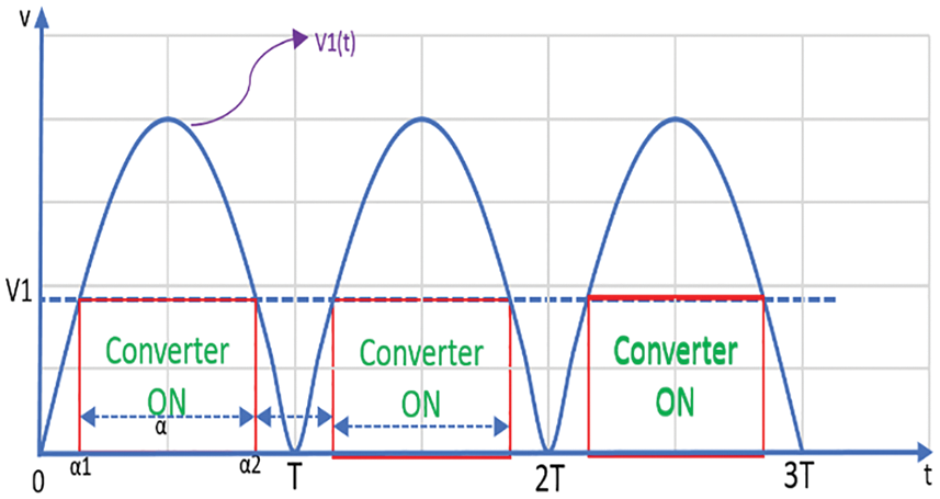
Figure 1: FW rectified signal and converter conduction timings
When the sine wave is measured on both sides of the zero volt, the highest value has to be equal to the amplitude. If there is a DC element besides zero volts, the output waveform is symmetrical at about this point rather than zero [3]. However, similar circumstances have not existed in AC power lines. A wave’s period of time is the amount of time it takes to finish one cycle of the wave, which is significantly represented in Fig. 1. It is used to calculate the frequency of a wave ƒ using the equation T = 1/ƒ.
If the frequency of a signal is 50 Hz, the period has to be 20 ms (1/50) because the input signal follows a sinusoidal function. The waveform V1 (t) in Fig. 1 denotes a full wave rectified signal. The minimum working voltage has to be defined as input voltage threshold to turn on the converter. It is determined by the converter minimum DC operating voltage available in the controller data sheet.
The angle α1 is the converter triggering voltage point. The converter has to turn on above this point at any condition. After the angle α2, the converter has to be switched off.
If we take the difference between α1 and α2, we will get the conduction angle for the converter. The Eq. (5) represents this.
The converter output capacitors provide load current for a few milliseconds even if the input power is unavailable, which is referred as converter’s holding current. The suggested technique employs a load current prediction network, which creates the load current condition for the following cycle prior to the holding current time. As a result, the load state is forecast and the converter acts against the load current variation if necessary. The frequency of this operation is equivalent to the switching frequency of the converter because the power unit supply output ripple frequency matches the switching frequency of the converter. If the load is constant, the waveform has a continuous repeated shape. When the load current suddenly changes, the current gets fluctuated.
Load prediction and output sense circuits are merged into a single circuit. There is no need for an additional output sense circuit if it already exists in the converter. The converter switching operation and Pulse Width Modulation (PWM) control circuits differ but these circuits have to operate in accordance to variations in input voltage and load current. This circuit is implemented using software logic or hardwired logic circuits [4]. If a microcontroller is included in the design, it is recommended that the PWM control has to be done with software logics. The proposed architecture block diagram is depicted in Fig. 2.
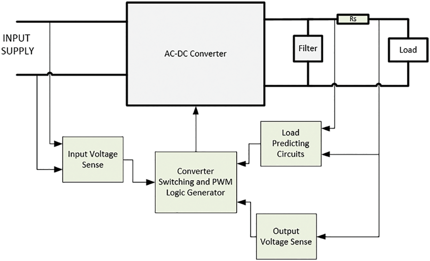
Figure 2: Proposed architecture block diagram
Fig. 3 shows an approximate sketch for load ripple current waveform. There are two cycles for constant load followed by two cycles for an increase in load current.
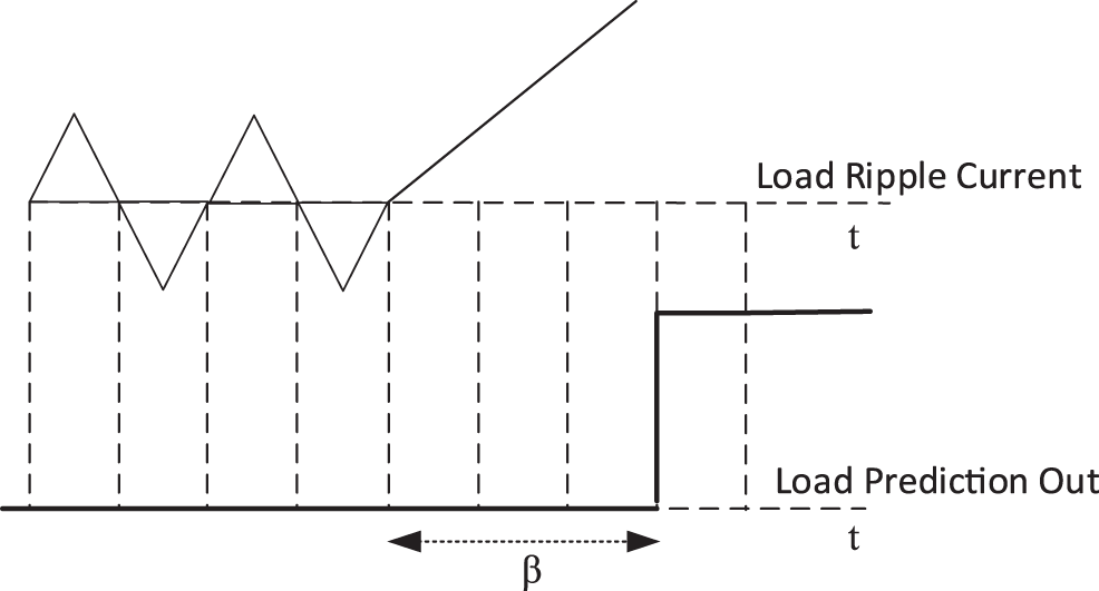
Figure 3: Output ripple current and load prediction
There is a current ramp during the increment time of load current, which has to be determined by the control circuit and control action has to be taken place.
2.2 Control Logic for Load Current Prediction
The load current ripple sense is linked to a current detecting circuit, which generates two output signals like D(t) and C(t), among which C(t) acts as the clock signal for the proceeding section. It is a clock frequency that is synchronous to the converter switching signal. Its zero crossing is defined by the average ripple current value. D(t) is a logic signal that increases as the out loading current increases and decreases as the out loading current decreases. To make a decision on load current change, at least three consecutive D(t) signals have to be observed. The load prediction control logic is clearly depicted in Fig. 4.
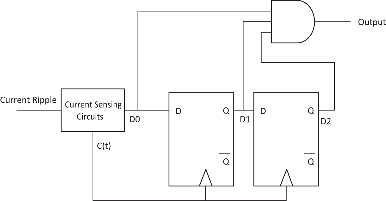
Figure 4: Control logic for load prediction
If the prediction logic signal is getting consecutive high signals, then there is an increase in load current requirement. If the prediction logic signal receives successive high and low signals, the load current remains unchanged. If it is getting low signal sequence, then there is a decrease in load current. C(t) is the clock signal in Fig. 4, D0 is the current state of the current ripple, D1 and D2 are the previous two consecutive states of the current ripple whereas P (output) is the logic output from the current prediction circuit. The circuit contains two logic memory or flip flops that are used to store the previous two values of the current ripple logic outputs. The expression for the output P is given as,
3 Ripple Current Sensing Circuit
Switched-Mode Power Supplies (SMPS) are used to control the input voltage. When building a power supply, the designer considers a high output voltage as an important characteristic because ripple in the design is an important factor [5].
It is derived from the sensing resistor, which is connected in series with the load. This signal is routed to the ripple current detection circuit as depicted in Fig. 5. This circuit is made up of two Operational Amplifiers (OPAMPs), a filter circuit, a peak detector and an average detector. A filter circuit is used to delay the ripple signal. The ripple current waveform’s peak value is detected by the peak detector. The average detector returns the average value of the ripple current waveform. The peak detector output and ripple signal are sent into a single OPAMP circuit, which produces an output for the load prediction logic. When the average detector and ripple signal are linked to various OPAMP circuits, the clock signal for the load prediction logic is produced. The usual operating amplifier’s open-loop system gain AO provides voltage output interpretation. It is expressed as,
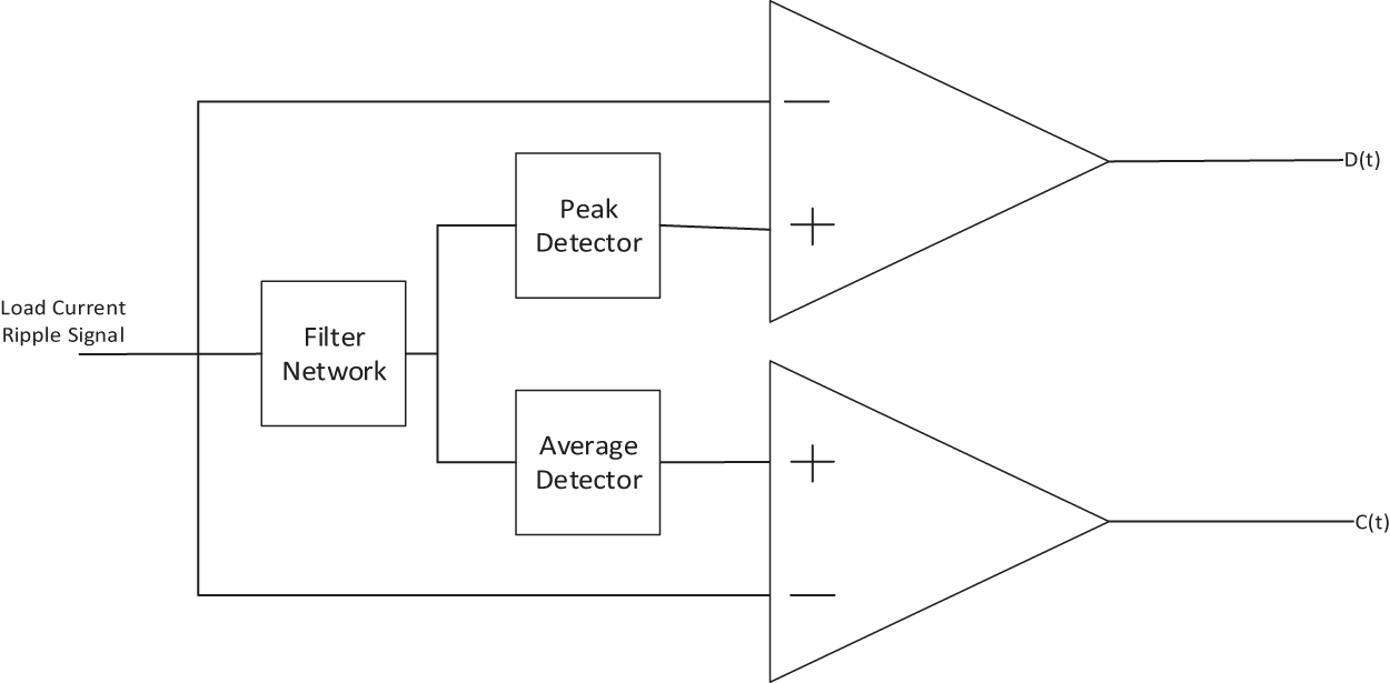
Figure 5: Load current sensing circuit
When the voltage source is slightly lesser than the reference value, the op-output amp returns to its minus saturation level, which allows it to function as a threshold detector. When the input voltage is lesser than the input reference voltage, the op-amp voltage comparator is a circuit that is dependent on both the input voltage and the input reference voltage [6].
The connection of the D(t) signal to the source of the D Flip Flop is shown in Fig. 4, in which D0 is the current input value, and D1 and D2 are the D’s previous two input values (t). By providing a C(t) clock signal, these signals perform logical AND. To change the delay with converter holding time, an extra delay control circuit is necessary, which is accomplished by using the filter network portion. There are two peak detector circuits connected in this load current sensing circuit. It has a major role in this circuit while predicting the load current sensing status. Fig. 6 shows an approximate implementation of the peak detector circuit, which has one operational amplifier, one diode and one capacitor.
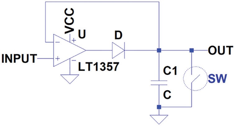
Figure 6: Peak detector circuit
Whenever an input signal comes, the operational amplifier provides an output at the cathode terminal of the diode. The use of operational amplifier is not relevant if the input signal always has higher values. The diode forward biases and it keeps the capacitor charge constant without discharging it back to the operational amplifier. The capacitor needs a slow discharging path, which is not shown in this circuit for the next entry voltage from the input signal.
The value of electronic simulation results depends on how well it predicts physical reality and how quickly it produces results. A mismatch between the simulator and the actual performance sends a product into expensive repetitive debugging cycles [7]. Analog Device LT-Spice is a semiconductor-based electronic circuit simulator computer program. It is related to Simulation Program with Integrated Circuit Emphasis (SPICE) The LT-Spice circuit simulation tool is used here to perform computer simulation and verification of specific architecture.
Fig. 7 depicts a simulation circuit for the input voltage monitoring circuit. The direct current is connected to the rectifier circuit, which converts the DC into rectified DC voltage. Two voltage divider circuit resistors R30 and R31 as well as R28 and R29 connect the sensing circuit directly to the AC supply’s both terminals. The design employs two OP-Amp circuits to monitor the input supply levels by comparing them to a 2.47 V reference voltage.
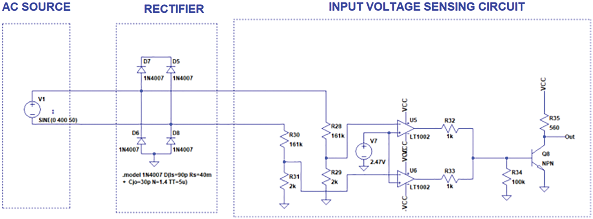
Figure 7: Input voltage monitoring circuit
The input voltage sensing circuit is connected parallel to the AC–DC converter. It works as a supervisory circuit, which controls the AC–DC operation according to the available input supply from the AC source.
The simulated waveforms of the input voltage monitoring circuit are shown in Fig. 8. V[n002] and V[n003] are the input AC source waveforms, which are configured in the simulation tool to 400 V peak voltage and 50 Hz signal. Fig. 8 depicts a full-wave rectified alternating current signal. The signal V [n005] represents U5 output and V [n009] represents the U6 output. In addition, V[out] represents the Q8 transistor collector voltage. V[n002] voltage marked in the graph to show the Vout trigger point, it has changed the state when the input voltage crosses below 200 V in the Op-amp input terminals. Fig. 9 depicts the Vout waveform from the input voltage monitoring circuit, which pulls down the fly back converter MOSFET gate to ground.

Figure 8: Input voltage monitoring waveform
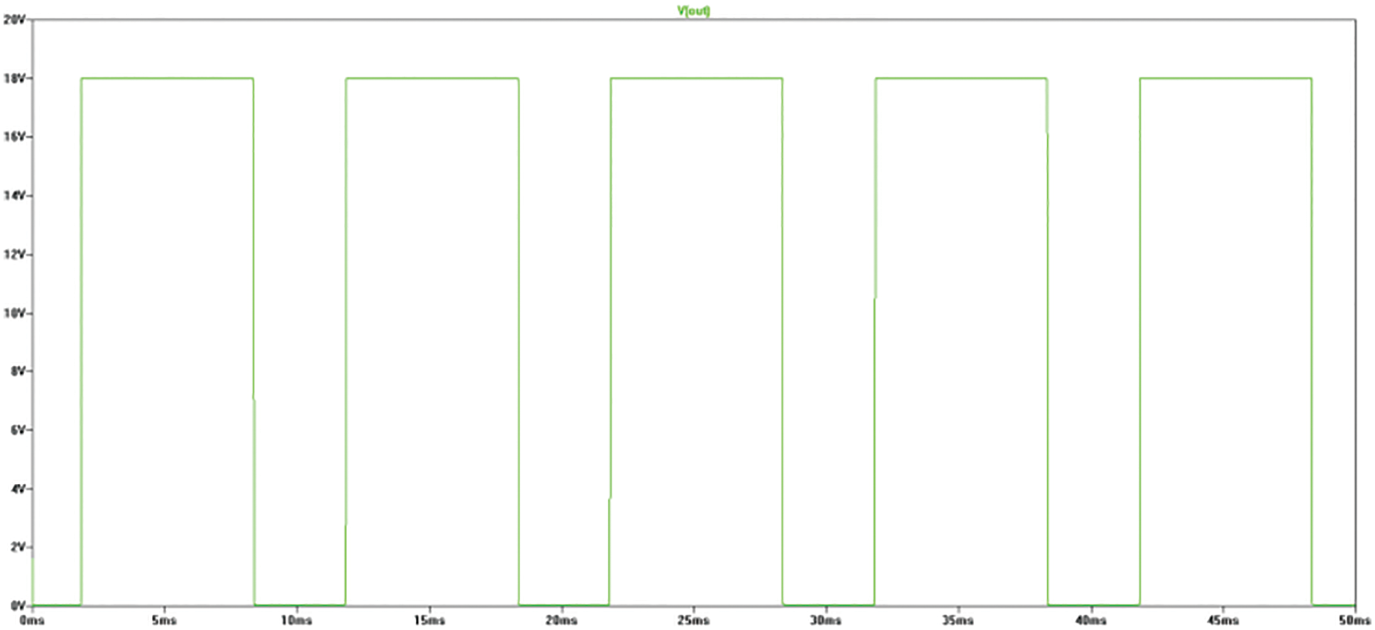
Figure 9: Input voltage monitoring waveform
The triggering angle is computed using Eq. (3).
The designed triggering point is placed at 30° from the incoming sine wave impulses. The input waveform is not switching continuously to the output. Triggering occurs at 30° and ends at 150°. In each half cycle of the full wave rectified outputs, it conducts just 120° out of 180°. As a result, the conduction voltage gets increased to 200 V in each cycle.
The output of the load sense circuit is a square wave. If no current is necessary, the output is a high and low pulsing signal. If additional load current is required, the output constantly remains high. Fig. 10 depicts a circuit that easily find out this logic without the need of any software or a microcontroller.
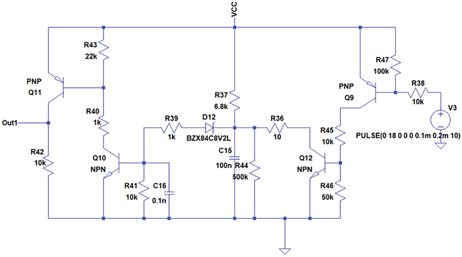
Figure 10: Load prediction circuit
V3 is the signal from the current sense circuit and Out1 is the logic used to determine the load current condition. R38 resistor is used to limit the current to the base of the Q9 transistor and R47 resistor is used to pull up the base of the Q9 to high. In ensures that the Q9 PNP transistor is always turned off if no signal is received from the V3 source. The R45 resistor is used to limit the current flowing through the Q9 transistor and to control the current flowing through the base of the Q12 transistor. The Q12 transistor controls the discharge of the C15 capacitor. When Q12 is turned on, it short circuits the C15 capacitor to ground and allows this capacitor to discharge to ground. R36 resistor is used to limit the discharge current to ground. If R36 value is too low, the capacitor’s life is reduced.
C15 capacitor has a direct path of charging to ground via R37 resistor. When the Q12 transistor is turned off, the capacitor charges to the VCC level. In this circuit, the D12 Zener diode also plays an important role in determining the turn ON time of the out signal. R44 resistor is used to control the self-discharge of the C15 capacitor. When the base junction of Q10 transistor receives enough current to turn on, it turns on Q11 transistor. When there is a pulsating signal from the V3 source, the R41 resistor is used to pull down the Q10 base to ground potential, which ensures that the transistor is turned off. The Zener diode D15 is used here to adjust the Q10 transistor’s base triggering voltage point [8]. The Out1 signal is taken from the Q11 collector terminal and the inverted signal Out1 is connected to the fly back controller’s FB pin. The input and output waveforms of the load prediction circuit are shown in Fig. 11. V(out1) represents the circuit’s output waveform and V(n012) represents the circuit’s input signal. When the V(n012) signal remains high for an extended period of time, the out1 signal goes high. The time constants C15 and R44 play an important role in the design. If the time constant is low, it detects very short high state. If the time constant is high, it detects long high state condition [9]. As the capacitors are being used to hold charge, a mechanism has to be developed to modify the capacitor’s charge state. After nearly 0.5 ms, the out1 signal becomes high, which indicates that the input signal from the V3 source has crossed the designed time of high state. Input remains high until 2 ms and out1 remains high until that time to indicate the status. After 2 ms, V3 signal goes suddenly low, immediately Out1 goes down to indicate that the V3 source is not in high state. The important things need to observe here is that the time to go to low state is very short and going high state has a delay of almost 0.5 ms. This operation continues if the input signal is pulsating.
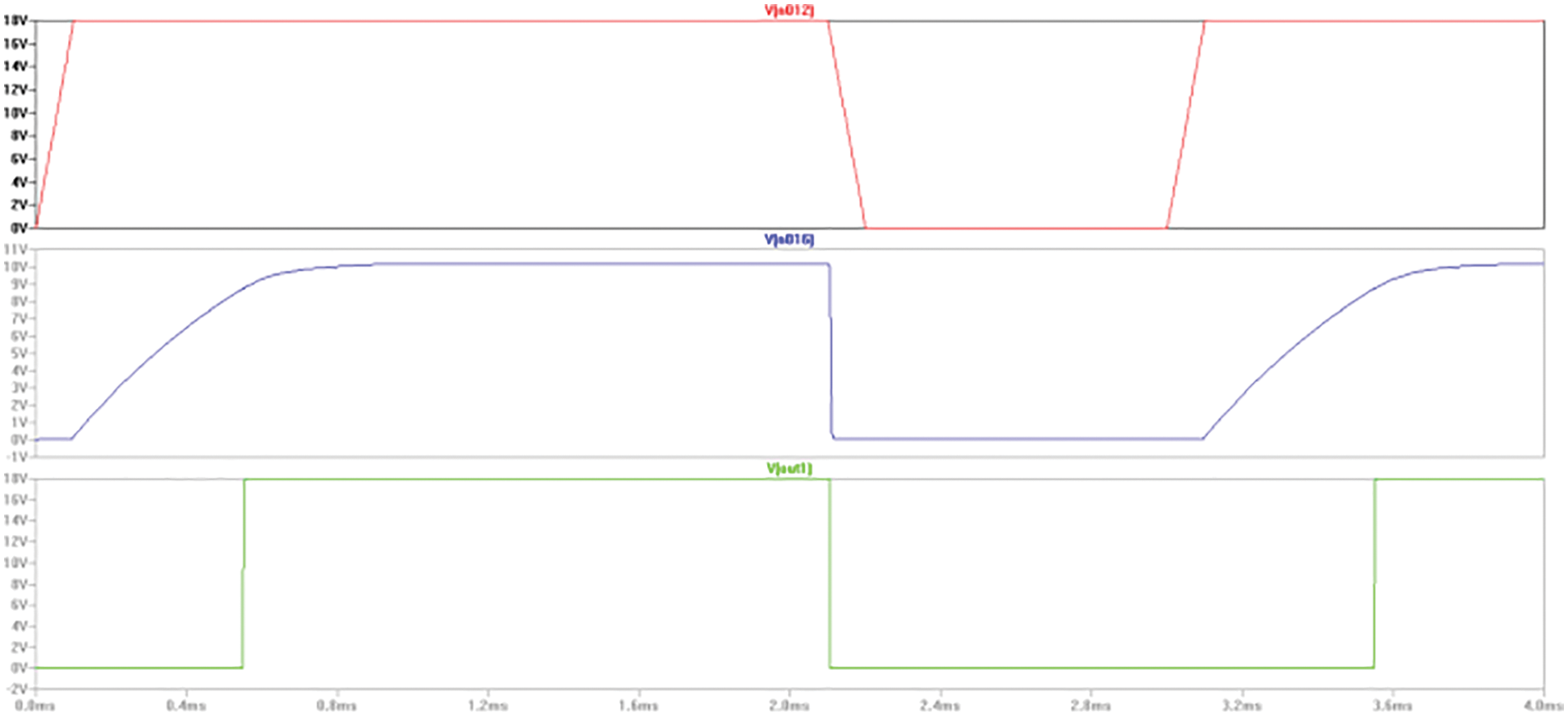
Figure 11: Load Prediction Circuit C15 Waveform
The voltage increase across a capacitor is expressed as,
where Vc(t) is the voltage across the capacitor and V0 is the capacitor’s initial voltage.
Fig. 10 depicts the C15 discharge waveform, which aids in determining the output1 trigger point. V(n012) represents the input waveform, V(n016) represents the voltage across the C15 capacitor and V(out1) represents the output signal. The waveform shows that the C15 voltage is exponentially increasing when it receives a high signal from the input circuit. Once the capacitor voltage crosses the threshold to trigger the D15 diode, it immediately switch the out1 signal ON. It is taking almost 0.5 ms to change the state from Out1 from zero to high state. The discharge tie has to be selected in accordance with the converter’s switching frequency. As the ripple frequency of a converter is always equal to the switching frequency, the time constant has to be greater than the switching frequency. To avoid false switching of the circuit, the time constant has to be greater than three times the switching frequency.
4.3 Frequency Detection Circuit Triggering Point Detection
The load prediction circuit is a frequency detection circuit, which provides a high signal when the input frequency is lower than the set value. Fig. 12 shows an equivalent diagram of the load prediction circuit or frequency detector circuit, in which the capacitor C1 defines the critical role in the frequency calculation. The resistors R1 and R2 support C1 to get charged and discharged according to the input signal. The switch, SW is used to indicate the input frequency signal. When the signal is high, the switch gets closed whereas the switch gets opened when the signal is low. When the Zener diode, VZ crosses its break down voltages, it has to trigger the output. In the calculation, VZ is the breakdown voltage. The resistors R1 and R4 regulate the Zener current. Fig. 12 depicts the equivalent circuit of the OFF condition of Switch. The capacitor charging time is computed by the R1/R2 value.
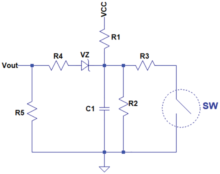
Figure 12: Frequency detector equivalent circuit
The open condition of the switch indicates that the input signal is active. The Zener diode starts conducting only when the voltage across C1 exceeds VZ. As a result, this section is also ignored in this calculation. Across the C1 capacitor, the Thevenin is equivalent.
Thevenin equivalent across the C1 capacitor when the switch is turned off yields this equivalent circuit. When the switch is turned off, the equivalent circuit is shown as in Fig. 13.

Figure 13: Equivalent circuit-switch is OFF
The resistance of R2 >> R1, so
When VZ > VC1, the output is triggered.
If there is any pulse coming more than tH pulse width, the output gets increased. The load current sense output is always in pulse mode with the same frequency as the converter switching frequency. Hence, the output is always in the OFF state.
When the Switch SW is in ON state, the resistor R3 is in parallel with C1 and R2 as illustrated in Fig. 14. The resistance value of R3 is highly lower than R2. As the resistance R1 >> R3, there is no need to consider R1 resistance value while doing C1 discharge calculation.

Figure 14: Equivalent circuit-switch is ON
The maximum voltage come across C1 is VCC. The C1 discharge equation is expressed as,
The resistance of R2 >> R3
The value of tL indicates the maximum time required in the output to transition from a high to a low state. As a thump rule, the tL value has to be less than one-tenth of the tH value. It allows a faster transition from high to low in the output.
The transistor Q10 triggers the output whereas the Zener diode triggers the base. If the required current is not available, the system gets failed at a slightly higher voltage level. Fig. 15 depicts the Zener conduction path in the circuit and the Zener requires a specific current to break down. In this circuit, the base emitter junction of the Q10 transistor is replaced with a diode VBE drop. Hence, the equation to find the current through the Zener is written as,
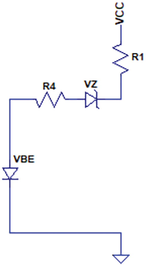
Figure 15: Zener diode conduction path
The LT3798 is an isolated fly back controller that requires no opto-coupler of output voltage feedback for a single output power supply. By continuously regulating the input current using the LT3798 controller, the system achieves a power factor (PF) better than 0.97. The diode current in a flyback converter has a triangular waveform structure with a peak of the maximum secondary winding and a base of the flyback period. The output winding current, Nx, is the primary coil current whereas NPS is the primary to secondary coil ratio [10]. The circuit representation of an AC–DC Converter is evidently illustrated in Fig. 16.
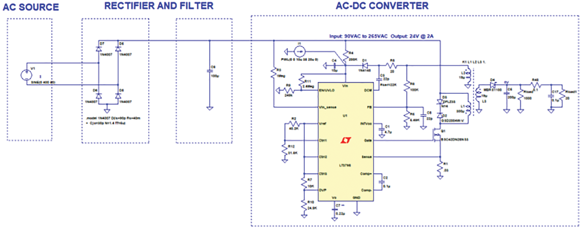
Figure 16: Circuit diagram of an AC–DC converter
During flyback time, the base current is half the secondary coil peak current and zero for the rest of the cycle. The formula is expressed as,
where D denotes the duty cycle represented by the flyback time.
The FB pin voltage division resistors are used to set the output voltage. From the schematic design, the resistors R6 and R5 create a resistor divider [11]. At the FB pin, there is an internal current source that compensates the diode drop. This current source technology is used to adjust the increased voltage requirement caused by the diode loss. The output voltage is calculated as,
where VBG denotes the internal reference voltage, NST denotes the winding ratio between both the secondary and third winding coils, VF denotes the outputting rectifier’s forward dropout and ITC is the inside current of the FB pin. It is preferable to provide time again for the third winding to energize the component if there is a voltage difference between both the turned off and the turn-on conditions of input voltage. The EN/UVLO has picked these two volts [12]. When the pin voltage is less than 1.25 V, this pin sinks almost 10 A of current and sinks nearly 0 A when the pin potential is more than 1.25 V. The UVLO threshold is denoted as,
Consider R5 as a known value and then apply Eq. (19). The resistor values for R6 are calculated by,
The supplied voltage to the flyback converter is 230 V AC, which has a maximum voltage of 400 V waveform in a single ended measurement. Fig. 17 shows the AC–DC converter waveform. The first waveform represents the input supply, which has measured variations between node 3 and node 6 in the circuit. V(n001) represents the rectified wave after capacitor filtering. The capacitor selected here is 100 uF [13].
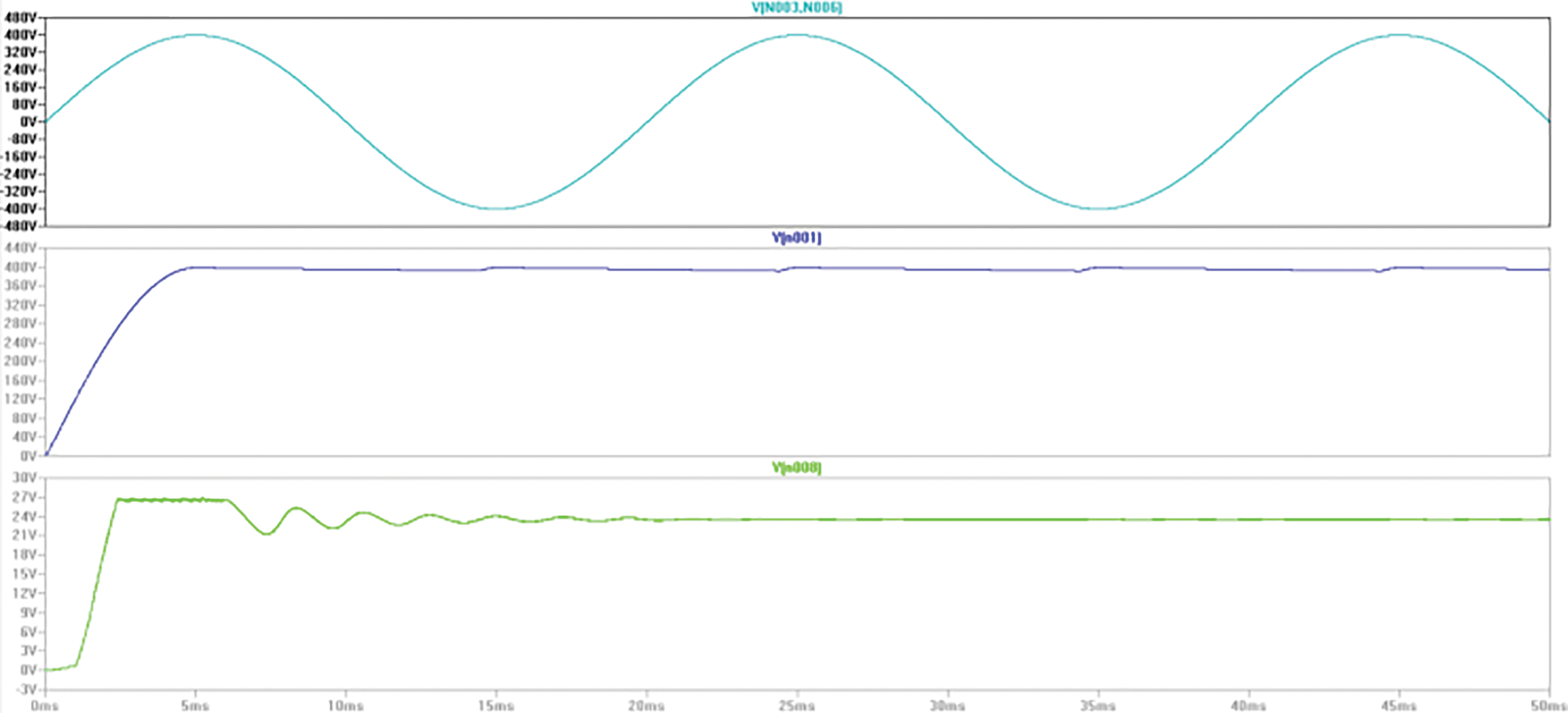
Figure 17: AC–DC converter waveforms
The designed output voltage is 24 V and the output voltage waveform is represented as V(n008). When the output voltage reaches a steady state, it becomes more stable. Constant power supply ripple is typically measured at twice the normal line frequency. The proposed method has little higher ripple voltage compared to the existing method. Fig. 18 depicts the current flowing through the R1 resistor, which is connected from the source to the ground of a flyback MOSFET [14]. It functions similarly to the gate pulse applied to the MOSFET.

Figure 18: AC–DC converter input voltage and gate PWM signal
4.5 Converter Performance After Proposal Implementation
The proposed method needs few additional monitoring circuits to decide the converter turn ON and OFF conditions. Fig. 19 depicts the proposed system, in which an AC source is connected to a rectifier circuit as well as an input voltage monitoring circuit whereas a voltage divider circuit is placed before the voltage monitoring circuit to prevent the presence of high voltage on the monitoring circuit. The capacitor C6 used for filtering the ripples from the rectified DC and its value used here is only 0.47 uF. The major advantage is that the value of this capacitor is reduced to 0.47 from 100 uF.

Figure 19: Proposed AC–DC converter
Voltage across R48 resistor is linked to the input of an electrical energy follower circuit, which gives an output equivalent to the ripple current through the load. An op amp-based comparator as opposed to an op amp compares two inputs and delivers the result of the evaluation
The input power signal is represented by the V(N003, N006) waveform and the flyback gate pulses are represented by the V(n20) signal. V(n008) represents the output voltage values. The primary functions of a power supply are to convert an input voltage to a designed output voltage as represented in Fig. 20. The accuracy of this voltage and the amount of voltage variation under different conditions depends on the output regulation. The input voltage level has to be kept within a certain range [15]. Even though, this variation exceeds the designed limits, it causes the problems in many sensitive equipment because it causes deviation in the output voltage. V(n008) represents the output voltage of the converter and the output is loaded with 20 Ohm resistor. The voltage has a small variation from the above waveforms but is okay for this specific application.

Figure 20: Shows the gate pulses and the output voltage waveform
The primary application for this proposed solution is Brushless DC (BLDC) based ceiling fans. A BLDC motor is an electronically commutated motor that is powered by a DC electric power supply. Current vs. torque and voltage vs. rpm have linear correlations in BLDC drive systems. This work focuses on the actual implementation of the BLDC motor as a ceiling fan using the technique proposed in [16]. Ceiling fans use a lot of power from the power source to control the RPM with the help of capacitor or resistor-based controllers. Input voltage-controlled speed control method uses for ceiling fans, which causes abnormal problems due to voltage changes in the mains [17]. Power considers degradation is caused by an AC motor. The sharp edge decides the air flow and speed of fan and fails to change because of any other variables. BLDC based ceiling fans provides better efficiency and constant speed control when compares with existing conventional ceiling fans.
The converter operates in the suggested approach whenever the voltage level exceeds the specified intended value, which in this case is 200 V. As a result, the converter only activates when the voltage level is more than 200 V. Fig. 21 shows the simulated waveform.

Figure 21: Gate pulses and input voltage
4.6 Proposed System with BLDC Motor Load
Power tools are used in a variety of household applications like gridding, fastener driving, drilling, gardening tools, cutting and polishing. Electric motors are commonly used in power tools. Machine tools seem to be either battery-powered or electrically operated (corded or cordless). The input power gives the DC or AC engines in wired power tools. Battery-powered tools employ DC motors to run on battery power [18]. BLDC motors require minimal maintenance and more productive with long life span and lower noise and the circuit representing the BLDC implementation is highlighted in Fig. 22 and the electrical Waveforms in BLDC is portrayed in Fig. 23.
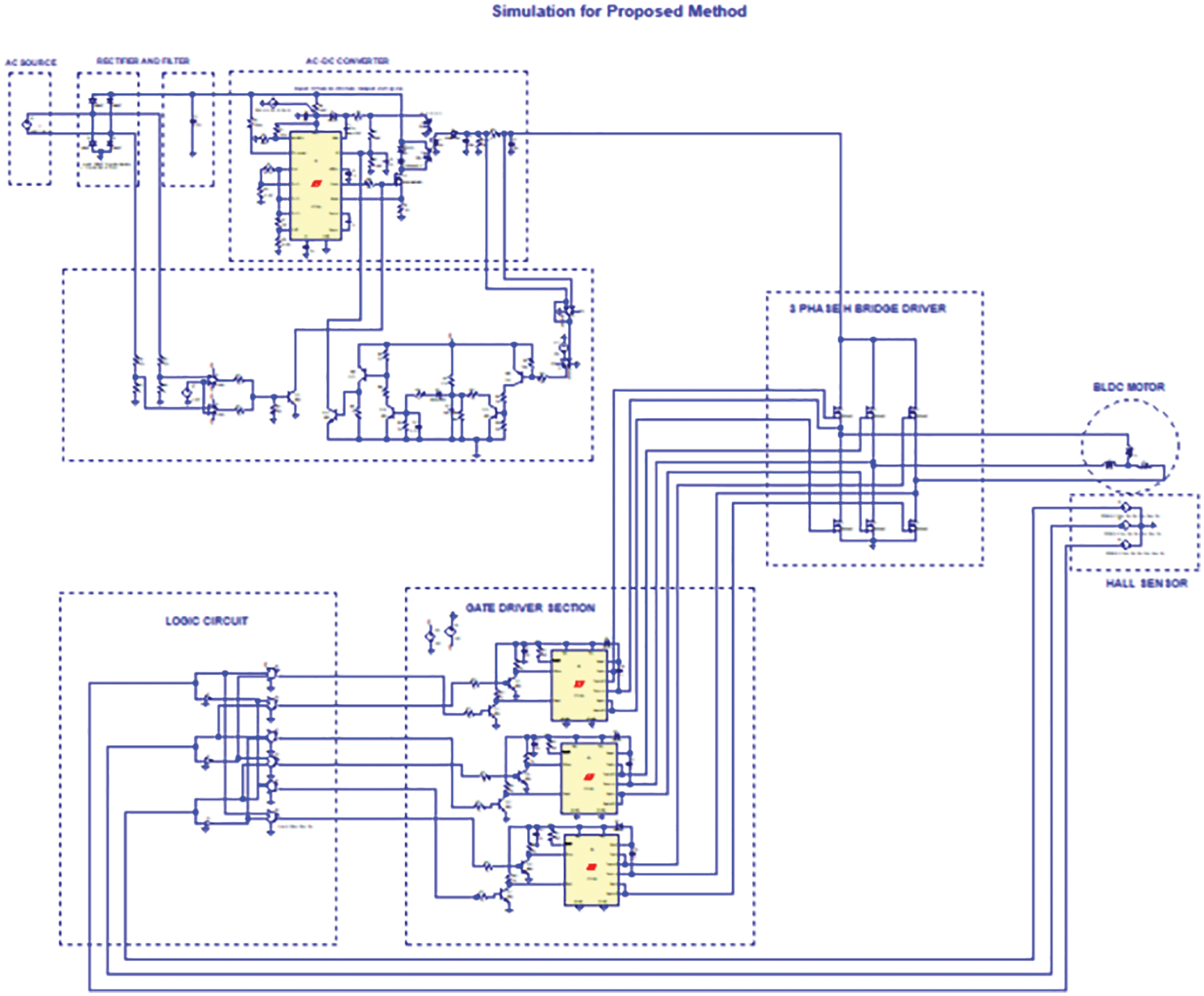
Figure 22: Proposed circuit implementation with BLDC

Figure 23: Electrical waveforms in BLDC motor
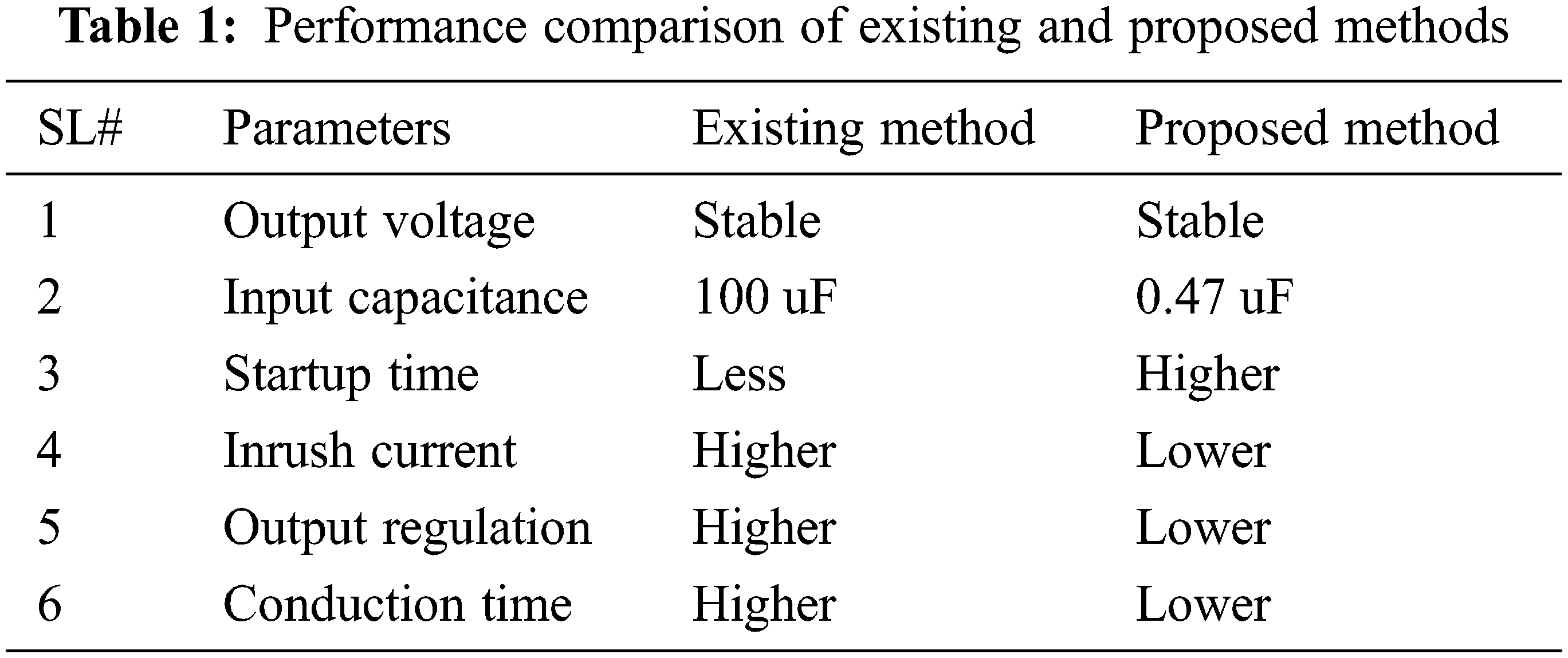
Permanent magnet engines are classified into two types as BLDC motors and Permanent Magnet Synchronous Motors (PMSMs) based on the Back-EMF (BEMF). Both BLDC and PMSM motors use permanent magnets on the rotor but have different BEMF patterns and flux distribution patterns. The BEMF variation in the stator of a BLDC motor is trapezoidal whereas the BEMF variation in the stator of a PMSM motor is sinusoidal. A good and efficient control technique has to be used to get high performance [19]. The trapezoid BEMF or BLDC motor’s stator has to have an ampere conductor or current distribution. The commutation interval for a three-phase winding is 60° electrical. The pairing of direct current and a trapezoidal BEMF allows the generation of a fixed torque [20]. As the current is created instantly in a motor stage in practice, each 60-degree phase commutation contains a torque ripple. The comparative analysis of the proposed approach with other conventional approaches is significantly highlighted in Tab. 1.
The output voltage of a converter has to be stable to the designed voltage because it is a basic requirement for all switch mode converters. The output of switch mode converters has ripples and the quality of the converter is defined by the amount of ripples in the output. The proposed converter is applicable for fixed and constant load applications. The application voltage is not critical in this case and a wider input voltage tolerance range is also acceptable for this type of application. Even if the proposed concept has little variation in the output voltage as in Fig. 24, it is acceptable [21].

Figure 24: Output voltage waveform of proposed method
Designing a converter for applications that require a low output noise level results in a delayed startup due to an excessive output inrush current. Output inrush current is caused by improper design and its effect on output filters, soft start time, switching frequency or output capacitance. Industrial applications that draw current from a 4–20-mA current loop or energy harvesting has to store the required energy at the input capacitance before turning on the converter [22]. In the absence of sufficient power, the converter takes in-rush current and cause the converter to reset. In a worst-case, the system never starts at all.
Though the converter output voltage has little ripples, it meets the specific application, which is planned to implement this method. Fig. 21 depicts the proposed method’s output voltage waveform with the output ripple ranging from 18.88 to 18.52 V. The ripple voltage is 0.32 V, which is lesser than 0.5 percent of the output voltage and is suitable for the application.
AC–DC converters are used in power electronics equipment such as commercial, medical, military, and telecommunications applications. The use of high value and high voltage rated DC link capacitors reduces the power density of the converter and limits the product reliability. This paper introduced a novel approach to this problem and examined its viability. There is a feasibility to reduce DC link capacitance value for AC–DC converters to reduce the input ripple current. Simulations are done for each section and its results are analyzed to get more clarity before preparing an actual proto. Control logic circuit requires further analysis and needs to be prototyped for testing. There are some disadvantages such as low regulation, more ripple voltage, etc. but there are some specific applications where this parameter is not so important. The recommendation is to look for and implement this type of application. There are numerous future applications for this paper. For example, it is possible to use this method in the aerospace industry and specific commercial products.
Funding Statement: The authors received no specific funding for this study.
Conflicts of Interest: The authors declare that they have no conflicts of interest to report regarding the present study.
References
1. T. Agarwal, “A review and comparative study on single-phase AC–DC converters for their high frequency application,” in Int. Conf. on Communication & Computational Technologies by RIET, Jaipur, IJCRT.ORG, 2017. [Google Scholar]
2. R. Kalpana, G. Bhuvaneswari, B. Singh and P. S. Prakash, “Design and implementation of high frequency isolated AC–DC converter for switched mode power supplies,” in Eighteenth National Power Systems Conf. (NPSC), Guwahati, India, IEEE, pp. 1–6, 2014. [Google Scholar]
3. B. S. Grewal, Higher Engineering Mathematics, 44th ed, KHANA Publications, New Delhi, 2018. [Google Scholar]
4. S. Funabiki, “A single-phase PWM controlled AC to DC converter based on control of unity displacement power factor,” Seattle, WA, USA, Okayama University, IEEE, pp. 1012–1013, 1990. [Google Scholar]
5. S. P. Singh, “Output ripple voltage for buck switching regulator,” Application Report, (SLVA630ATexas Instruments, 2014. [Google Scholar]
6. M. R. Rakesh, “Design and implementation of window comparator circuit using operational amplifier,” International Journal for Innovative Research in Multidisciplinary Field, vol. 5, no. 8, pp. 6–8, 2019. [Google Scholar]
7. M. Engelhardt, “SPICE differentiation,” LT Journal of Analog Innovation, vol. 24, no. 4, pp. 10–16, 2010. [Google Scholar]
8. A. C. Maxeine, “Analysis and measur analysis and measurement of a Z ement of a zener diod voltage-reference,” Masters Theses, 3492, 1972. [Google Scholar]
9. L. Vandenberghe, S. Boyd and A. E. Gamal, “Optimizing dominant time constant in Rc circuits,” IEEE Transactions on Computer-Aided Design of Integrated Circuits and Systems, vol. 17, no. 2, pp. 110–125, 1998. [Google Scholar]
10. Onsemi, “Programmable precision references TL431,” Semiconductor Components Industries, LLC, 2021. [Google Scholar]
11. Linear Technology, “Isolated no opto-coupler flyback controller with active PFC,” Linear Technology Corporation 1630 Mccarthy Blvd., Milpitas, CA 95035–7417, lt 1212 Rev A, USA, 2012. [Google Scholar]
12. B. K. Nishanth, “Multiple output fly back converter with primary side current mode control for defence applications,” in Int. Conf. on Smart Grids, Power and Advanced Control Engineering (ICSPACE), Bangalore, India, IEEE, pp. 137–142, 2017. [Google Scholar]
13. S. Kunkolkar and V. N. Shet, “Flyback converter design and simulation,” International Journal of Advanced Research in Electrical, Electronics and Instrumentation Engineering, vol. 6, no. 5, pp. 4077–4087, 2017. [Google Scholar]
14. R. M. Arreola, D. S. Perez, M. P. Silva, H. H. D. Leon, J. A. A. Tapia et al., “Analysis of a DC–DC flyback converter variant for thermoelectric generators with partial energy processing,” MDPI, Electronics, vol. 10, no. 5, pp. 1–16, 2021. [Google Scholar]
15. J. Bryant, “Using Op amps as comparators,” Analog Devices, vol. 849, pp. 1–8, 2011. [Google Scholar]
16. P. C. Sahid., “Energy efficient ceiling fan using BLDC motor,” International Journal of Engineering Research & Technology (IJERT), vol. 4, no. 4, pp. 460–464, 2015. [Google Scholar]
17. A. D. Marvaniya, “Energy conservation in ceiling fan using BLDC motor,” International Journal of Advance Engineering and Research Development, vol. 4, no. 7, pp. 197–199, 2017. [Google Scholar]
18. V. V. Nijil, “Design of wide range input BLDC motor drive based on trapezoidal control,” IJARSE, vol. 7, no. 1, pp. 77–90, 2018. [Google Scholar]
19. Y. N. Kumar, “Speed control of BLDC motor drive by using PID controllers,” Journal of Engineering Research and Applications, vol. 4, no. 4, pp. 37–41, 2014. [Google Scholar]
20. M. Azadi, “Speed control of an eleven-phase brushless DC motor,” International Journal of Information and Electronics Engineering, vol. 3, no. 4, pp. 374, 2013. [Google Scholar]
21. P. Shenoy, “Common mistakes in DC/DC converters and how to fix them,” Texas Instruments Power Supply Design Seminar SEM2300, TI Literature Number: SLUP384, pp. 1–16, 2018. [Google Scholar]
22. C. Glaser, “Achieving a clean startup by using a DC–DC converter with a precise enable-pin threshold,” Analog Design Journal, ADJ 4Q, pp. 1–5, 2017. [Google Scholar]
Cite This Article
 Copyright © 2023 The Author(s). Published by Tech Science Press.
This work is licensed under a Creative Commons Attribution 4.0 International License , which permits unrestricted use, distribution, and reproduction in any medium, provided the original work is properly cited.
 Downloads
 Citation Tools