DOI:10.32604/iasc.2023.025422
| Intelligent Automation & Soft Computing DOI:10.32604/iasc.2023.025422 | |
| Article |
Analysis of Efficient 32 Bit Adder Using Tree Grafting Technique
1KIT-Kalaignarkarunanidhi Institute of Technology, Coimbatore, 641402, Tamilnadu, India
2Sri Ramakrishna Engineering College, Coimbatore, 641022, Tamilnadu, India
*Corresponding Author: R. Gowrishankar. Email: gowrishankarrphd@gmail.com
Received: 23 November 2021; Accepted: 24 February 2022
Abstract: Adder with high efficiency and accuracy is the major requirement for electronic circuit design. Here the optical logic gate based adder circuit is designed for better performance analysis of optical input signals varied with the wavelength. Efficiency of the adder can be improved by increasing the speed of operation, reducing the complexity and power consumption. To maintain the high efficiency with accuracy, a new combination of adder has been proposed and tested in this work. A new adder by combining the logics of Brent Kung, Sklansky and Kogge Stone adders by Tree Grafting Technique (BSKTGT) has been tested along with individual Brent Kung, Sklansky, Kogge Stone, Knowles, Han Carlson and Ladner Fischer adders. All the existing and proposed adders have been designed and tested for efficiency with the help of Cadence platform with 45 nm technology. Efficiency in terms of Size reduction, Power reduction, Power Delay Product (PDP) and accuracy in adding 8 bit, 16 bit and 32 bit values had been tested for all the adders and found that the 32 bit BSKTGT adder performed well in all aspects and have produced better efficiency with the power consumption of 52.512426 μW with 3.16% of power saving over Brent Kung adder, utilised an area of 631.191 with 8.55% reduction over Kogge Stone Adder, has the cell count of 132 which is 10.61% reduction over Brent Kung Adder and PDP value of 122.6695 J, which is 0.46% less than that of the Han Carlson Adder.
Keywords: Design automation; computer integrated manufacturing; autonomous control; communication engineering
Advanced cutting-edge technologies focus has shifted to the optical domain because of its faster rate and lack of electromagnetic interference. Networks of optical splitters, switches, circulators, and many more require the ability to switch at extremely high speeds. Because of the need for electro-optic conversions, the performance of optical networks has been hampered by the employment of virtual gates. That is why photonic networks will benefit from optical signal processing and computing technologies by forcing logic gates to operate exclusively in optical mode. To increase an all-optical network, optical gadgets are the simple requirement. In case of optical gadgets, the signals stay within the photonic model, thereby putting off the digital bottleneck. Consequently, the speed of the gadget can reach up to tera hertz (THz). Therefore, the work prefers to design the optical logic gate-based adder circuit. Adders are the important elements in the application of filters and arithmetic and logic unit (ALU) of processors and computers. Further, adders play a major role in computers for calculation of addresses and other operators like program counter for processing. Initially processors processed a smaller number of bits for all kind of applications. The extraordinary growth in technology forces the designers to go for multiple numbers of bits processing especially in high level applications of optical communication. Hence, adders for multiple bit processing are an important requirement for any circuit which uses it. And for adding multiple numbers of bits, ripple carry adder, carry look ahead adder, carry select adder, carry skip adder, carry save adder and parallel prefix adder with high speed operation is used by the designers. Less area utilisation, faster computation or less delay, minimum fanout or less complexity and low power consumption are the important parameters to be noted for a better adder. Parallel prefix adder with minimum complexity, minimum delay and power consumption is the most needed parameters to be considered for the effective design of high speed circuits.
From the detailed study on the six important parallel prefix adders that had been designed and tested earlier for addition applications, it is observed that, reduction in the time consumption has been successfully tested form the implementation of Sklansky Adder (SA) [1], Kogge Stone Adder (KSA) had been implemented with less fanout and complexity [2], Ladner Fischer Adder (LFA) had been tested successfully for faster computation [3], Simple design with less chip area had been studied from Brent Kung Adder (BKA) implementation [4], Han Carlson Adder (HCA) had been designed with less complexity [5] and Knowles Adder (KA) had been designed and tested for minimum fanout [6]. Parallel prefix carry tree architectures for different adders had been tested and found satisfactory results [7]. Complementary metal oxide semiconductor (CMOS) based adders with power reduction had been tested in [8]. Design of FIR filter by using parallel prefix adder with delay and power reduction had been discussed in [9]. Gate diffusion input (GDI) and CMOS techniques had been tested and compared for size reduction [10]. Modification in the generate term is done in the ling adder for complexity reduction and power reduction of 14.78% when comparing to the actual 32-bit ling adder. Many parallel prefix adders had been discussed for power, delay and area reduction and found that the Kogge Stone adder performed well. Parallel prefix adders had been discussed and found that the Kogge Stone adder had consumed less power with less delay, Brent Kung adder produced moderate amount of power delay reduction with complexity and the Ladner Fischer adder had less complexity with moderate power delay reduction. Hybrid optical reversible logic gate is designed and tested for its efficiency and peres gate performance has been tested in [11]. Optical double-controlled logic circuits have reduced the circuit complexity and power consumption. The mathematically modelled version is visible and features accurate cascading and compactness. Complex common-sense circuits, such as the 16-Boolean common-sense unit, Gray-to-Binary-to-Grey code conversion, and pass-bar network architecture, have also been proposed in this investigation. Reversibility is another feature of the circuits. Method discussed in [12] dealt about the design of a non-linear circuit that uses an optical amplifier and a mode-lock amplifier as a probe for the statistics. When using pass gain modulation, a non-linearity in the semiconductor optical amplifier is introduced. Statistics on peak signal modulation of carrier density in a semiconductor optical amplifier are referred to as cross gain modulation. Additionally, the advantage of variation indentation is that it reverses the probe signal after travelling through the amplifier. Section modulation is converted into depth modulation using an interferometer arrangement. A method in [13] demonstrated XOR gates, two AND gates, and one OR gate were used to create an all-optical binary full adder. An optical amplifier-based Mach-Zehnder interferometer (MZI) is used to discover the XOR gate. Semiconductor amplifier nonlinear homes are the sole source of the AND and OR gates. Input data streams and a bringing-bit from the preceding less-sizable-bit order position are used to drive the suggested system forward. Since optical processing has the potential to overcome intrinsic semiconductor delays and considerable heat generation, it has significantly spurred current efforts to overcome these fundamental performance limits. Photonic devices, which use photons as data carriers, are capable of high speed and capacity, and low power loss [14]. The development of an all-optical common-sense era is needed for a wide range of all-optical network services, including high-speed all-optical packet routing and optical encryption [15].
From the detailed survey, it is clear that, all the existing adders are efficient in any one or two aspects and there is no adder available to perform well in all the three important aspects, that is, power reduction, area reduction and delay reduction. And the desperate need of optical logic gate based adder for optical communication related applications. If any single adder logic or modified single adder logic or combination of any two or three logics to form new adder logic can perform the above said aspects and to produce the accurate results, then it can be further used to design important electronic circuits like multipliers, filters and arithmetic units.
Accuracy is the most important factor to be considered while study, design and examine any adder to be utilised in such electronic circuits. Improvement in the speed of operation, power consumption and the size reduction are the main factors to be considered while looking for the better accuracy. Parallel prefix adders are the one satisfying the above factors. But they are not able to satisfy the complexity issues while they are handling more number of input bits.
To overcome the complexity issues and to retain the higher accuracy, new adders are required. One such adder is the combination of logics of Brent Kung, Sklansky and Kogge Stone (BSK). This new combination has a structure which handles more input bits with less complexity. To achieve the above requirement, the structure has been modelled with tree grafting technique. That is, first two stages are formed by grafting the logic of Brent Kung adder with Sklansky adder and the latter stage is formed by grafting the logic of Kogge Stone adder to the initial stages and named as BSKTGT Adder (BSKTGTA).
After the detailed survey about the structures and efficiency of the existing adders, the new adder has been proposed by combining the structures of the three important and efficient adders. This new combination utilises grey and black cells in an effective way to reduce the complexity.
Optical logic gate-based circuit permits direct parallel switch from an optical processor or storage detail to a widespread electronic gadget. The optical enter beams can be viewed as control indicators or as logical inputs that growth the gadget complexity and permit direct interplay of the digital common-sense circuits with the optical beam states. To support the optical based communication system module design, the proposed adder design is very much needed. Design of any adder consists of three basic processing stages. They are pre-processing: first stage of an adder and it consists of two sub stages named propagate and generate, carry network: the second stage of an adder and it consists of carry propagation and generation and post-processing: the third stage of an adder and it consists of XOR gates for producing the results sum and carry. This processing stage has been increased further for handling a greater number of input bits as per the new design requirements of any adder. That is, the number of stages will increase for increase in input bits. Here, this proposed method utilises the same three stages with a special capability of handling any number of input bits only by three stages. The processing has been described with eight equations as follows.
Pre–Processing Stage:
The generate bit is
and the propagate bit is
from Eqs. (1) and (2), ai–is the ith first input bit and bi–is the ith second input bit.
Carry Network:
Grey cell is
from Eq. (3), gi−1–is the previous generate bit and gcgj–jth is the gray cell generate bit.
and for black cell is
from Eq. (4), bcgj–is the jth black cell generate bit.
from Eq. (5), bcpj–is the jth black cell propagate bit.
Post–Processing Stage:
From Eq. (6) the sum output is equal to propagate output
From (7), sumi–is the ith sum bit and ci−1–is the last stage of generate bit in grey cell and black cell and for carry,
where, bcgj–last jth black cell generate bit.
The stages of proposed adder have been constructed by considering the above equations. And the process flow is shown in Fig. 1.
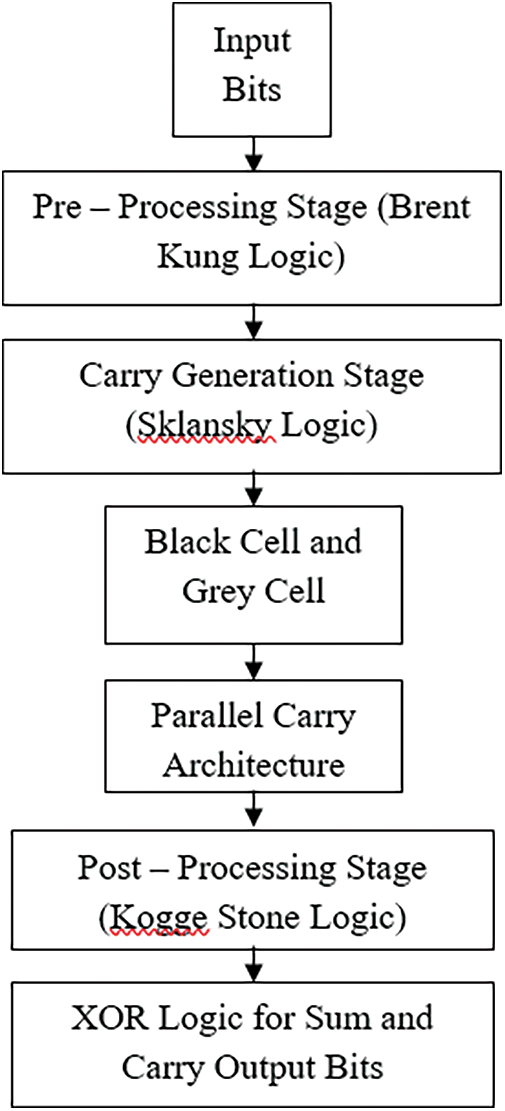
Figure 1: Process flow diagram of proposed BSKTGT Adder
The first stage has been modelled with Sklansky adder and it is almost similar to that of Brent Kung adder’s first stage. The second stage functions with the logic of Kogge Stone adder with the routing logic similar to that of Sklansky adder. And the final stage functions with the Kogge Stone logic alone. First two stages are supported by Sklansky logic even though they are physically Brent Kung and Kogge Stone respectively. This combination along with Kogge Stone logic in the final stage provides a new combination with new structure and named as BSKTGTA. This new combination of adder has only three stages for any number of bits. This is one of the main advantages of proposed this BSKTGTA and it can be utilised for larger number of input handling applications. This work includes the design and comparison of 8 bit, 16 bit and 32 bit adders. Structure of 4 bit BSKTGT adder is given in Fig. 2.
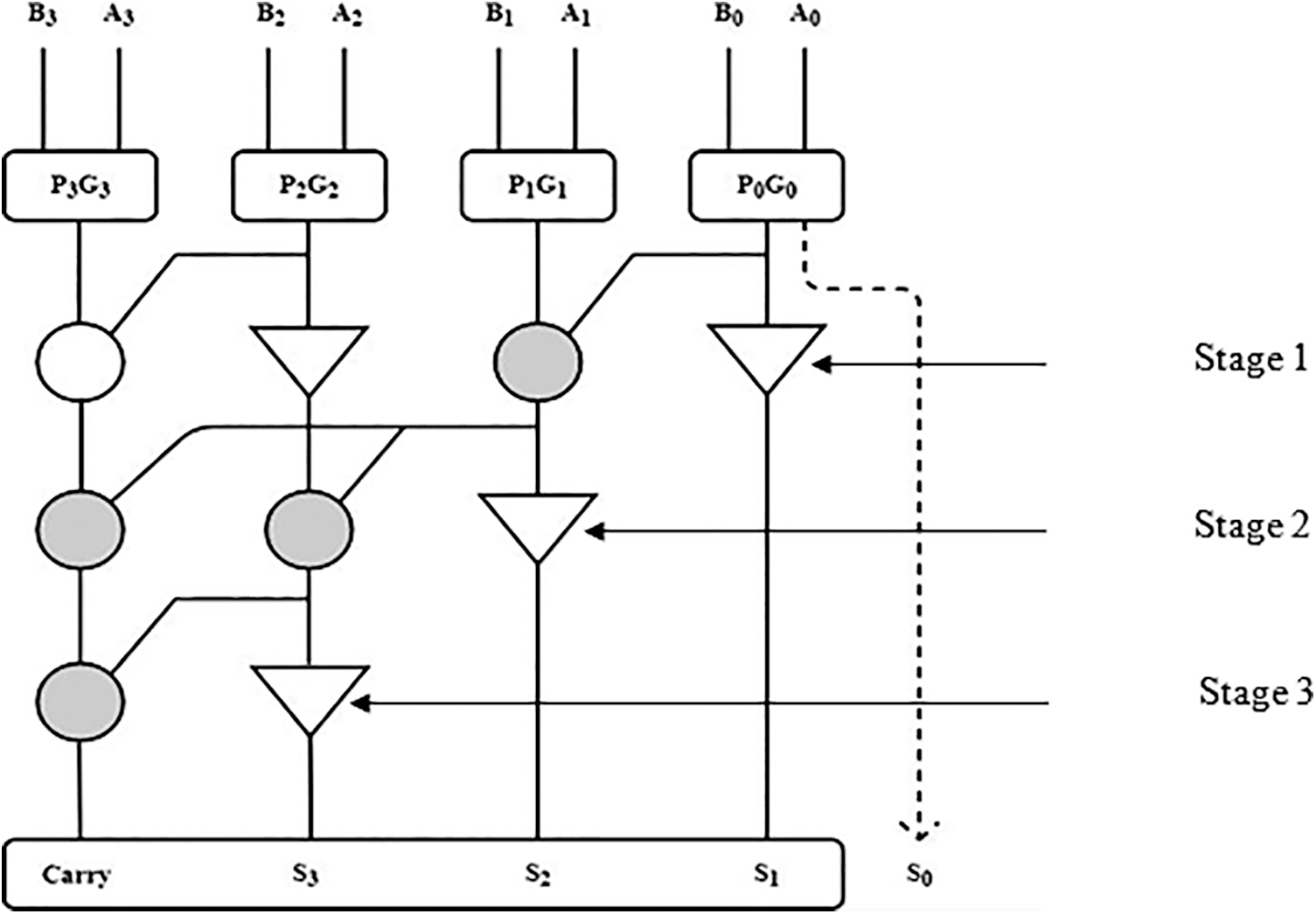
Figure 2: Structure of 4 Bit BSKTGT Adder
With the help of four bit logic, the structure of proposed 32 bit BSKTGT adder has been designed and given in Fig. 3. From the outputs of the proposed complete adder circuit, retrieving the input bits is very easy and this makes the scheme novel one. Thus, the proposed 32-bit adder will be helpful for designing numerous sorts of optical processors with less power dissipation.
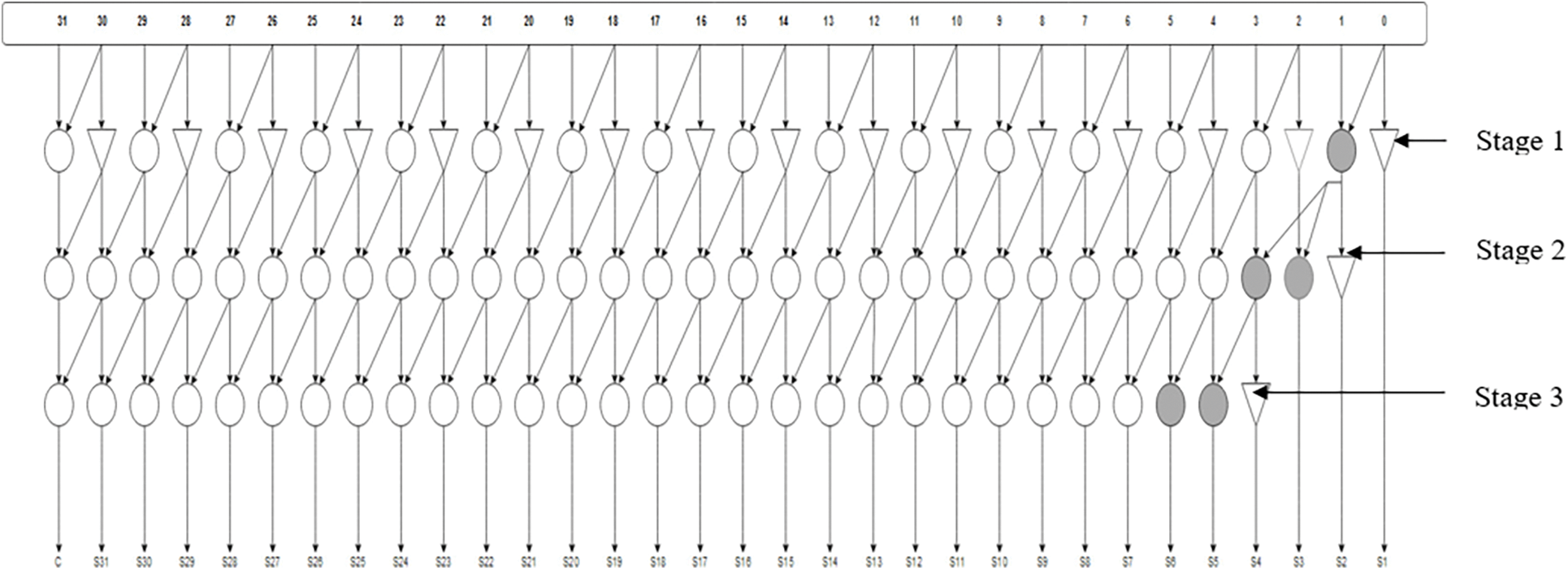
Figure 3: Structure of 32 Bit BSKTGT Adder
The complete adder is a logic device that performs the addition of three binary digits. In a cascade of adders, it adds eight, sixteen, or 32-bit binary values in a sequential manner. Stages A, B, and C of a one-bit full adder add three one-bit values together with operands A and B and a-bit carried over from the previous much less significant degree. From Fig. 3, we have stages one, two and three of proposed 32-bit BSKTGT Adder with-bit 01 (S1) to-bit 31 (S31) consists of black cell and buffer for SUM output bits and the last-bit is grey cell (C) for CARRY output bit. The first SUM output-bit S0 comes along with the SUM output-bit S1 as shown in Fig. 2.
From Tab. 1 and Fig. 4, it is clear that, the Kogge Stone, Knowles and Sklansky adders required 05 stages, Han Carlson and Ladner Fischer adders required 06 stages, Brent Kung adder requires 08 stages and the BSKTGT adder requires only three stages for processing 32 bit input. Input and output stages are excluded for total cell count calculation and stages required only for processing been considered for total cell count calculation.
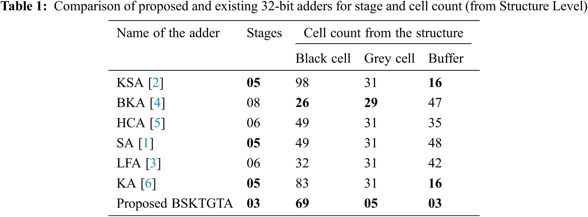
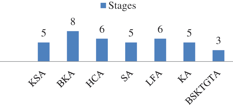
Figure 4: Stage analysis of adders
From Tab. 1 and Fig. 5, it is clear that, the Brent Kung adder has the less number of black cell with 08 stages and the proposed BSKTGT adder has less number of grey cell and buffer with only three stages. And the other adders have more number of stages as well as cells. The tree grafting structure made the total cell count is less for the proposed BSKTGT adder in the structure level.
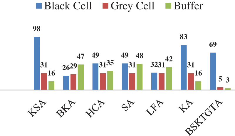
Figure 5: Analysis of cell count form the structure of adders
To verify the operation, two 32 bit data (FFFFFFFF and AAAAAAAA) have been given as input for all the adders discussed in this work. And the result shows that all the adders have performed the same addition operation with the resulted Sum: AAAAAAA9 and Carry: 1. The simulated waveform of proposed BSKTGT adder is given in Fig. 6 and the RTL schematic diagram is given in Fig. 7.
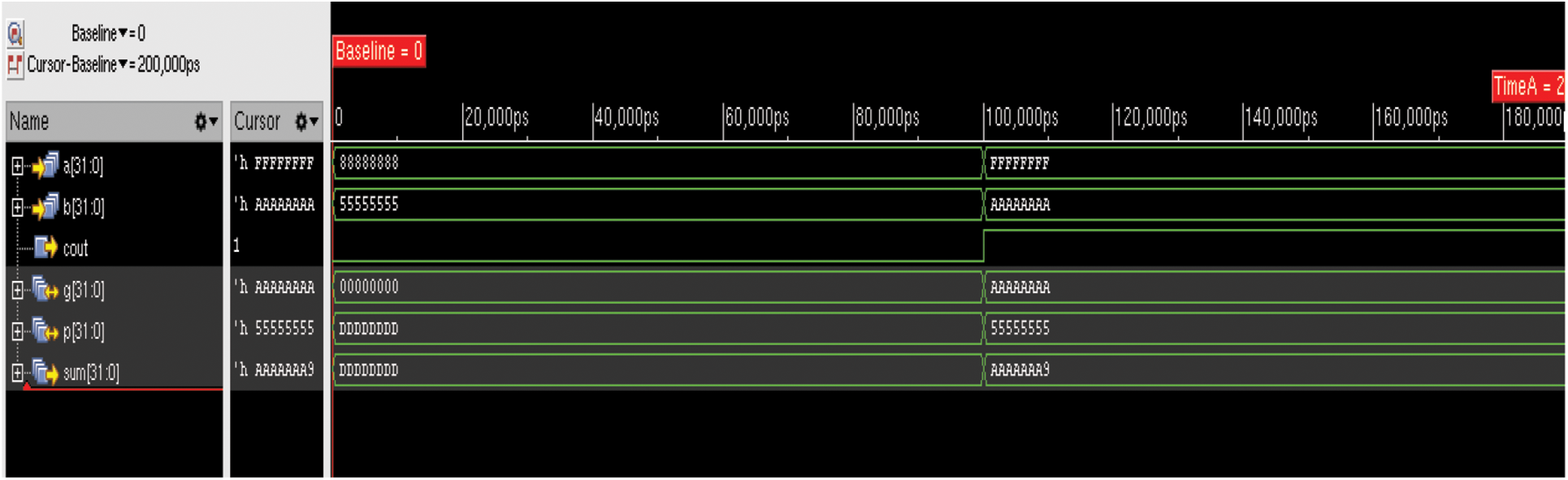
Figure 6: Simulated result for 32 Bit BSKTGT Adder
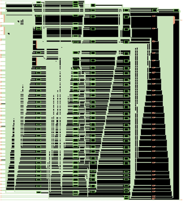
Figure 7: RTL schematic diagram of 32 Bit BSKTGT Adder
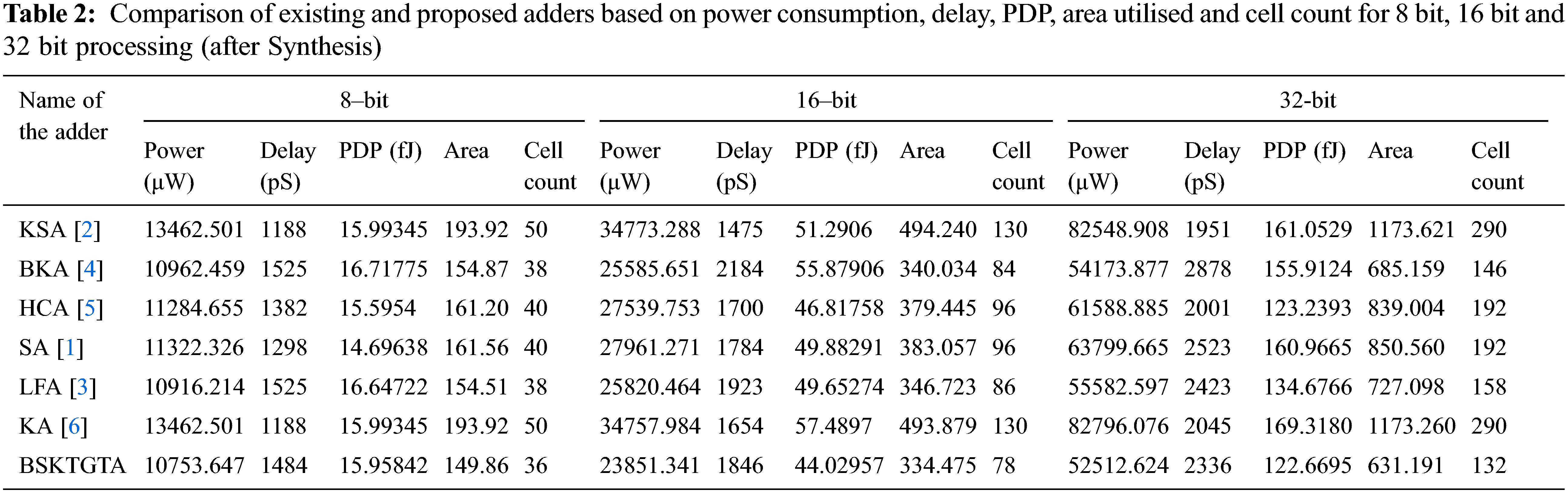
All the adders taken for the analysis in this work have been synthesised by using Cadence platform with 45 nanometre (nm) technology and the performance have been tested by measuring the area utilisation, power consumption, propagation delay, power delay product (PDP) and the cell count. The resulted values are tabulated in the following section.
Tab. 2 provides the complete analysis of 8 bit, 16 bit and 32 bit adders. Form the detailed analysis; it is very clear that the proposed BSKTGTA performs well. The detailed analysis of 32 bit adders has been included in the following section.
From Tab. 3 and Fig. 8, it is clear that, the area utilised by the proposed BSKTGTA is 631.191 which is less than BKA by 53.968, LFA by 95.907, HCA by 207.813, SA by 219.369, KA by 542.069 and KSA by 542.43.
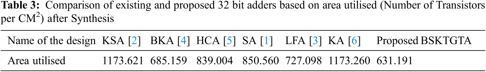
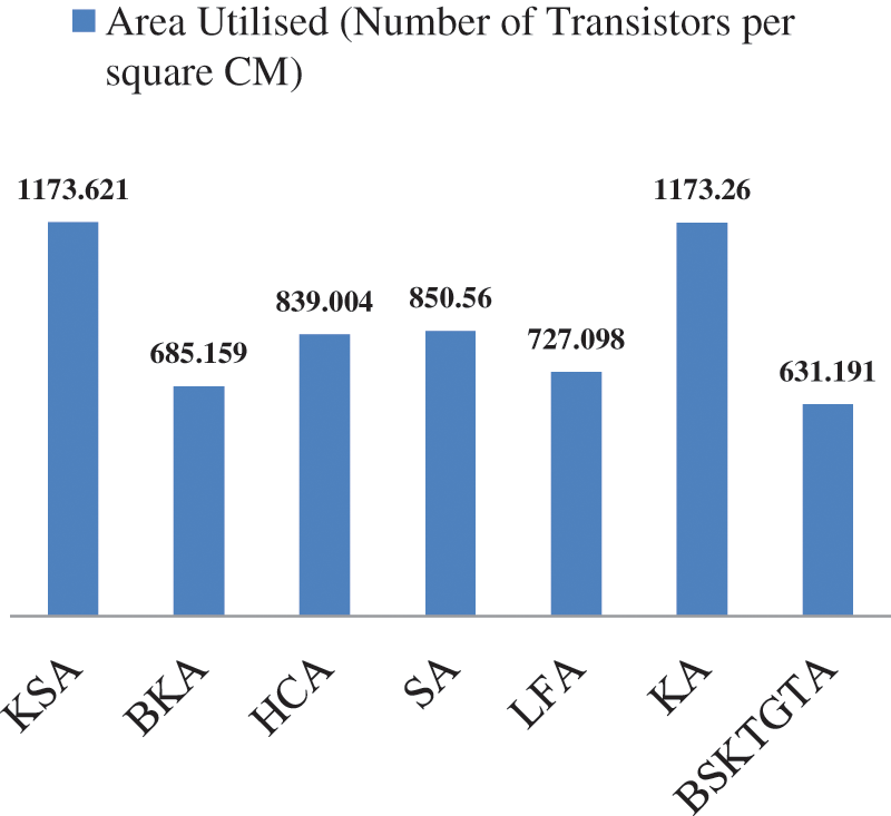
Figure 8: Area analysis of adders
From Tab. 4 and Fig. 9, it is clear that, the total power utilised by the proposed BSKTGTA is 52.512624 μW, which is 1.661253 μW lesser than BKA, 3.069973 μW lesser than LFA, 9.076261 μW lesser than HCA, 11.287041 μW lesser than SA, 30.036284 μW lesser than KSA and 30.283452 μW lesser than KA.
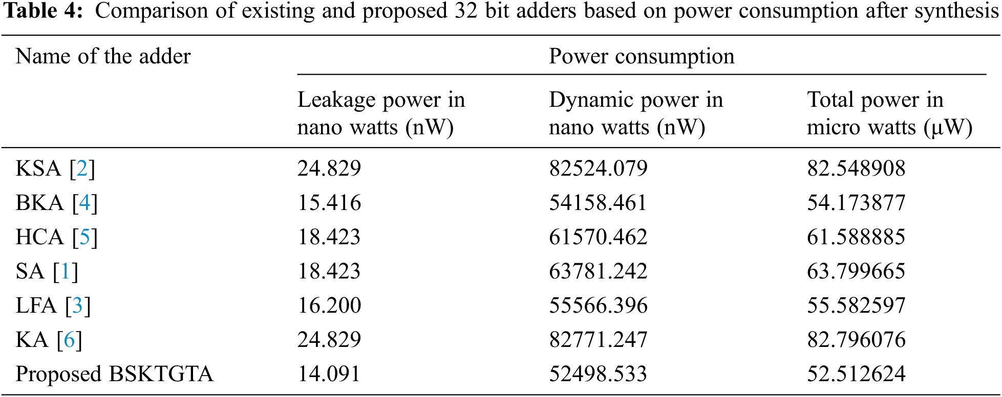
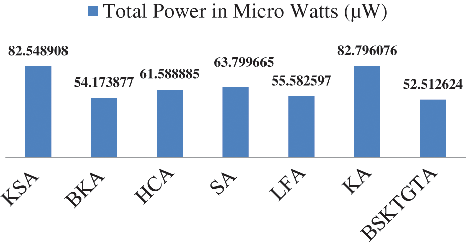
Figure 9: Power consumption analysis of adders
From Tab. 5 and Fig. 10, it is clear that, the propagation delay of proposed BSKTGTA is 2336 pS which is lesser than BKA by 542 pS, SA by 187 pS and LFA by 87 pS. Further the propagation delay of proposed BSKTGTA is higher than KSA by 385 pS, HCA by 335 pS and KA by 291 pS.
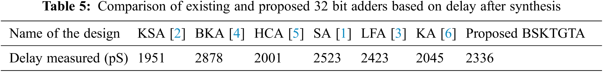
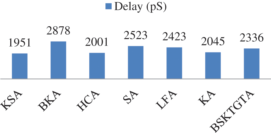
Figure 10: Delay analysis of adders
From Tab. 6 and Fig. 11, it is clear that the PDP of proposed BSKTGT adder is 122.6695 fJ, which is 0.5699 fJ lesser than HCA, 12.0071 fJ lesser than LFA, 33.2429 fJ lesser than BKA, 38.2971 fJ lesser than SA, 38.3834 fJ lesser than KSA and 46.6485 fJ lesser than KA.
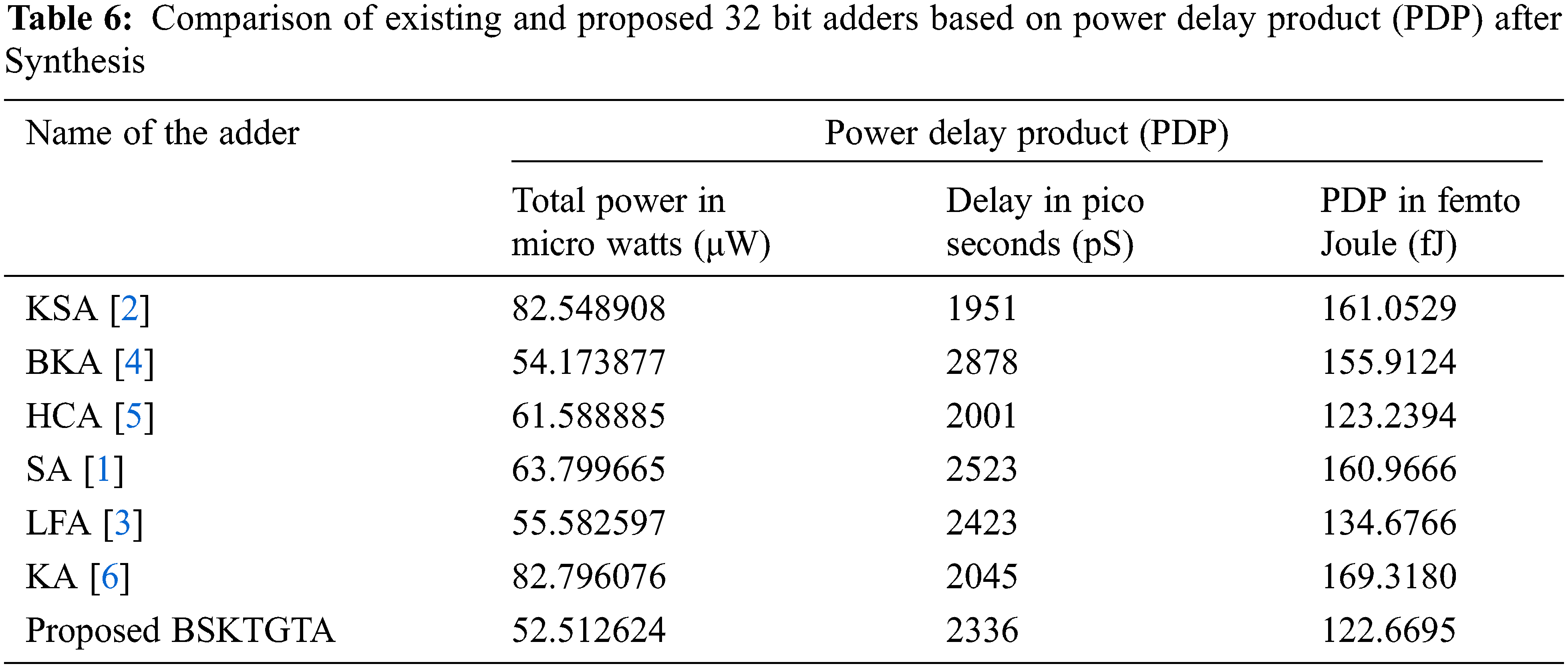
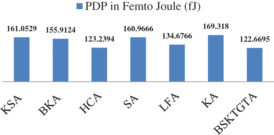
Figure 11: PDP analysis of adders
From Tab. 7 and Fig. 12, the proposed BSKTGT adder has the cell count of 132 which is 14 lesser than BKA, 26 lesser than LFA, 60 lesser than both HCA and SA, 150 lesser than both KA and KSA.
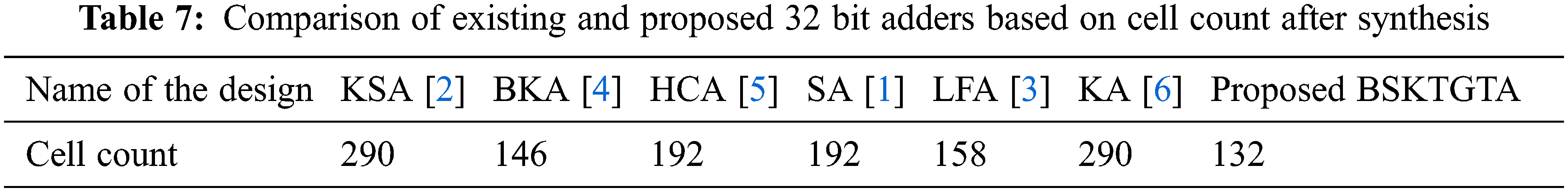
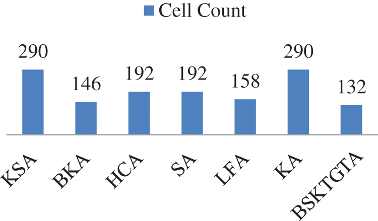
Figure 12: Cell count analysis of adders
The proposed BSKTGTA performed well in adding any 8, 16 and 32 bit values. From the results discussed, it is clear that the proposed adder has consumed 52.512426 μW which saves 3.16% of power when comparing to the Brent Kung adder which is the next best adder with the power consumption of 54.173877 μW. Similarly, the BSKTGTA utilised the area of 631.191 which is 8.55% less when comparing to the next best KSA with the area of 685.159, BSKTGTA has the cell count of 132 which is 10.61% reduction in the cell count when comparing with the next best BKA with the cell count of 146. The PDP value of proposed BSKTGTA is 122.6695 fJ, which is 0.46% less than that of the next best HCA with the PDP value of 123.2394 fJ. Further, this optimized design can be used in optical communication based applications for the replacement of existing adder and can also handle any number of input bits with the same logic.
Funding Statement: The authors received no specific funding for this study.
Conflicts of Interest: The authors declare that they have no conflicts of interest to report regarding the present study.
1. J. Li and X. Liao, “Security and privacy in new computing environments,” Mobile Networks and Applications, vol. 26, pp. 2488–2489, 2022. [Google Scholar]
2. Z. Pan, J. Sheldon and P. Mishra, “Hardware-assisted malware detection and localization using explainable machine learning,” IEEE Transactions on Computers, 2022. https://dx.doi.org/10.1109/TC.2022.3150573. [Google Scholar]
3. P. Bille, I. L. Gørtz and F. R. Skjoldjensen, “Partial sums on the ultra-wide word ram,” Theoretical Computer Science, vol. 905, pp. 99–105, 2022. [Google Scholar]
4. R. P. Brent and H. T. Kung, “A regular layout for parallel adders,” IEEE Transactions on Computers, vol. C31, no. 3, pp. 260–264, 1973. [Google Scholar]
5. Han, Tackdon and A. David Carlson. “Fast area-efficient VLSI adders,” in IEEE 8th Symposium on Computer Arithmetic (ARITH), pp. 49–56, 1987. https://zh.booksc.eu/book/22652300/864ffd. [Google Scholar]
6. G. Dimitrakopoulos, K. Papachatzopoulos and V. Paliouras, “Sum propagate adders,” IEEE Transactions on Emerging Topics in Computing, vol. 9, no. 3, pp. 1479–1488, 2022. [Google Scholar]
7. G. Dimitrakopoulos, K. Papachatzopoulos and V. Paliouras, “Sum propagate adders,” IEEE Transactions on Emerging Topics in Computing, vol. 9, no. 3, pp. 1479–1488, 2021. [Google Scholar]
8. D. Yagain, A. Vijaya Krishna and A. Baliga. “Design of high-speed adders for efficient digital design blocks,” International Scholarly Research Notices, vol. 2012, pp. 1–9, 2012. https://doi.org/10.5402/2012/253742. [Google Scholar]
9. P. Kowsalya, M. Malathi and P. Ramanathan, “Low power parallel prefix adder,” In Applied Mechanics and Materials, vol. 573, pp. 194–200, 2014. [Google Scholar]
10. S. Daphni and K. V. Grace, “Design an area efficient kogge stone adder using pass transistor logic,” in 2021 Third Int. Conf. on Intelligent Communication Technologies and Virtual Mobile Networks, Tirunelveli, India, pp. 614–618, 2015. DOI 10.1109/ICICV50876.2021.9388489. [Google Scholar] [CrossRef]
11. N. Priyadarshi, V. K. Ramachandaramurthy, S. Padmanaban and F. Azam, “An ant colony optimized MPPT for standalone hybrid PV-wind power system with single Cuk converter,” Energies, vol. 12, no. 1, pp. 167, 2019. [Google Scholar]
12. S. Daphni, and K. V. Grace, “Design and analysis of 32-bit parallel prefix adders for low power VLSI applications,” Advances in Science, Technology and Engineering Systems Journal, vol. 4, no. 2, pp. 102–106, 2019. [Google Scholar]
13. F. Elsamnah, A. Bilgaiyan, M. Affiq, C. H. Shim, H. Ishidai et al., “Comparative design study for power reduction in organic optoelectronic pulse meter sensor,” Biosensors, vol. 9, no. 2, pp. 48, 2019. [Google Scholar]
14. M. Almualla, S. Anand, M. W. Coughlin, T. Dietrich, N. Guessoum et al., “Optimizing serendipitous detections of kilonovae: Cadence and filter selection,” Monthly Notices of the Royal Astronomical Society, vol. 504, no. 2, pp. 2822–2831, 2020. [Google Scholar]
15. M. Girardi, A. Nicolò, I. Bazzucchi, F. Felici and M. Sacchetti, “The effect of pedalling cadence on respiratory frequency: Passive vs. active exercise of different intensities,” European Journal of Applied Physiology, vol. 121, no. 2, pp. 583–596, 2021. [Google Scholar]
 | This work is licensed under a Creative Commons Attribution 4.0 International License, which permits unrestricted use, distribution, and reproduction in any medium, provided the original work is properly cited. |