DOI:10.32604/iasc.2022.024770
| Intelligent Automation & Soft Computing DOI:10.32604/iasc.2022.024770 | |
| Article |
Smart Communication Using 2D and 3D Mesh Network-on-Chip
1Department of Computer Science, Teerthanker Mahaveer University, Moradabad, India
2Department of Electrical & Electronics Engineering, University of Petroleum and Energy Studies, Dehradun, 248007, India
3Government Polytechnic, Bijnor, 246276, Uttar Pradesh, India
4Faculty of Computers and Information, South Valley University, Qena, 83523, Egypt
5Department of Information Technology, College of Computer and Information Sciences, Princess Nourah bint Abdulrahman University, P.O.Box 84428, Riyadh 11671, Saudi Arabia
6Department of Mechanical Engineering, University of Petroleum and Energy Studies, Dehradun, 248007, India
*Corresponding Author: Arpit Jain. Email: dr.jainarpit@gmail.com
Received: 30 October 2021; Accepted: 12 January 2022
Abstract: Network on chip (NoC) is an integrated communication system on chip (SoC), efficiently connecting various intellectual property (IP) modules on a single die. NoC has been suggested as an enormously scalable solution to overcome the communication problems in SoC. The performance of NoC depends on several aspects in terms of area, latency, throughput, and power. In this paper, the 2D and 3D mesh NoC performance on Virtex-5 field-programmable gate array (FPGA) is studied. The design is carried in Xilinx ISE 14.7 and the behavior model is followed based on XY and XYZ routing for 2D and 3D mesh NoC respectively. The functional simulation is performed on Modelsim 10.0 software. The on-chip communicationis verified for 2D and 3D mesh NoC with different cluster sizes that pre-estimates the hardware resources utilization on FPGA. The algorithm provides a substantial platform to NoC designers to overcome the issues of substantial configuration in NoC synthesis on FPGA in case of multiple processing elements, routers, cache controllers are integrated with SoC. The suggested NoC is helpful for the embedded system design of smart wireless communication.
Keywords: Smart communication; NoC; SoC; file programmeble gate array
Design and manufacturing of Integrated Circuits (ICs) are completely dependent on integrating different sub-modules. On a single chip, these sub-modules are the pre-design blocks of Intellectual Property (IP) and cores. Any IC’s design must include the ability to reprocess. In the realm of Network-on-Chip (NoC) design and throughput, manufacturing and semiconductor businesses are experiencing new hurdles. The reuse of previously designed submodules or functional blocks is a novel approach to designing circuits with excellent performance in less time and with higher gate counts. Core-based or IP-based designs, or simple SoC designs, are based on the mentioned formalities [1]. Traditionally, the System-on-Board (SoB) technique has been used, in which each piece of work is manufactured and fabricated solely after being mounted in a discrete board. Nowadays, single chip-based SoCs are used, in which all of the cores are synthesised at the same time. Entire functional blocks are synthesized and manufactured in different units. They can be mounted on a separate board. SoB is built on pre-existing blocks. Furthermore, virtual modules, which are System-on-Chip (SoC) components, can be reused. Instead of fabricated ICs, these virtual modules are soloey used as functional logics. It encapsulates the key contrast between core-based systems and traditional design methodologies.
Many applications use bus topological structures and topologies to avoid SoC-based IPs from performing poorly. Bus-based communication systems are unable to meet bandwidth, power consumption, or latency requirements. The answer for such a communication-based system, which is a bottleneck for an embedded switching network interconnecting the different IP modules in SoCs, is NoC [2]. To maintain the arbitration mechanism and routing algorithms, as well as their implementation techniques with various communication infrastructures, the system requires more bandwidth and design space. Then, NoC plays a critical role in fault tolerance, allowing SoC designers to find the best solutions for a variety of system restrictions and characteristics. The NoC is characterized by different structures and routers connections. The way of connecting the different routers and their organization is called the topology and represented in graphical forms. The routers can be connected in the direct topology and indirect topology [3]. In the direct topology, all the routers are associated with the processor. Their combinations can be used as a single processing element in the system referred to as the nodes in the communication network. In the Indirect topology, the nodes are directly connected to the neighboring nodes with a fixed length, and messages are transferred among the nodes directly with the help of one or more instant nodes. The communication is taking place according to the different routing algorithms and routers are directly involved in the communication throughout the topology. Most of the structure is based on the orthogonal arrangement within the routers are scattered in N-Dimension and data packets move in a dimension at a particular time. Such types of arrangement are a trade-off between performance and cost, for scalableand programmable architecture [4]. Most of the popular topologies are N-Dimension mesh, torus, and hypercube.
The 2D mesh topology is configured in XY structured where ‘X’ represents the row and ‘Y’ represents the column. All the links between nodes are assumed to have an identical length, which imposes the regular structure considered in physical design for simplicity. It is also easy to predict the area requirements of mesh topology design. Moreover, the topology grows almost linearaly with increasing the number of nodes in the XY direction. In particular, the mesh topology is preferred over otheors because of its linear and physical structure. It also has the disadvantage that routers used in the mesh topology can lead the consisted region in the NoC. Due to this problem, SoC designers have to take a lot of care and applications must avoid congestion especially in the central region of the mesh. The fat tree is indirect in which the routers are not connected directly as in mesh, torus, or ring. The source and target nodes are connected in an indirect way such as in multistage networks, a crossbar switch, and tree structures. The tree topology follows the parent-child relation connecting the source to the target node. NoC is helpful for the design of smart wireless communication following different protocols such as ZigBee [5], Wi-Fi, and Bluetooth, etc. for a large-scale wireless sensor network (WSN).
The route of the signal from the source node to the destination node is decided by the router. The mesh NoC design is scalable, with the ability to establish and modify routes dynamically to improve the system’s architectural scalability. Any node in a mesh topology is free to contact any other node, either directly or through routing-capable devices relaying the message on the behalf of the message originator. If a cable segment fails, the traffic can still be diverted using the remaining wires in mesh NoC. The novelty of the work is to design the mesh NoC that supports higher frequency, throughput with minimum hardware chip parameters utilization for smart communication. The problem statement of the research paper is addressed in the same direction to design the 2D and 3D mesh NoC and analyze the performance on Virtex-5 FPGA hardware.
The rest of the paper is structured as follows. Section 2 discuss the most relevant related work. Section 3 is dedicated to the topological design of mesh NoC. The simulation results are discussed in Section 4, and finally, Section 5 concludes this research work.
NoC research is based on global communication issues in SoC, concerning the change from computation-centric to communication-centric design and providing scalable communication structures. The extensive work is done in the mesh NoC design. The systems [6] are based on an effective task migration method applicable for many-core chips configured mesh-oriented networks. The suggested algorithm gathers tasks successively working on a rectangular-shaped core. It is the source of the sub-mesh network, changes the tasks to another rectangular-shaped network, and eliminates the chip temperature hotspots to afford balanced loading condition on the chip. NoC are having the advantages [7] of using system-level synthesis and scalable design. They presented the Multi Processor System on Chips(MPSoCs) system having good performance, power, and area as a viable application explicit NoCs as more advantageous for more regular NoC topologies. NoC can be applied for the test method to diagnose online coexistent channel short and faults in traditional mesh NoC. They introduced a new method called Damaru [8] to decompose the system and provide an efficient scheduling platform without negotiating hardware resource consumption. Moreover, the proposed system scales fit with topological diversity, channel width, and network size. 2D mesh and H-star topology [9] have been used to accompany a high-performance switching architecture, also proposed the work on Birkhoff-von Neumann (BvN) switching architecture. The architecture permits the resource bandwidth that depends on a particular traffic pattern. 3D NoC architecture [10] is based on homogeneous regular mesh design integrated with compact heterogeneous floorplans as one or two separate layers. The architecture offers the benefits of compact design over regular mesh networks. The 3D NoC design provides good network performance by accumulating the mesh size, buffer size, and virtual channels. The 3-layer NoC design offered better performance compared to the 2-layer NoC architecture. The MPEG decoder has been described the increasing complexity of SoC [11] with growing the intellectual properties integrated to get the NoC efficiency, resulting in the reduction of the NoC area by 33% and reducing the power consumption by 35%.
FPGA-based simulator [12] has been used for Dynamic Partial Reconfiguration (DPR) based NoC design. The suggested design and NOC simulation examine the design constraints, limitations, and system performance parameters. It has been investigated that the system reconfiguration time increases exponentially with the increment of parallel DPRs. 3D mesh NoC (8 × 8×8) using VHDL programming in Xilinx ISE 14.2 software and synthesized the results on SPARTAN-6 FPGA [13]. The hardware results and timing values are analyzed on the same FPGA targeted device xc3s50-5-tq144 and the design supports 497.401 MHz frequency with an integrated feature of internode communication and security. Ring NoC design [14] has been suggested for Rotator-on Chip (RoC) application in which 65536 nodes were configured. The design was verified on Virtex-5 FPGA with 535.733 MHz frequency support. The priority of nodes was decided on FIFO and arbitration mechanism with 64-bit data communication. The NoC design has been evaluated the performance [15] of three on-chip communication designs and architectures for multimedia applications. The NoC architecture was configured for point-to-point (P2P) and bus-based communication in terms of space, power, and system performance. The experimental FPGA synthesis and simulation predict that bus-based communication provides poor performance in comparison to P2P in terms of chip area. The authors [16] discussed the ring NoC design concepts for different configured nodes, its simulation, and the communication of functional nodes. The performance was evaluated in terms of hardware and timing parameters using variable nodes from2 to 256 in Digilent manufactured Virtex-5 FPGA hardware. It was stated the the design supports ‘n’bit data communication and the 256-bit data was verifiedin the simulation and synthesis.
A new algorithm, Efficient Dynamic Adaptive Routing (EDAR) was used for large-scale NoC routing [17] and hardware chip implementation. The algorithm is helpful for the identification of faulty nodes in the NoC architecture. The hardware simulation results have shown good throughput and performance of EDAR in comparison to other routing algorithms. It is a suitable platform for large-scale and scalable NoC architecture to identify busy or faulty nodes. The detailed quantitative evaluation for selected dynamic process mapping algorithms for MPSoCs based on NoC structure was proposed in [18]. It can be widely varied with mesh sizes, task loads, and communication systems. They proved that the communication-aware packing-based nearest neighbor (CPNN) algorithm is having the lowest amount of energy consumption with the evaluated algorithms. The mathematical models helped for on-chip routers [19], which are based on the new model evolution of NoC performance and their analysis. The proposed router model is a group of FIFO buffers for a router with four input channels and the arrival rates of the router depend on the diagonal matrix and an average number of packets arrived at each input channel. The architectures based on the NoC topology [20] were characterized by various trade-offs about their specifications, performance, functionality, and structure. They carried the work to compare and contrast the different architectures of the NoC to estimate the hardware parameters such as latency, performance, power dissipation, and silicon area overhead. The design and assessment of a scalable and energy-efficient NoC topology [21] are based on diagonal links. The topological design is called Z-Mesh. They proposed the heuristic method for mapping the Z-Mesh design. The performance of the Z-Mesh is good for the multicast traffic routing and the link energy consumption is better in comparison to unicast-based routing. The applications and mapping are the new research issue in NoC [22]. The cores of design for particular applications are mapped to the routers in NoC topology. It affects the power requirement and overall system performance. The paper focuses on the different mapping techniques employed in the last decade. The mesh topology-based NoC has been addressed for NoC chip design [23], targeted on Virtex 6 FPGA with LX240T device. The design was based on the programmable design and priority encoder used as the scheduler. The design provides an optimized area as it is based on small buffers and follows the XY routing. The XY routing is modified based on the single buffer and used to scale large mesh NoC (8 × 8) size. The design based on a single buffer suggested the optimal solution in terms of latency and area.
Several common architectures and techniques have been discussed [24] that deal with transmission performance, system scalability, and power consumption in NoC environment. This article provides information about the layered protocol architecture of NoC as well as the routing scheme of (5 × 5) crossbar NoC. They proposed the model of BiNoC that is also known as the bi-directional NoC model. The number of channels between the two cores is not limited only up to two in the BiNoC architecture. As the number of channels will be introduced the performance will be increased. The sophisticated structure of mesh NoC is described as consisting of several segments of wires, network interfaces, and routers. Every interface can have whether source IP and destination IP. Every NoC router must have both hardware and software implementation to support the functionality of these layers. The T-mesh NoC [25] is the most popular topology that provides the complete solution to avoid the complexity of the system-on-chip. Still, there is a back draw of transmission delay in the regular mesh NoC. The author proposed a regular T-mesh topology model, which is an improved version of the mesh topology.
In the computer network, a crosspoints switch is also referred to as a crossbar switch or a switching matrix that provides multiple inputs to multiple outputs in the form of a matrix. 2D NoC router follows the crosspoint switch. The mesh NoC [26] is the structured form of (m×n) size routers. The nodes process the data in which each node consists of its processing element. One node can communicate to another with the help of a router. The NoC size of m×n represents m number of nodes in X direction and n number of nodes in Y direction. For example, let us consider (4 × 4) mesh architecture as shown in Fig. 1. To address 16 routers (2n = 16, n = 4 bit) addressing is required in which 2-bit address is for X-axis and 2-bit address for Y-axis. The selection of the routers is done based on the crosspoint addressing as listed in Tab. 1. It is called the XY routing of the 2D mesh network in which the X-axis presents the row address and Y-axis presets the column address. To understand the detailed behavior of the 2D mesh NoC, another example is considered of 64 nodes (2n = 64, then n = 6 bit) in which nodes are identified by the 3-bit address in X-axis as the row address and 3-bit address in Y-axis as column address. In the mesh NoC it is considered that all the nodes are placed at equal distance and configured in the regular structure.

Figure 1: Mesh configuration (4 × 4)

The method of XY routing is referred to as a distributed deterministic routing algorithm. XY routing never gets stuck in a stalemate or a livelock situation. The shortest and only calculated path for the packet is regularly followed by the XY routing method. The approach works fine with both regular and non-regular network topologies. The location given in the form of (x, y) is used to identify each node, where x and y represent its positions in the x- and y- dimensions respectively. No matter what the network conditions are, the path from the source node to the destination node is predetermined. In case of no traffic congestion in the NoC, it offers a high level of reliable network and a short delay. Based on XY routing, first, the packet will flow in the X-direction, then in the Y-direction, and packets cannot use any other routes to bypass blocked paths. To compute the path, the existing router (x, y) coordinate is compared to the destination router (x, y) coordinate. The router directs the signal to follow in the X-dimension and then in the Y-dimension, until the data packet reaches its target IP core.
The 3D mesh topology [27] is also configured in the same manner as the 2D mesh topology. In 3D mesh, the routing [28] is based on XYZ addressing. The diagram for 3D (3 × 3×3) mesh NoC is shown in Fig. 2 and addressing is listed in Tab. 2. In the design, 27 routers can communicate. The packet information is depicted in Fig. 3.

Figure 2: Mesh 3D-NoC (3 × 3×3)

Figure 3: Data packet format

End bit (1-bit): The status of the end bit is depicted about the ending of the transmission and it indicates that the data is received at the receiving end.
Layer Identification (3-bit): Multilayer environment is also supported by the 2D and 3D NoC. In layer identification, the addresses of the layers [29] are identified. In our case, it is assumed 3 bit, which means it can support 8 layers environment.
Sxyz (3, 3, and 3) Source Router (9-bit): It denotes the address of source routers that need to communicate based on XYZ routing. It is addressed as X (3-bit), Y (3-bit), and Z (3-bit) direction.
Dxyz (3, 3, 3) Destination Router (9-bit): It denotes the address of target routers to end the commutation as destination routers based on XYZ routing. It is addressed as X (3-bit), Y (3-bit), and Z (3-bit) direction.
Data (n-bit): It indicates the size of the data. It may be of ‘n’ bit in our case it assumed of 0 to 255 or 256-bit data.
The RTL view of the developed 2D and 3D mesh topology NoC is shown in Fig. 4. Tab. 3 discusses the use, size, and details of the pins applied to configure 2D and 3D mesh NoC. The simulation waveform is shown in Fig. 5 for 2D (4 × 4) and 3D (4 × 4 × 4) mesh NoC in binary and ASCII data formats in Modelsim software. The smart communication is verified by the simulation test case in which the source node and destination node interchange the data successfully. The depicted RTL is for the 16 nodes and 256-bit data. The nodes can vary up to 256 and data can be enhanced up to ‘n’ bit. In the simulation, the design is verified for 256-bit data among 256 nodes.

Figure 4: RTL of 2D and 3D mesh NoC

Figure 5: Modelsim results and simulation of 256-bit data in ASCII format for 2D and 3D mesh NoC

Test -1 (Mesh): First of all reset = ‘1’ and run. It will set the data of all routers and nodes to zero. Then reset = ‘0’ and give direct positive clock signal. Assign the Write_en = ‘1’, in_node_address = “001000000” out_node_address = “010000000”, X_address = “010” Y_addess = “000” and Z_address = “000” based on output node, data_in = “43 6F 6D 70 75 74 65 72 54 4D 55 40 54 4D 55 40 43 6F 6D 70 75 74 65 7254 4D 55 40 54 4D 55 40” in hexadecimal or ComputerTMU@TMU@ComputerTMU@TMU@ in ASCII. The same data is from source router R1 <255:0>. When Write_en = ‘0’, Read_in = ‘1’, the destination node R2 <255:0> and data_out <255:0> are getting the same data. Data_out = “0100 0011 0110 1111 0110 1101 0111 0000 0111 0101 0111 0101 0110 0101 0111 0010 0101 0100 0100 1101 0101 0101 0100 0000 0101 0100 0100 1101 0101 0101 0100 0000 0100 0011 0110 1111 0110 1101 0111 0000 0111 0101 0111 0101 0110 0101 0111 0010 0101 0100 0100 1101 0101 0101 0100 0000” in binary.
Write_enable and read_enable are the two control signals of the NoC which are useful to determine the access and cycle time for the data communication. The write_enable operation adds new data to the node, while the read_enable operation retrieves previously stored data. The signals are dependent on the addresses of the source and destination nodes.
The number of slices, slice flip-flops, 4 input LUTs, input/output block (IoB), and global clocks (GCLK) are the foremost critical parameters that determine hardware utilization of NoC. The values are taken straight from the Xilinx software summary. The hardware parameters help the designer to estimate the Virtex-5 FPGA hardware resource utilization and pre-estimates the values in pre-synthesis of the NoC. The hardware resources are estimated for different mesh configurations in which the nodes are configured in maximum cluster size (8 × 8) in which 256 nodes can communicate to each other. The FPGA hardware and timing performance parameters [30] are listed for 2D NoC in Tabs. 4 and 5. Figs. 6 and 7 present the hardware and timing utilization graph for 2D mesh NoC respectively. In the same way, the FPGA hardware and timing performance parameters [31] for 3D NoC are listed in Tabs. 6 and 7. Figs. 8 and 9 present the hardware and timing utilization graph for 3D mesh NoC respectively. The data presents that the hardware and time delay is increasing as the network cluster configuration is increasing.

Figure 6: Hardware utilization with cluster size in 2D mesh NoC

Figure 7: Timing values with cluster size in 2D mesh NoC

Figure 8: Hardware utilization with cluster size in 3D mesh NoC

Figure 9: Timing values with cluster size in 3D mesh NoC


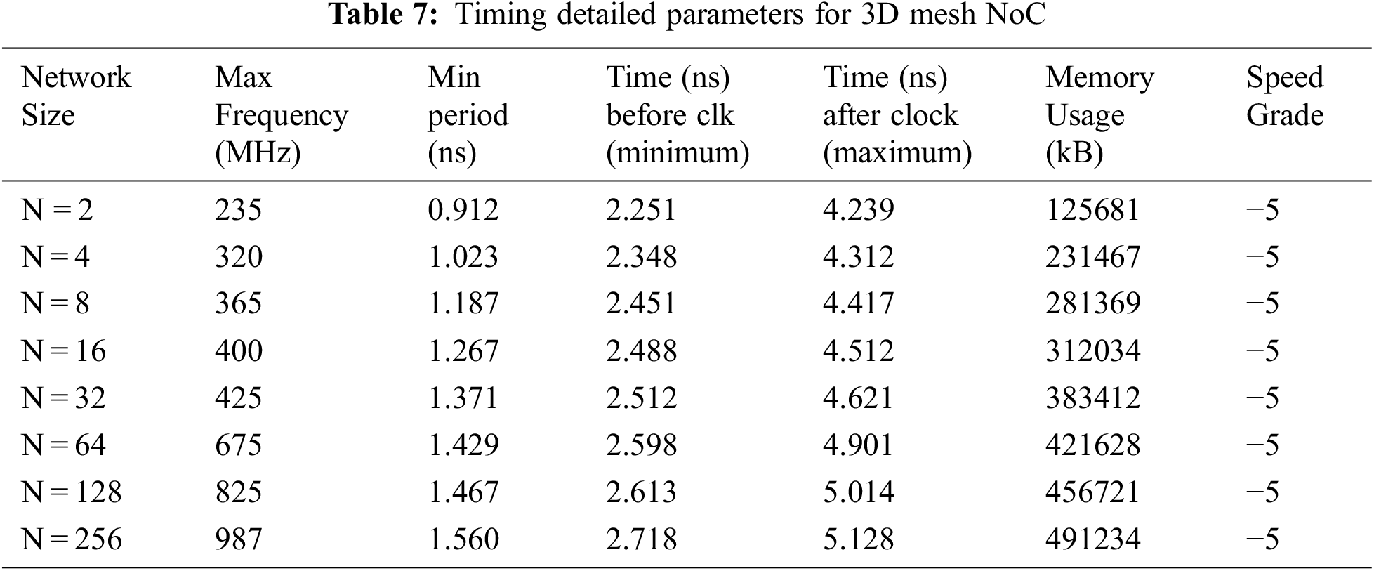
In the 2D mesh design, the number of the flip-flops are 34, 39, 52, 60, 72, 78, 86, and 104 for the different sizes of mesh NoC. In 3D mesh design, the number of the flip-flops are 33, 36, 50, 57, 69, 75, 83, and 102 for the different sizes of mesh NoC. The number of slices are increasing as the nodes are increasing and hardware complexity is increasing. It indicates that the 3D mesh consumes fewer hardware resources than the 2D mesh. The hardware utilization is increasing as the node cluster size is increasing in the 2D and 3D NoC. It will rise in tandem with the design complexity. In 2D and 3D NoC, the clock latency appears to be growing with the number of nodes. The frequency support of the 3D mesh NoC is greater than that of the 2D, indicating that the 3D NoC is the best option in terms of hardware specifications and frequency support.
The NoC design and FPGA implementation are facing the challenge of SoC communication integration on-chip die. The probability of failure in NoC is increasing with the rapid shrinking of chip die size. Furthermore, the arbitrary positions may affect the uniformity of actual topological design, and a fixed NoC can become irregular. The intercommunication among numerous cores and IP modules on the singlechip may affect the system performance and communication of the chip as throughput, area, power, and latency are the critical issues of chip design. In the research work, 2D mesh (4 × 4) and 3D mesh (3 × 3 × 3) NoC are designed successfully in Xilinx ISE 14.7 and simulated using Modelsim 10.0. The XY and XYZ routing are followed to address the nodes in 2D and 3D mesh NoC. FPGA is a scalable device, which provides the synthesis environment with different clusters size of NoC. The FPGA is configured for mesh topology structure for different cluster sizes (N = 2, 4, 8, 16, 32, 64, 128, 256) that supports 2D mesh (16 × 16) and 3D mesh (8 × 8 × 8) design in which 256 nodes can communicate each other. For semiconductor industries, the hardware resource utilization and timing parameters are the critical aspects. This study will help the NoC designers to plan before designing the chip itself by considering the known hardware design factors, memory utilization, and timing parameters to configure large-scale NoC. In the case of designing a large-scale Wireless Sensor Network, the suggested mesh NoC design aids hardware designers in estimating FPGA resource utilization for smart computing and control applications.
Acknowledgement: This research project was funded by Princess Nourah bint Abdulrahman University Researchers Supporting Project number (PNURSP2022R51), Princess Nourah bint Abdulrahman University, Riyadh, Saudi Arabia.
Funding Statement: The authors received no specific funding for this study.
Conflicts of Interest: The authors declare that they have no conflicts of interest to report regarding the present study.
1. A. Hussain, M. Irfan, N. K. Baloch, U. Draz, T. Ali et al., “Savior: A reliable fault resilient router architecture for network-on-chip,” Electronics, vol. 9, no. 11, pp. 1783–1790, 2020. [Google Scholar]
2. X. Feng, Q. Zhuo, X. Liu, Y. Qian and Y. Li, “Development of multi-motor synchronous control system based on network-on-chip,” Journal of Systems and Control Engineering, vol. 234, no. 9, pp. 1000–1010, 2020. [Google Scholar]
3. H. C. Touati and F. Boutekkouk, “Reliable weighted globally congestion aware routing for network on chip,” International Journal of Embedded and Real-Time Communication Systems, vol. 11, no. 3, pp. 48–66, 2020. [Google Scholar]
4. A. Jain, A. Kumar and S. Sharma, “Comparative design and analysis of mesh, torus and ring NoC,” Procedia Computer Science, vol. 48, pp. 330–337, 2015. [Google Scholar]
5. L. Chhaya, P. Sharma, G. Bhagwatikar and A. Kumar, “Wireless sensor network based smart grid communications: Cyber-attacks, intrusion detection system and topology control,” Electronics, vol. 6, no. 1, pp. 5–22, 2017. [Google Scholar]
6. S. Afsharpour, A. Patooghy and M. Fazeli, “Performance/energy-aware task migration algorithm for many-core chips,” IET Computers & Digital Techniques, vol. 10, no. 4, pp. 165–173, 2016. [Google Scholar]
7. D. Atienza, F. Angiolini, S. Murali, A. Pullini, L. Benini et al., “Network-on-chip design and synthesis outlook,” Integration, vol. 41, no. 3, pp. 340–359, 2008. [Google Scholar]
8. B. Bhowmik, J. K. Deka, S. Biswas and B. B. Bhattacharya, “Performance-aware test scheduling for diagnosing coexistent channel faults in topology-agnostic networks-on-chip,” ACM Transactions on Design Automation of Electronic Systems (TODAES), vol. 24, no. 2, pp. 17–21, 2019. [Google Scholar]
9. Y. C. Chang and C. T. Chiu,“A study of NoC topologies and switching arbitration mechanisms,” in Proc. of IEEE 14th Int. Conf. on High Performance Computing and Communication & 2012 IEEE 9th Int. Conf. on Embedded Software and Systems, Liverpool, UK, pp. 1643–1647, 2012. [Google Scholar]
10. V. D. Paulo and C. Ababei, “3D Network-on-chip architectures using homogeneous meshes and heterogeneous floorplans,” International Journal of Reconfigurable Computing, vol. 2010, no. 603059, pp. 1–12, 2010. [Google Scholar]
11. A. Hansson, K. Goossens and A. Rădulescu, “A unified approach to mapping and routing on a network-on-chip for both best-effort and guaranteed service traffic,” VLSI Design, vol. 2007, no. 68432, pp. 1–17, 2007. [Google Scholar]
12. A. Hassan, H. Mostafa and H. A. Fahmy, “NoC-DPR: A new simulation tool exploiting the dynamic partial reconfiguration (DPR) on network-on-chip (NoC) based FPGA,” Integration, vol. 63, pp. 204–212, 2018. [Google Scholar]
13. A. Kumar, G. Verma, M. K. Gupta, M. Salauddin, B. K. Rehman et al., “3D multilayer mesh NoC communication and FPGA synthesis,” Wireless Personal Communications, vol. 106, no. 4, pp. 1855–1873, 2019. [Google Scholar]
14. A. Kumar, L. Baruha and A. Sabu, “Rotator on-chip (RoC) design based on ring topological NoC,” Procedia Computer Science, vol. 45, pp. 540–548, 2015. [Google Scholar]
15. H. G. Lee, N. Chang, U. Y. Ogras and R. Marculescu, “On-chip communication architecture exploration: A quantitative evaluation of point-to-point, bus, and network-on-chip approaches,” ACM Transactions on Design Automation of Electronic Systems (TODAES), vol. 12, no. 3, pp. 1–20, 2008. [Google Scholar]
16. A. Jain, R. K. Dwivedi, H. Alshazly, A. Kumar, S. Bourouis et al., “Design and simulation of ring network-on-chip for different ConfiguredNodes,” Computers, Materials & Continua, vol. 71, no. 2, pp. 385–4100, 2022. [Google Scholar]
17. J. Liu, J. Harkin, Y. Li and L. Maguire, “Low cost fault-tolerant routing algorithm for networks-on-chip,” Microprocessors and Microsystems, vol. 39, no. 6, pp. 358–372, 2015. [Google Scholar]
18. T. Maqsood, S. Ali, S. U. Malik and S. A. Madani, “Dynamic task mapping for network-on-chip based systems,” Journal of Systems Architecture, vol. 61, no. 7, pp. 293–306, 2015. [Google Scholar]
19. U. Y. Ogras, P. Bogdan and R. Marculescu, “An analytical approach for network-on-chip performance analysis,” IEEE Transactions on Computer-Aided Design of Integrated Circuits and Systems, vol. 29, no. 12, pp. 2001–2013, 2010. [Google Scholar]
20. P. P. Pande, C. Grecu, M. Jones, A. Ivanov and R. Saleh, “Performance evaluation and design trade-offs for network-on-chip interconnect architectures,” IEEE Transactions on Computers, vol. 54, no. 8, pp. 1025–1040, 2005. [Google Scholar]
21. N. Prasad, P. Mukherjee, S. Chattopadhyay and I. Chakrabarti, “Design and evaluation of Z-mesh topology for on-chip interconnection networks,” Journal of Parallel and Distributed Computing, vol. 113, pp. 17–36, 2018. [Google Scholar]
22. P. K. Sahu and S. Chattopadhyay, “A survey on application mapping strategies for network-on-chip design,” Journal of Systems Architecture, vol. 59, no. 1, pp. 60–76, 2013. [Google Scholar]
23. P. Shahane and N. Pisharoty, “Modified XY routing for mesh topology based NoC router on field programmable gate array,” IET Circuits, Devices & Systems, vol. 13, no. 3, pp. 391–398, 2019. [Google Scholar]
24. W. C. Tsai, Y. C. Lan, Y. H. Hu and S. J. Chen, “Networks on chips: Structure and design methodologies,” Journal of Electrical and Computer Engineering, vol. 2012, no. 509465, pp. 1–16, 2012. [Google Scholar]
25. Q. Yang and Z. Wu, “An improved mesh topology and its routing algorithm for NoC,” in Proc. Int. Conf. on Computational Intelligence and Software Engineering, Wuhan, China, pp. 1–4, 2010. [Google Scholar]
26. A. Kumar, P. Sharma, M. K. Gupta and R. Kumar, “Machine learning-based resource utilization and pre-estimation for network on chip (NoC) communication,” Wireless Personal Communications, vol. 102, no. 3, pp. 2211–2231, 2018. [Google Scholar]
27. A. Jain, R. Dwivedi, A. Kumar and S. Sharma, “Scalable design and synthesis of 3D mesh network on chip,” Advances in Intelligent System Computing, vol. 479, pp. 661–666, 2017. [Google Scholar]
28. N. Gupta, A. Jain, K. S. Vaisla, A. Kumar and R. Kumar, “Performance analysis of DSDV and OLSR wireless sensor network routing protocols using FPGA hardware and machine learning,” Multimedia Tools and Applications, vol. 80, no. 14, pp. 22301–22319, 2021. [Google Scholar]
29. A. Jain, A. K. Gahlot, R. Dwivedi, A. Kumar and S. K. Sharma, “Fat tree NoC design and synthesis,” Intelligent Communication, Control and Devices, vol. 624, pp. 1749–1756, 2018. [Google Scholar]
30. A. Jain, R. Dwivedi, A. Kumar and S. Sharma, “Network on chip router for 2D mesh design,” International Journal of Computer Science and Information Security, vol. 14, no. 9, pp. 1092–1099, 2016. [Google Scholar]
31. V. M. M. Ompal and A. Kumar, “Zigbee internode communication and FPGA synthesis using mesh, star and cluster tree topological chip,” Wireless Personal Communications, vol. 119, pp. 1321–1339, 2021. [Google Scholar]
 | This work is licensed under a Creative Commons Attribution 4.0 International License, which permits unrestricted use, distribution, and reproduction in any medium, provided the original work is properly cited. |