DOI:10.32604/iasc.2022.024804
| Intelligent Automation & Soft Computing DOI:10.32604/iasc.2022.024804 | |
| Article |
Smart Grid Security by Embedding S-Box Advanced Encryption Standard
1Department of Electronics & Communication Engineering, Uttarakhand Technical University, Dehradun, India
2Department of Electrical Engineering, G. B. Pant Engineering College, Pauri-Garhwal, Uttarakhand, India
3Department of Electrical & Electronics Engineering, School of Engineering, University of Petroleum and Energy Studies, Dehradun, India
*Corresponding Author: Niraj Kumar. Email: neeraj_mmmec@yahoo.com
Received: 31 October 2021; Accepted: 04 January 2022
Abstract: Supervisory control and data acquisition (SCADA) systems continuously monitor the real-time processes in the smart grid. The system software, which is based on a human-machine interface (HMI), makes intelligent decisions to assist the system operator and perform normal grid management activities. The management of SCADA networks and monitoring without proper security is a major concern, as many grids and plant networks still lack necessary monitoring and detection systems, making them vulnerable to attack. SCADA networks exploit physical weaknesses as well as cyber-attacks. Researchers have developed a monitoring system based on a field-programmable gate array (FPGA) and a microcontroller that allows for faster timing and system response. The cryptography-based substitution box (S-box) Advanced Encryption Standard (AES) and decryption method were proposed in the research paper, which may be merged with smart grid communication hardware and grid distribution as an integrated chip, synthesized on FPGA-Virtex-5 hardware. The method creates a platform for grid security by implementing a cryptographic-based security algorithm in hardware chips. The algorithm was designed using VHDL coding in Xilinx ISE 14.7 software and tested with various grid data sizes and key. The research represents a significant effort on the part of the businesses looking for solutions to secure the smart grid and plants by incorporating secure hardware.
Keywords: Smart grid cybersecurity; cryptography encryption; FPGA verification; S-box AES algorithm; VHDL programming
The smart grid [1] is the advanced electrical grid that provides a bidirectional communication set-up and enables digital information and communication technologies (ICTs) between the utility and its consumers at any level of electricity generation, transmission to an electrical substation, distribution, and energy consumption. Smart grids like the Internet, feature smart control, automation, computers, new technologies, and related equipment that work together digitally on an electrical grid to meet the needs of the grid and users. The main constituents of the smart grid are embedded smart sensors, smart meter (SM), phasor measurement unit (PMU), information processing from the physical environment to a sensor network, and wireless sensor network (WSN). The smart grid [2] epitomizes unique prospects to propel the electricity industry into a new era of availability [3], dependability, and confidentiality, all of which can help the country's economic growth and environmental health. The smart grid includes efficient electricity transmission [4], increased security, faster restoration of power instabilities and electricity, low-cost operations and maintenance, low-cost service to consumers, reduced peak demand, and larger-scale integration of various renewable energy [5] resources.
The National Institute of Standards and Technology (NIST) [6] is working on the smart grid standards, selection, and identification requirements proposed in 2007 by the Energy Independence and Security Act (EISA). The Federal Energy Regulatory Commission (FERC) refers to the NIST standards for smart grid communication, infrastructure, and standardization. A smart grid is divided into seven logical domains [7] according to NIST: bulk generation, transmission, distribution, customer, markets, service provider, and operations. These domains contain actors and applications that use devices, as well as systems in which a single actor in the domain completes the applications. Fig. 1 presents the conceptual model of the smart grid [8] and its interface of actors within domains with the use of a secure channel. For two-way information interchange and power flow, the bulk generation of electricity, transmission to the substation, distribution, and customers are required [9]. The primary components of power management and data communication are market availability, servicing, and operations.
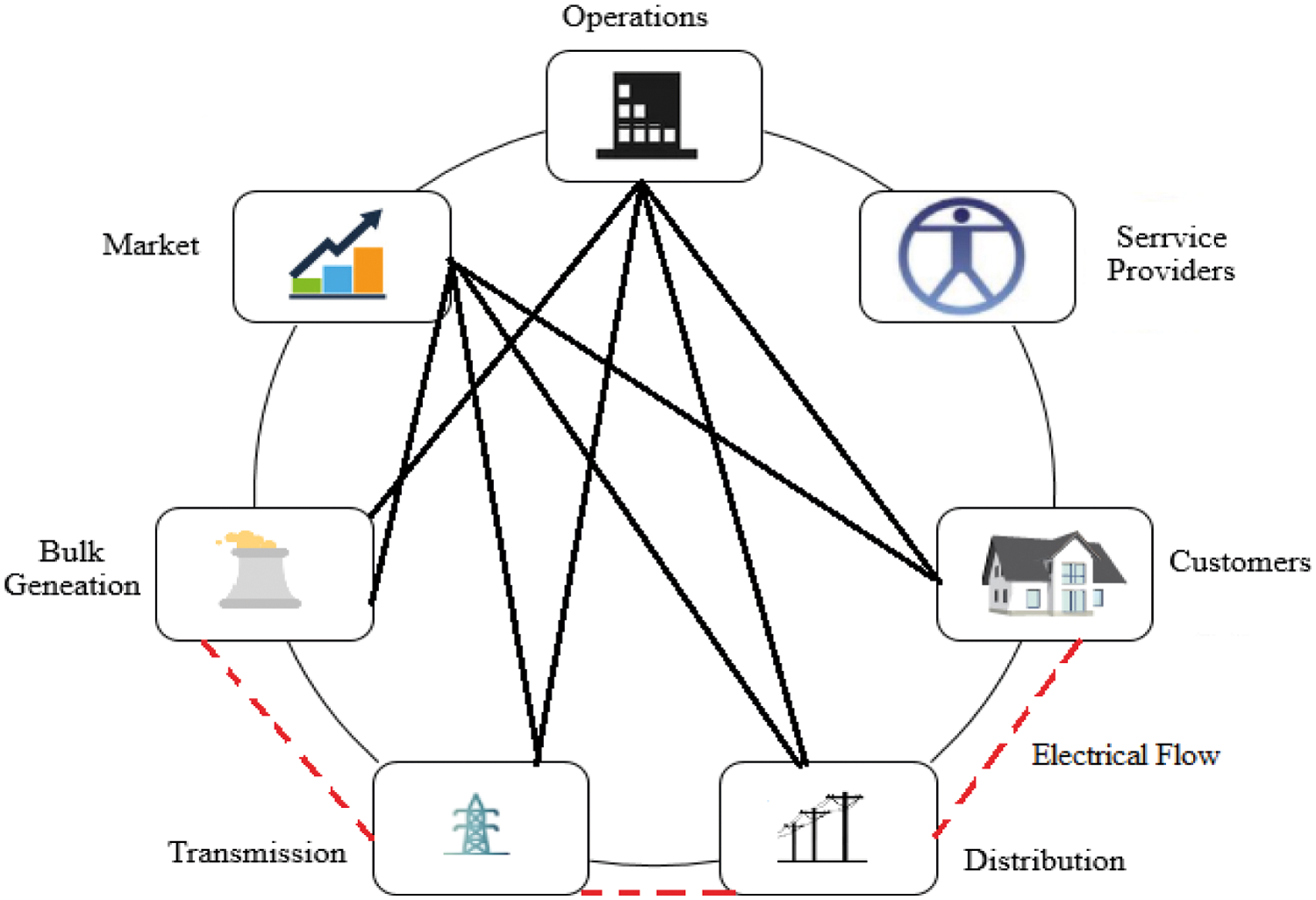
Figure 1: NIST conceptual model for smart grid
Fig. 2 depicts the smart grid backbone and local area network (LAN), with solar, wind, and plant generation and transmission falling under the wide-area network (WAN), distribution falling under the neighborhood area network (NAN), and consumers falling under the home area network (HAN). SCADA [11] is used to provide a service that allows users to remotely monitor and manage network equipment to satisfy customer demand and improve reliability. The SCADA systems encourage cybersecurity [12] in the smart grid, tempting the vulnerability, as numerous locations are spread out over a large distance and use ICT. The current SCADA system includes a human-machine interface (HMI) for data processing and administration, supervisory distributed computer control (SDCC) for data collecting and run processing, and a remote terminal unit (RTU) for long-distance updates. The system is connected to the grid using certain dedicated lines, and an internet subsystem.
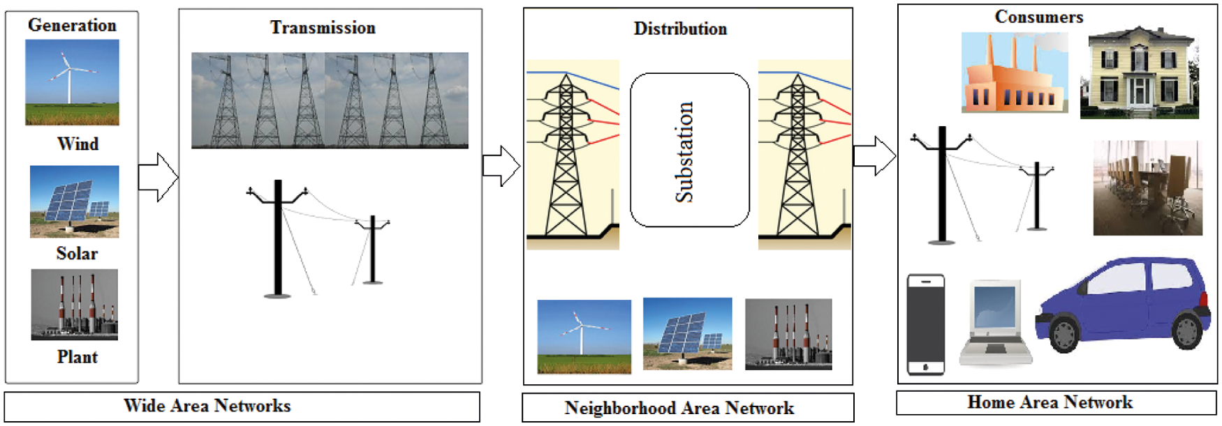
Figure 2: LANs and backbone for smart grid communication network architecture [10]
Offsite electrical energy distribution via nuclear power plant (NPP) [13] switchyards and the electrical transmission grid has been considered as one of the safest and most dependable electrical energy transmission options for safe work and accident mitigation at NPPs. The digital smart grid revolution and application of digital smart grid technologies in operations has raised the grid's operating and design requirements, including but not limited to safety, dependability, cybersecurity [14], and stability [15], which includes nuclear power plants. The nuclear power plants come in the category of bulk generation domain when evaluating the communications links and necessities of smart grid interoperability requirements. It consists of the power transmission, operations, markets, and distribution unit, which allows the transmission grid and distribution system to interact in the smart grid. Nuclear power stations have the potential to produce clean energy industries and will be an integral part of the smart grid's future infrastructure. Grid failures, natural disasters, terrorism, human factors, attackers, and other reasons can cause disruptions [16] in smart grid operations. Therefore, it is essential to contemplate the security of the smart grid and make strategies to avoid hardware and software vulnerabilities. FPGA chips have been applied widely for 20 years for instrumentation and operation control in nuclear plant industries and complex electronic devices [17]. The advantage of FPGA technology is that the safety assessment techniques and risks in plant instrumentation and control can be experienced at a programmable platform. Moreover, intelligent conditional monitoring techniques and neural networks can be used for plant operations. Sparse auto-encoder [18] has been applied for feature extraction and dimensionality reduction. The isolation forest is applied for the abnormality and anomaly monitoring in NPP. For the past 20 years, FPGA chips have been widely used in nuclear plant sectors and complicated electronic equipment for instrumentation and operation control. The FPGA was utilized in the power plant for GSM-based wireless monitoring [19] that enabled security and message authentication on the mobile that kept the boiler temperature, pressure, and loads below the threshold limits.
The SCADA system [20] is in charge of keeping the underlying communication secure between substations and the accompanying control center in the smart grid. Some security methods do not match with the smart grid's full security standards when communication is taken place between customers and substations. The design of appropriate authentication and the secured system is a difficult challenge due to the complex nature of the smart grid and different security requirements. The group signature system [21] is a widely used cryptographic base for privacy protection that does not expose the identity of the user but does establish that the candidate is a valid user. A password-based authentication mechanism was devised to strengthen the security of the smart grid [22], and it may be used not only on expandable test sites but also on power plants, including nuclear power plants. The group signature scheme is an anonymous signature technique in which the authenticator checks the group signature to see if the signer is a member of a specific group, but does not have an idea who signed in. The advantage of FPGA is that it provides faster switching in comparison to a programmable logic controller (PLC) and microcontrollers. The cryptography-based encryption and decryption methods were used to protect the smart grid sensitive data [23] from being altered or stolen. The key size and data size play an important role in the cryptography-based operation. The cryptography algorithms have limited key lengths. The suitability of the specific algorithm, hardware implementation in SACDA, and smart grid is a challenging task. In many SCADA systems, the AES algorithm [24] has been demonstrated to be the optimal method for hardware security. The 128-bit AES algorithm was realized on Spartan-3E FPGA with the complete detail of hardware and timing parameters summary for smart grid security [25]. The AES implementation approach and architecture influence chip hardware utilization, speed, performance, size, power consumption, and security. Time authenticated cryptographic identity transmission (TACIT) algorithm [26] was tested on the FPGA platform for 64-bit encryption and decryption. The algorithm was successfully evaluated for on-grid parameters and nuclear plant operations using 64-bit and 128-bit key sizes [27]. The AES encryption-based system hardware algorithm improves security and safety. In comparison to the traditional AES method, the current AES algorithm with S-box [28] has demonstrated good hardware and timing performance.
The smart power grids provide two-way networks that connect generators to consumers using cutting-edge smart technology, assisting cities in their transition to low-carbon electricity sources while also ensuring stable, reliable, and long-term energy supplies. SCADA systems are more sensitive to cyber-attacks and data theft from the grid. Grid security can be improved by employing the notion of cryptography, which encrypts and decrypts grid data using modern cryptography algorithms. The use of such embedded hardware improves the confidentiality of the grid. In symmetric key algorithms, the same key is used on both the sending and receiving ends, whereas, in asymmetric ley algorithms, the private key is used on both sides. DES and AES are examples of symmetric key cryptography. Instead of using the traditional AES technique, the modified multiplexer-based S-box approach can be employed to save time and space while maintaining throughput. The problem statement of the research work is to realize the latest multiplexed S-box-AES algorithm on FPGA hardware and analyze the hardware performance for smart grid and plant applications.
AES [29] is a data encryption and decryption method that is used to offer security over a network. It was one of the most popular algorithms given by NIST in 2001, and Rijndael gave its original name.
The AES mathematical method was created by two well-known Belgian cryptographers, Vincent Rijmen and Joan Daemen [30], and is based on the Rijndael block cipher method. They presented the method to NIST during the AES selection process. The Rijndael structure is cryptography, cipher family that supports various key, and block sizes. The AES algorithm is one of the most widely used symmetric encryption techniques. The AES algorithm [31] is at least six times faster and more reliable than the previously introduced data encryption standard (DES) and triple-DES [32]. Because the key length of the DES cryptographic method was so little, an auxiliary algorithm was required so that computational power could be increased in hardware applications and grid operation will become faster. The algorithm has been considered more susceptible in contradiction of attacks and provides security with different key lengths. Fig. 3 depicts the AES encryption text processing and procedure. The algorithm has the following features.
• The AES method is much stronger and faster than triple-DES [33].
• It is based on symmetric block cipher technique [34] and key distribution is symmetric
• The block data length is available up to 128-bit data, and key size is varying 128/192/256 bit [35].
• Its architecture is scalable and provides full custom design specifics and particulars
• The method can be implemented in hardware and software using Java, C, a hardware description language (HDL) environment, and an integrated development environment (IDE).
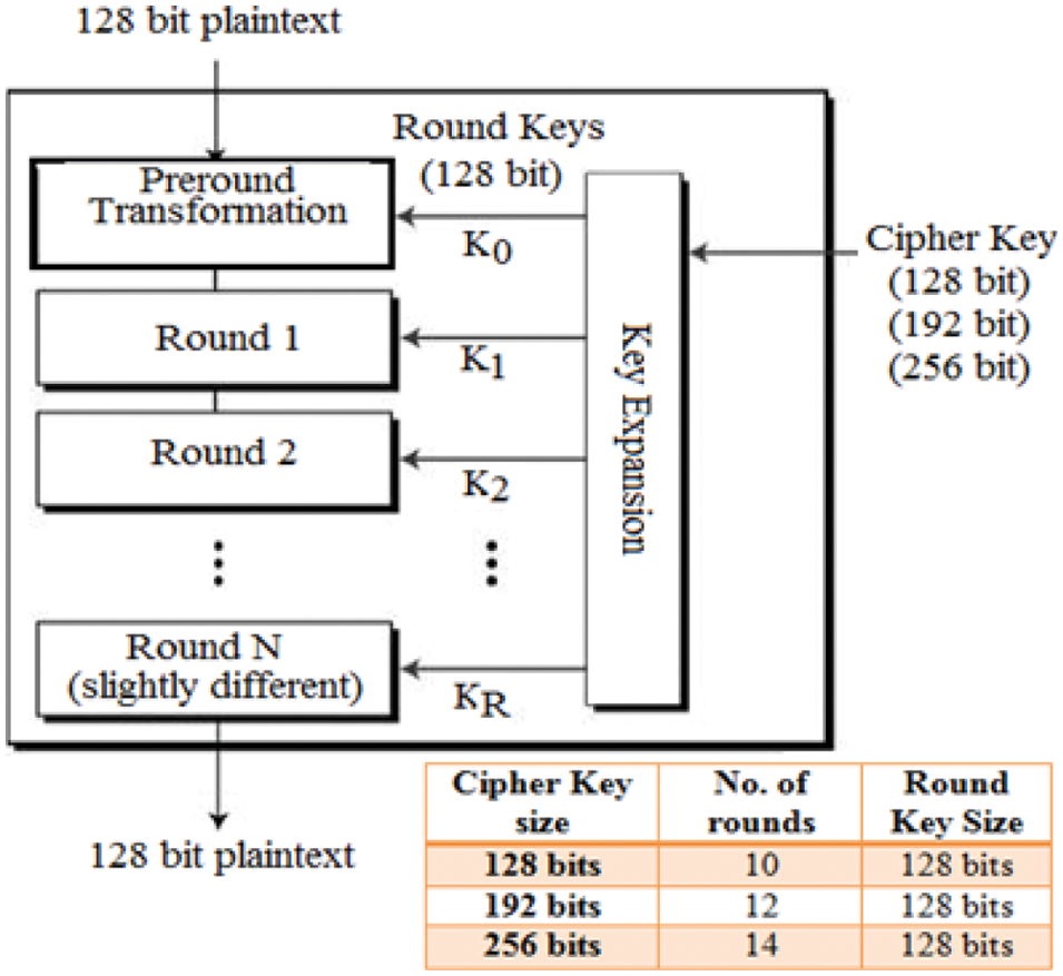
Figure 3: Key expansion in AES [30]
The complete flow of the AES algorithm is shown in Fig. 4 which includes the actions of reading plain text, adding a circular key, performing a sub-byte operation, shifting rows, mixing columns for one round key, and proceeding to the last round of key. Fig. 5 depicts the 128-bit key operation using AES encryption.
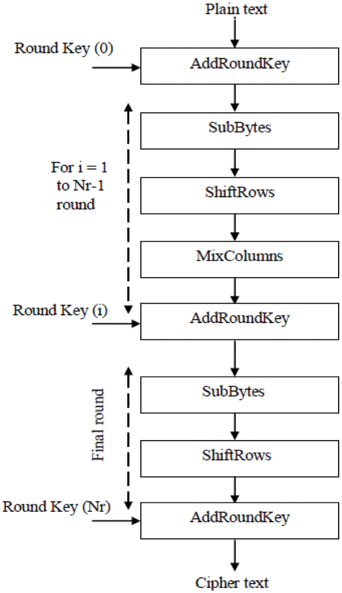
Figure 4: Flow of AES algorithm [36]
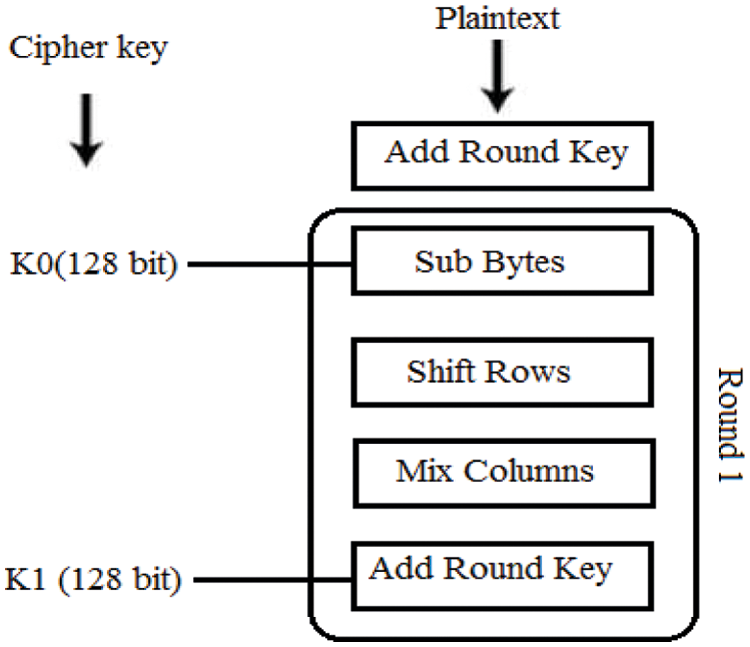
Figure 5: AES encryption process for 128-bit key [36]
Encryption
The AES encryption algorithm works on the rounding operation. The operation is completed in four sub-processes. The initial circular or round operation is described as follows:
Byte-substitution (Sub-bytes): The algorithm is 6 bytes long and follows the fixed table of the S-box matrix of the design. It creates a (4 × 4) matrix with four columns and four rows
Shift-rows: The elementary row of the matrix is moved to the left side. The descent off access after shift operation is further considered from the right side. The shifting operation is followed as
• No shift operation is considered in the initial row
• The left shift process is considered for the 2nd row and the data is shifted to the left position by a 1-byte operation.
• A similar process is followed for the third shifted row to the left side by 2-byte sequential processing.
• The 4th-row shift operation is done towards the left-hand side followed by 3-byte positions
• This shift operation forms one matrix
• The new resultant matrix is formed by 16-bytes values generated by shifting the contents for one another.
Mix-columns: The distinct mathematical operation is followed for 4-bytes in each column. This procedure takes all 4-bytes of a single column as inputs and outputs entire new 4-bytes, which can change the values in the main column. A new matrix with 16-bytes is created using this procedure. It should be noted that none of these alternatives were used in the previous round.
Add-round-key-operation: The 128-bit block takes 16 bytes of operation, and the bitwise XOR technique is used to extend the key length beyond 128-bit. The ciphertext is generated in the final round process. The 128-bit result is treated as an additional 16 bytes, and a similar rounding operation is carried out for the same length of key size and block data.
Decryption
The decryption process is carried out in the same way as the encryption process, except all phases are carried out in the opposite direction. The first operation in the decryption procedure is the process that is finished at the end of encryption. All four steps are well thought out in converse sequence for each subsequent round. Add round key operation » mix columns » shift rows » byte substitution. All of the steps in the decryption method are reversed, just like in AES encryption. Sub byte, shift row, mix column, and Add round key [37] in regular rounds are the four major operations of the method. The following features are taken into account in the hardware design
• Segregation of shift row transformation
• Pipelined structure for higher throughput with pipelining and parallel operation
• Design optimization to keep convenient stability between output and silicon area
Segregation of shift row transformation
It is unbiased direction-finding in the face of information and receipts that have no place in the design. Shifting elementary contents from the design matrix achieves shift row segregation. It can be used instead of calling components one by one from the data matrix in a sequential fashion. As a result, the one-step operation is reduced by merging the two-step operations of shift-row and sub-byte. Fig. 6 depicts the process of removing the shift row. In each round, the 16 elements are preserved one by one and saved consecutively in a record file. The design is based on multiplexer selection, which is required to shift numbers and elements from the recorded register file and deposit them sequentially into the S-box. The row transformation of AES is shown in Fig. 7. The concept of sub byte transformation (S-box) is possible to implement using LUT as shown in Fig. 8. It is a more efficient and well-organized technique that may be used directly to implement the multiple contrary operations offered by an affine transformation.
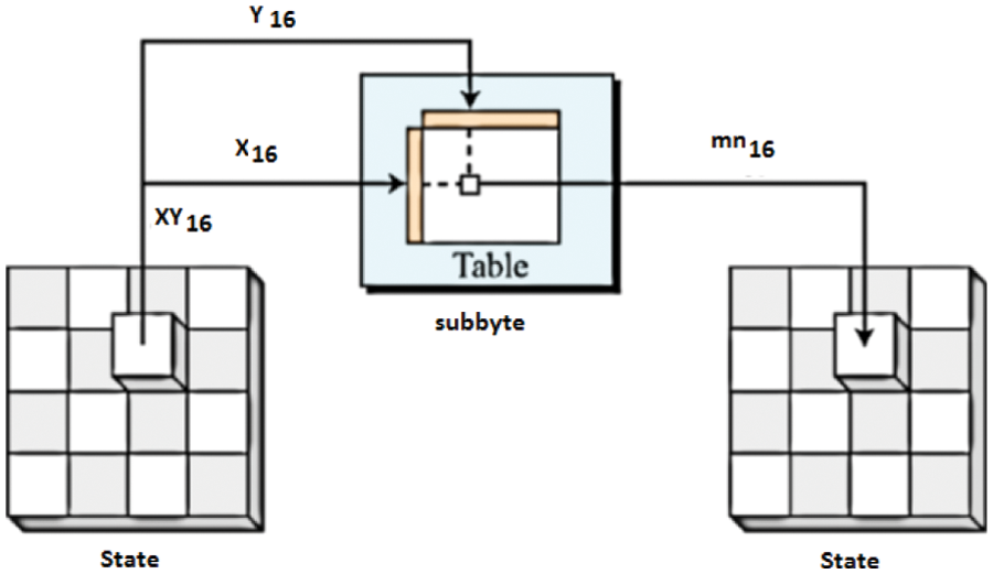
Figure 6: Subbyte transformation [36]
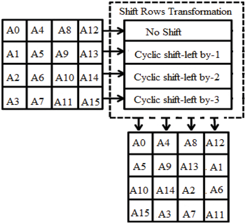
Figure 7: Row transformation
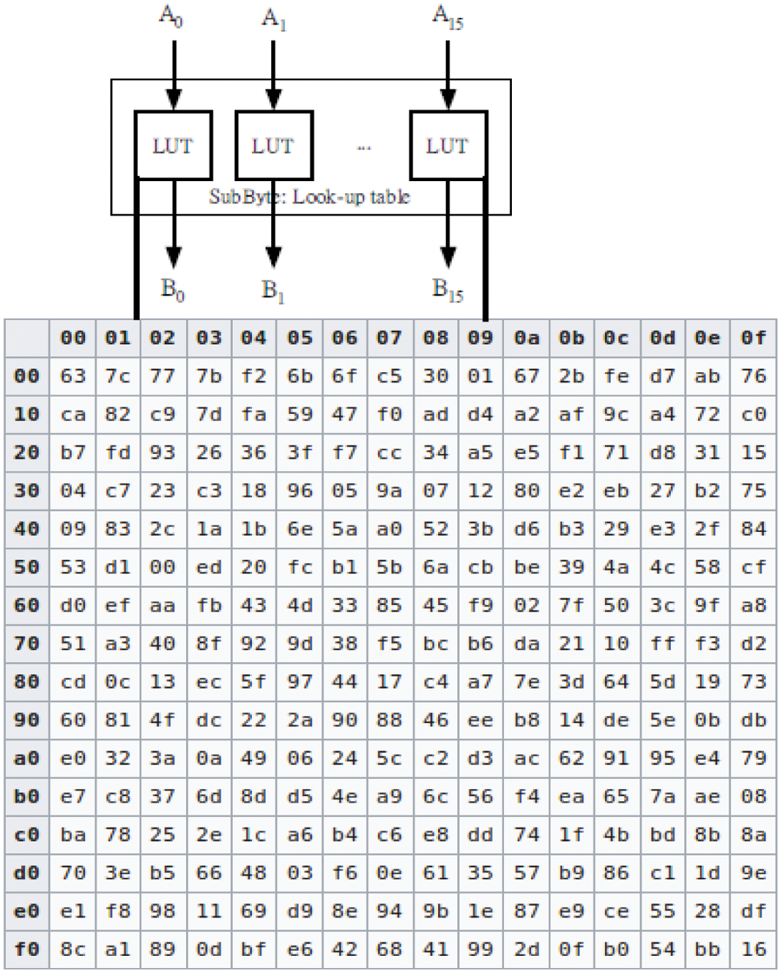
Figure 8: LUT with matrix [39]
The main prerequisite of AES is a high data rate. A high data rate is possible to achieve using pipelined structure. Pipelining is not mandatory for complete rounds in encryption/decryption, but one foremost limitation is that pipelining is only likely to be followed within each round. The next rounding operation is possible only when the previous rounding operation is completed. The best suitable design and architecture provide the best tradeoff between system clock frequency and Silicon space for larger throughput.
The S-box [38] transformation-based AES algorithm follows at least 16 clock cycles to complete the process of 16 elements over the S-box, and it is expected to complete the operation in one cycle for one element. There are four phases to each AES circular operation. The pipelined architecture provides the scalability and completion structures inside each circular. The total number of cycles required for 10 rounds is roughly 220 cycles, with an AES encryption procedure for 128-bit block data and a 128-bit key size. The chip silicon area can be reduced in this fashion, but good data throughput is sacrificed. In the exciting stage, the complete 10 rounds can be accomplished within 44 cycles and corresponding LUTs using the 16 S-box technique. High throughput is accomplished in this manner, even though a substantial silicon area is lost. As a result, the algorithm must be designed to maintain a balance between data flow and FPGA silicon area by incorporating four S-boxes (LUT). The encryption and decryption procedure takes 90 clock cycles to complete.
4 S-Box Encryptor/Decryptor Architecture
Fig. 9 depicts the overall pipelined architecture for the AES algorithm encryptor. The primary finite state machine (FSM) controller is linked to one register bank, multiplexer, S-box, latched pipelined register, mixed column module, key expander, and add the round key component, all of which are part of the same controller architecture. The user must provide the plain text to be transferred or encrypted in American Standard Code for Information Interchange (ASCII) format, as well as the password to decrypt the encrypted ciphertext back to the original plain text. As the user enters the key and plain text, the password expander component increases the initial password supplied to it, making it more suitable for all rounds of encryption algorithms. The encryption procedure begins after the key expansion phase is done. XOR operation is used to do a pre-round procedure with the actual 128-bit input data and key value, and the corresponding bit values are stored in register banks. The incomplete and remaining rounds of operation are finished as the pre-round operation is completed. These circular operations are completed in the following manner. The read data from the transitional register bank is used for four 32-bit multiplexers (4 × 1), and multiplexer logic select-based data is delivered to the input of the S-box module. The S-box transforms the data into consistent modified data and allows it to be combined with the column phase for further processing [40]. The 32-bit data is provided by the mix column step, which is progressed with an average matrix based on the method to give a 32-bit output. The result is now sent to the add round key module, which also has the password memory for 32-bit input data. Both inputs of two 32-bit are logically XORed with the help of this module and are their result is stored in the proceeding register bank further for the subsequent round. Therefore, the pipelined architecture provides the platform in which all these four columns of the original proceeding matrix are achieved one afterward and others are keeping all the components of the design fully busy. In the preceding round, the mix column level work is skipped and the obtained values from the add round key are saved from the output of the ciphertext memory.
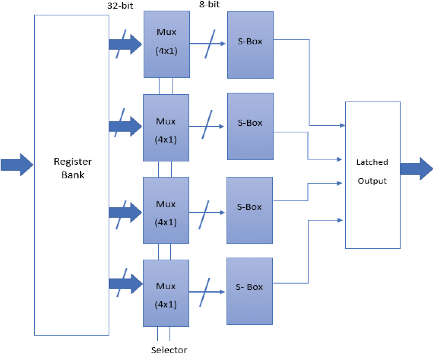
Figure 9: AES encryption architecture [40]
The FSM controller assists in the appropriate collection of the component and datapath for the round. The controller module directs the key module's scheduling in such a way that the keys advance for the round. The encryption procedure is completed in 88 cycles for 128-bit plain text or block and a 128-bit key, excluding the 62 cycles necessary for the key development and expansion module. It is also understood that the key expansion overhead is not becoming the cause of the degradation of the system performance because the same generated key is used again and again for the input of a larger size. The decryption module architecture is the reverse architecture of the encryption module. The best advantage of the pipelining stages is that it increases the throughput of the AES system and the multiplexer-based S-box matric implementation decreases the chip area without disturbing the throughput.
The hardware chip design and simulation are done in Xilinx ISE 14.7. The VHDL programming is used for the same. The register transfer level (RTL) of the designed chip is shown in Fig. 10. The RTL depicts the complete description of pins used in the chip configuration. The discussion of the pins is given in Tab. 1. The Xilinx integrated synthesis environment simulator (ISIM) simulator is used to verify the functional simulation for the grid data with 64-bit and 128-bit key sizes. Fig. 11 presents the simulation for 64-bit grid data and 64-bit key in binary and ASCII respectively. Figs. 12 and 13 presents the simulation for 128-bit grid data and 128-bit key in binary and ASCII respectively.
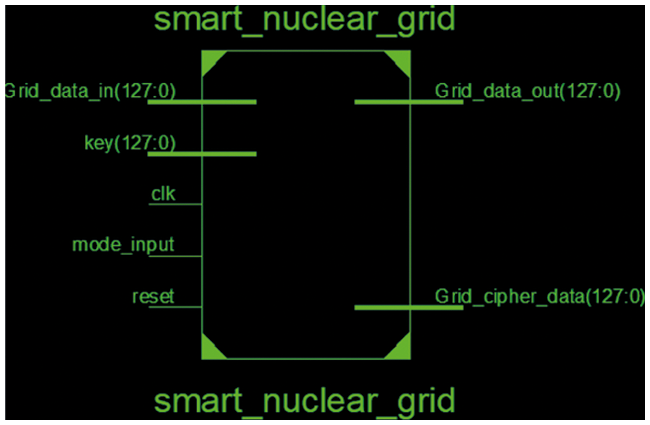
Figure 10: RTL view of the designed chip
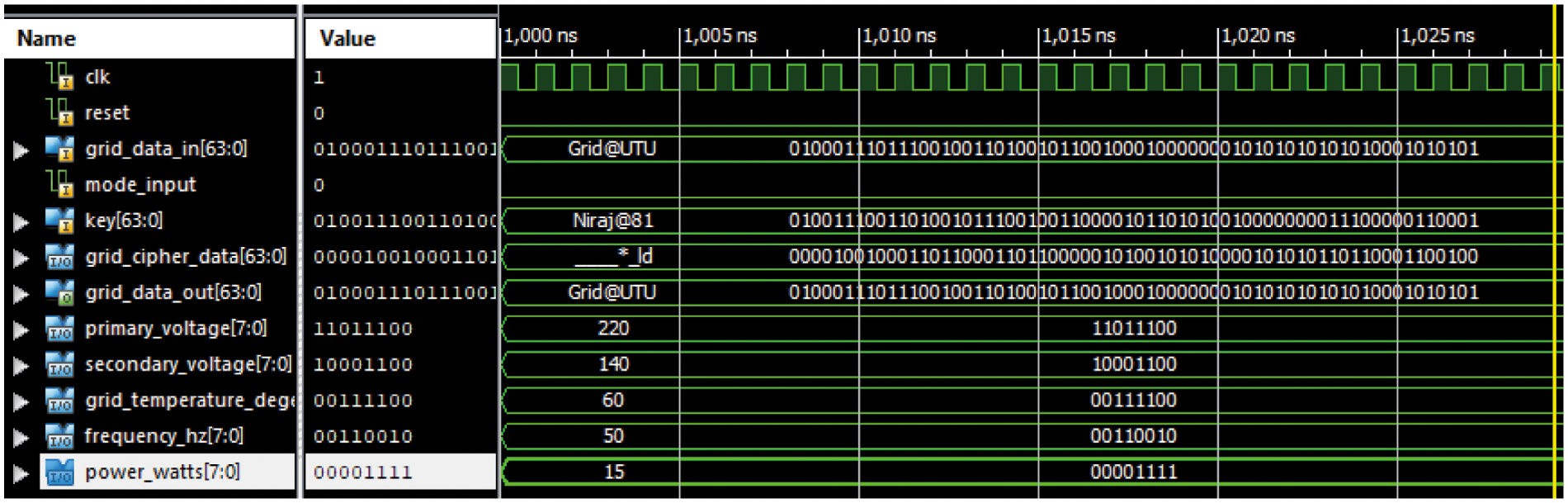
Figure 11: Xilinx ISIM simulation for key (64-bit) and grid data (64-bit) in binary and ASCII
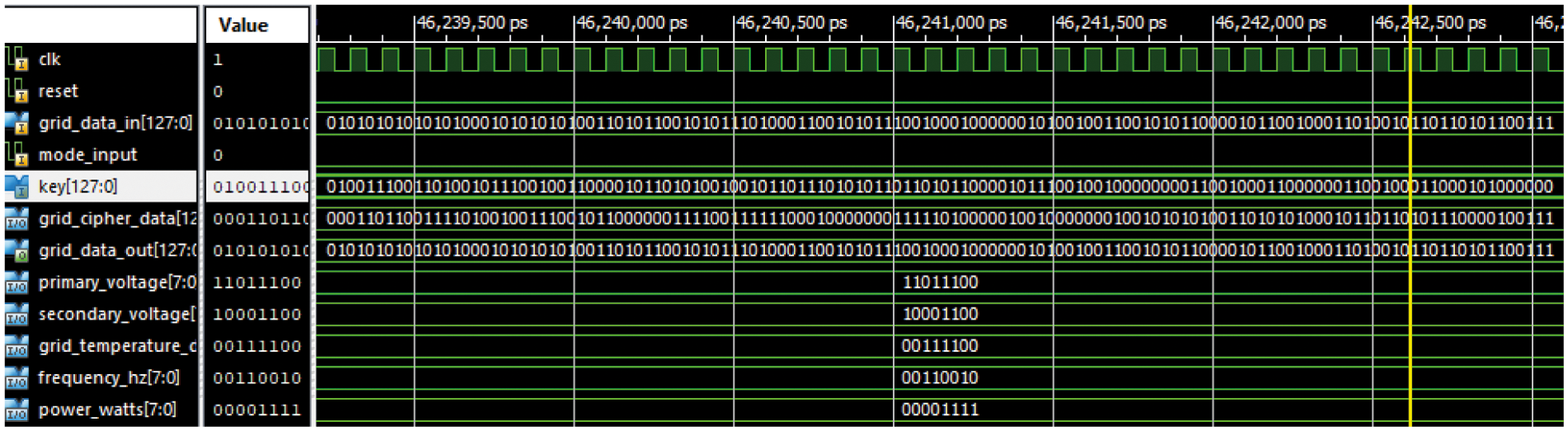
Figure 12: Xilinx ISIM simulation for key (128-bit) and grid data (128-bit) in binary
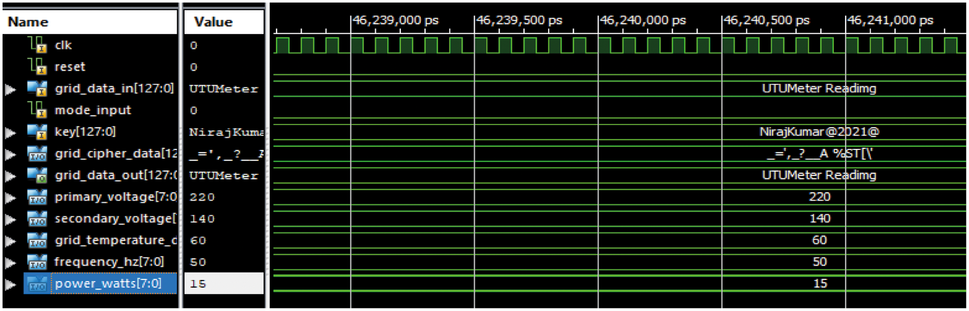
Figure 13: Xilinx ISIM simulation for key (128-bit) and grid data (128-bit) in ASCII
The chip design, waveform simulation, and FPGA synthesis are the main steps in the research methodology. The chip is followed using VHDL languages in the Xilinx software to see the RTL, inter schematic view, and view hardware synthesis report. The ISIM simulator from Xilinx is used to view the waveform using the integrated waveform simulator, which ensures that the chip is working. In the software environment, the test cases are simulated, and FPGA parameters are taken directly from the synthesis report. The tool includes all need to know about logic design, synthesis, simulation, verification, and timing analysis.
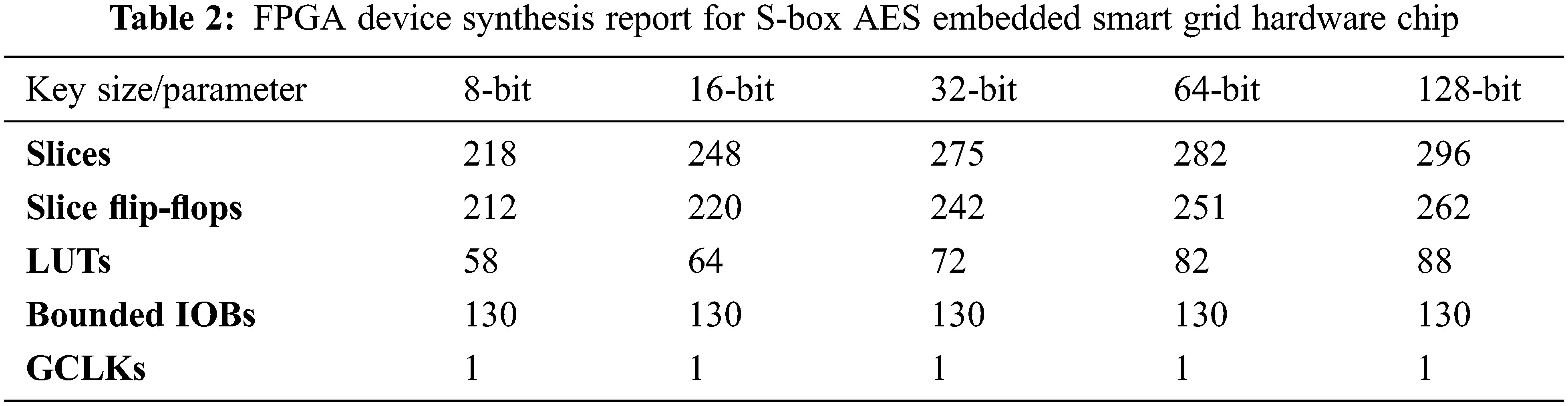
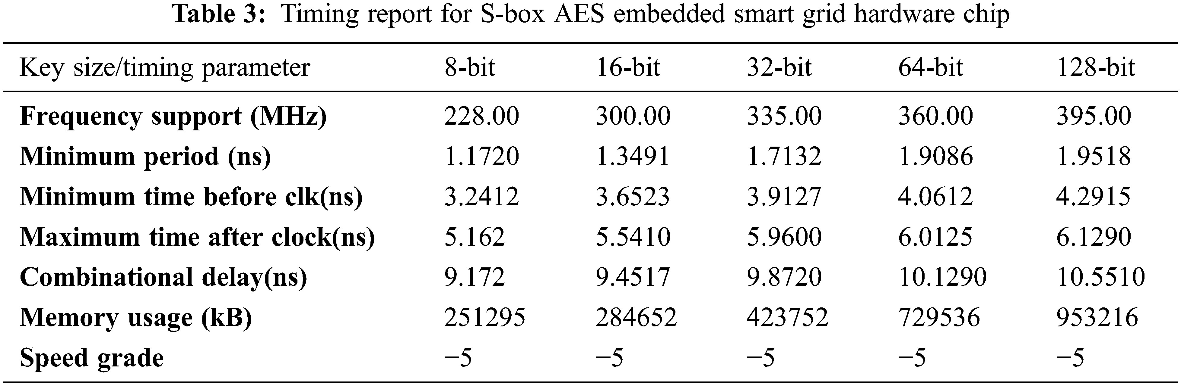
The Xilinx software-hardware utilization report is extracted that provides the hardware detail for the targeted FPGA device. The hardware parameters [41] are the number of slices, 4-input LUTs, bounded input/output block (IoB), flip-flops, global clock (GCLK), and chip memory (KB) utilized in the design. The timing report includes the detail of time parameters required for chip timing information [42] about minimum clock period (ns), minimum time (ns) necessary before the clock, maximum time (ns) after the clock signal, maximum frequency (MHz), and combinational path delay (ns) that include routing and logic delay [43]. The performance of the S-box AES is analyzed on the Vitex-5 FPGA hardware for these parameters. The synthesis parameters [44] are taken directly from the software [45]. Tabs. 2 and 3 present the detail of hardware usage and timing for the designed chip.
Figs. 14 and 15 show the graphs corresponding to the usage of hardware resources and timing-related metrics for various key sizes (8-bit, 16-bit, 32-bit, 64-bit, and 128-bit). The grid data is validated byte by byte on LEDs of the Virtex-5 FPGA. The simulation is carried at grid data assumptions: Primary voltage = 220 V, secondary voltage = 140 V, frequency = 50 Hz, grid temperature = 60°C, and Power = 15W are the grid characteristics used in the simulation.
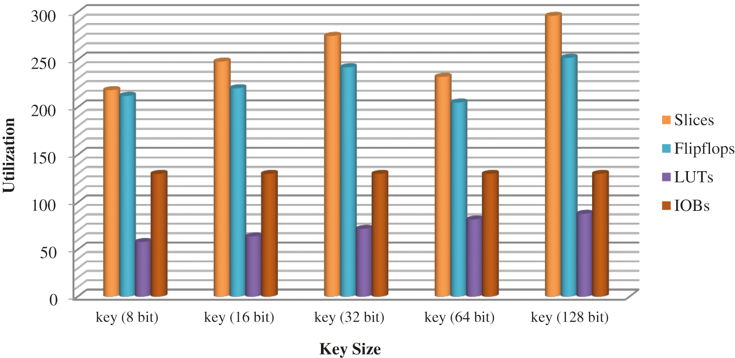
Figure 14: FPGA parameters as an overview of hardware
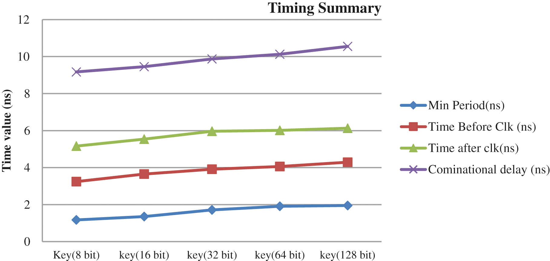
Figure 15: Utilization of timing-related parameters
The hardware simulation results predicted that the utilization is enhancing with the change in key size 8-bit to 128-bit and grid data. For 8-bit, 16-bit, 32-bit, 64-bit, and 128-bit, the slices utilization is 218, 248, 275, 282, and 296. In the same way, the timing parameters utilization is also increasing with the key size and grid data. The memory utilization is also increasing from 251295 to 953216 kB for 8-bit to the 128-bit key value. The FPGA synthesis results show that the designed chip is applicable for smart communication and faster switching in the grid.
Smart grids are built on new technology such as the internet of things (IoT) and artificial intelligence (AI), in which computers and gadgets are connected over the internet and work dynamically to share data, collect information, and improve automated processes and operational efficiency. In real-time, SCADA systems follow different communication protocols. The SCADA system is beneficial to facilities and industries that rely on control. The grid data is processed by the automated subsystem, which accepts commands. The smart grid cybersecurity hardware should handle potential risks from disgruntled employees, intelligence operations, and terrorists, as well as software failure vulnerabilities. The hardware chip integration of the S-box AES algorithm was successfully designed utilizing smart grid processing data, and communication was validated on the FPGA-Virtex-5. The main contribution is to design the S-Box AES hardware chip that can be embedded for grid security in real-time and the chip performance is studied based on FPGA hardware with the different key sizes and grid data (8-bit) to (128-bit). The grid supports the frequency of 395 MHz for 128-bit data communication integrated with AES. The most significant benefit of S-Box AES is that it can be implemented in both software and hardware. By inserting the developed chip in the grid communication system, the security of the smart grid SCADA system can be improved. FPGA hardware can process grid data and offer a safe and secure communication infrastructure between the distribution system and the client, or vice versa. In the future, we can integrate the concept of data compression and video processing in real-time with a larger size of grid data and key with the real-time operating system.
Funding Statement: The authors received no specific funding for this study.
Conflicts of Interest: The authors declare that they have no conflicts of interest to report regarding the present study.
1. A. R. Metke and R. L. Ekl, “Security technology for smart grid networks,” IEEE Transactions on Smart Grid, vol. 1, no. 1, pp. 99–107, 2010. [Google Scholar]
2. G. Dileep, “A survey on smart grid technologies and applications,” Renewable Energy, vol. 146, pp. 2589–2625, 2020. [Google Scholar]
3. M. Ourahou, W. Ayrir, B. E. Hassouni and A. Haddi, “Review on smart grid control and reliability in presence of renewable energies: Challenges and prospects,” Mathematics and Computers in Simulation, vol. 167, pp. 19–31, 2020. [Google Scholar]
4. L. Chhaya, P. Sharma, G. Bhagwatikar and A. Kumar, “Wireless sensor network based smart grid communications: Cyber-attacks, intrusion detection system and topology control,” Electronics, vol. 6, no. 1, pp. 5–20, 2017. [Google Scholar]
5. Y. Kabalci, “A survey on smart metering and smart grid communication,” Renewable and Sustainable Energy Reviews, vol. 57, pp. 302–318, 2016. [Google Scholar]
6. L. Chhaya, P. Sharma, A. Kumar and G. Bhagwatikar, “Communication theories and protocols for smart grid hierarchical network,” Journal of Electrical and Electronics Engineering, vol. 10, no. 1, pp. 43–50, 2017. [Google Scholar]
7. L. Chhaya, P. Sharma, G. Bhagwatikar and A. Kumar, “Development of wireless data acquisition and control system for smart microgrid,” Advances in Smart Grid and Renewable Energy, vol. 435, pp. 667–673, 2018. [Google Scholar]
8. R. Ma, H. H. Chen, Y. R. Huang and W. Meng, “Smart grid communication: Its challenges and opportunities,” IEEE Transactions on Smart Grid, vol. 4, no. 1, pp. 36–46, 2013. [Google Scholar]
9. W. Wang and Z. Lu, “Cyber security in the smart grid: Survey and challenges,” Computer Networks, vol. 57, no. 5, pp. 1344–1371, 2013. [Google Scholar]
10. N. Kumar, V. M. Mishra and A. Kumar, “Smart grid and nuclear power plant security by integrating cryptographic hardware chip,” Nuclear Engineering and Technology, vol. 53, no. 10, pp. 3327–334, 2021. [Google Scholar]
11. M. A. Ferrag, M. Babaghayou and M. A. Yazici, “Cyber security for fog-based smart grid SCADA systems: Solutions and challenges,” Journal of Information Security and Applications, vol. 52, pp. 102500, 2020. [Google Scholar]
12. K. Sayed and H. A. Gabbar, “SCADA and smart energy grid control automation,” Smart Energy Grid Engineering, vol. 1, pp. 481–514, 2017. [Google Scholar]
13. H. Kim, M. G. Na and G. Heo, “Application of monitoring, diagnosis, and prognosis in thermal performance analysis for nuclear power plants,” Nuclear Engineering and Technology, vol. 46, no. 6, pp. 737–752, 2014. [Google Scholar]
14. S. Katyara, M. A. Shah, B. S. Chowdhary, F. Akhtar and G. A. Lashari, “Monitoring, control and energy management of smart grid system via WSN technology through SCADA applications,” Wireless Personal Communications, vol. 106, no. 4, pp. 1951–1968, 2019. [Google Scholar]
15. L. Cardwell and A. Shebanow, “The efficacy and challenges of SCADA and smart grid integration,” Journal of Cyber Security and Information Systems, vol. 1, no. 3, pp. 1–7, 2016. [Google Scholar]
16. E. Brezhniev and O. Ivanchenko, “NPP smart grid mutual safety and cyber security assurance,” Cyber Security and Safety of Nuclear Power Plant Instrumentation and Control Systems, vol. 1, pp. 349–380, 2020. [Google Scholar]
17. A. Kovalenko, I. Babeshko, V. Tokarev and K. Leontiiev, “FPGA technology and platforms for NPP I&C systems,” Cyber Security and Safety of Nuclear Power Plant Instrumentation and Control Systems, vol. 1, pp. 419–457, 2020. [Google Scholar]
18. B. Peng, H. Xia, X. Ma, S. Zhu, Z. Wang et al., “A mixed intelligent condition monitoring method for nuclear power plant,” Annals of Nuclear Energy, vol. 140, pp. 107307–107310, 2020. [Google Scholar]
19. A. Kumar, K. Bansal, D. Kumar, A. Devrari, R. Kumar et al., “FPGA application for wireless monitoring in power plant,” Nuclear Engineering and Technology, vol. 53, no. 4, pp. 1167–1175, 2020. [Google Scholar]
20. K. Mahmood, S. A. Chaudhry, H. Naqvi, S. Kumari, X. Li et al., “An elliptic curve cryptography based lightweight authentication scheme for smart grid communication,” Future Generation Computer Systems, vol. 81, pp. 557–565, 2018. [Google Scholar]
21. S. Eom and J. H. Huh, “Group signature with restrictive linkability: Minimizing privacy exposure in ubiquitous environment,” Journal of Ambient Intelligence and Humanized Computing, pp. 1–11, 2018. [Google Scholar]
22. S. Eom and J. H. Huh, “The opening capability for security against privacy infringements in the smart grid environment.” Mathematics, vol. 6, no. 10, pp. 202–204, 2018. [Google Scholar]
23. O. G. Abood, M. A. Elsadd and S. K. Guirguis, “Investigation of cryptography algorithms used for security and privacy protection in smart grid,” in Proc. MEPCON, Cario, Egypt, pp. 644–649, 2017. [Google Scholar]
24. N. Kumar, V. M. Kumar and A. Kumar, “Smart grid security with AES hardware chip,” International Journal of Information Technology, vol. 12, no. 1, pp. 49–55, 2020. [Google Scholar]
25. A. Singh, A. Prasad and Y. Talwar, “Compact and secure S-box implementations of AES—A review,” Smart Systems and IoT: Innovations in Computing, vol. 141, pp. 857–871, 2020. [Google Scholar]
26. A. Kumar, P. Kuchhal and S. Singhal, “Secured network on chip (NoC) architecture and routing with modified TACIT cryptographic technique,” Procedia Computer Science, vol. 48, pp. 158–165, 2015. [Google Scholar]
27. A. Kumar, P. Vishnoi and S. L. Shimi, “Smart grid security with cryptographic chip integration,” EAI Endorsed Transactions on Energy Web, vol. 6, no. 23, pp. 1–12, 2019. [Google Scholar]
28. N. Ahmad, R. Hasan and W. M. Jubadi, “Design of AES S-box using combinational logic optimization,” in Proc. ISIEA, Penang, Malaysia, pp. 696–699, 2010. [Google Scholar]
29. C. Wang and H. M. Heys, “Using a pipelined S-box in compact AES hardware implementations,” in Proc. NEWCAS, Montreal, QC, Canada, pp. 101–104, 2010. [Google Scholar]
30. V. Rijmen and J. Daemen, “Advanced encryption standard. proceedings of federal information processing standards publications,” National Institute of Standards and Technology, vol. 14, no. 41, pp. 19–22, 2001. [Google Scholar]
31. W. Shuenn Shyang and N. Wan Sheng, “An efficient FPGA implementation of advanced encryption standard algorithm,” in Proc. ISCS, Vancouver, BC, Canada, pp. 2–597, 2004. [Google Scholar]
32. W. Stallings, “Cryptography and Network Security Principles and Practices,” 4th ed, vol. 1. New Delhi, India: Pearson Education, pp. 35–50, 2006. [Google Scholar]
33. S. Iyer, “Cyber security for smart grid, cryptography and privacy,” International Journal of Digital Multimedia Broadcasting, vol. 2011, no. 372020, pp. 1–8, 2011. [Google Scholar]
34. M. E. Hameed, M. M. Ibrahim and N. A. Manap, “Review on improvement of advanced encryption standard (AES) algorithm based on time execution, differential cryptanalysis and level of security,” Journal of Telecommunication, Electronic and Computer Engineering, vol. 10, no. 1, pp. 139–145, 2018. [Google Scholar]
35. A. Alhothaily, C. Hu, A. Alrawais, T. Song, X. Cheng et al., “A secure and practical authentication scheme using personal devices,” IEEE Access, vol. 5, pp. 11677–11687, 2017. [Google Scholar]
36. M. R. Rao and R. K. Sharma, “FPGA implementation of combined AES-128,” in Proc. ICCCNT, Delhi, India, pp. 1–6, 2017. [Google Scholar]
37. H. Prasad, J. Kandpal, D. Sharma and G. Verma, “Design of low power and secure implementation of S-box for AES,” in Proc. INDIACOM, New Delhi, India, pp. 2092–2097, 2016. [Google Scholar]
38. S. Morioka and A. Satoh, “A 10-gbps full-AES crypto design with a twisted BDD S-box architecture,” IEEE Transactions on Very Large-Scale Integration (VLSI) Systems, vol. 12, no. 7, pp. 686–691, 2004. [Google Scholar]
39. P. Zhang, O. Elkeelany and L. McDaniel, “An implementation of ecured smart grid ethernet communications using AES,” in Proc. Southeast Con, Concord, NC, USA, pp. 394–397, 2010. [Google Scholar]
40. S. S. Priya, P. Karthigaikumar, N. S. Mangai and P. K. G. Das, “An efficient hardware architecture for high throughput AES encryptor using MUX-based sub pipelined S-box,” Wireless Personal Communications, vol. 94, no. 4, pp. 2259–2273, 2017. [Google Scholar]
41. H. Zodpe and A. Sapkal, “An efficient AES implementation using FPGA with enhanced security features,” Journal of King Saud University-Engineering Sciences, vol. 32, no. 2, pp. 115–122, 2020. [Google Scholar]
42. A. Kumar, G. Verma, M. K. Gupta, M. Salauddin, B. K. Rehman et al., “3D multilayer mesh NoC communication and FPGA synthesis,” Wireless Personal Communications, vol. 106, no. 4, pp. 1855–1873, 2019. [Google Scholar]
43. A. Kumar, L. Baruha and A. Sabu, “Rotator on-chip (RoC) design based on ring topological NoC,” Procedia Computer Science, vol. 45, pp. 540–548, 2015. [Google Scholar]
44. A. Jain, R. Dwivedi, A. Kumar and S. Sharma, “Scalable design and synthesis of 3D mesh network on chip,” Advances in Intelligent Systems and Computing, vol. 479, pp. 661–666, 2017. [Google Scholar]
45. A. Jain, A. Kumar and S. Sharma, “Comparative design and analysis of mesh, torus and ring NoC,” Procedia Computer Science, vol. 48, pp. 330–337, 2015. [Google Scholar]
 | This work is licensed under a Creative Commons Attribution 4.0 International License, which permits unrestricted use, distribution, and reproduction in any medium, provided the original work is properly cited. |