DOI:10.32604/iasc.2022.020552
| Intelligent Automation & Soft Computing DOI:10.32604/iasc.2022.020552 | |
| Article |
Design of Higher Order Matched FIR Filter Using Odd and Even Phase Process
1Department of Electronics and Communication Engineering, Velammal Engineering College, Chennai, 600066, India
2Department of Computer Science and Engineering, Velammal Engineering College, Chennai, 600066, India
*Corresponding Author: V. Magesh. Email: magesh@velammal.edu.in
Received: 29 May 2021; Accepted: 11 July 2021
Abstract: The current research paper discusses the implementation of higher order-matched filter design using odd and even phase processes for efficient area and time delay reduction. Matched filters are widely used tools in the recognition of specified task. When higher order taps are implemented upon the transposed form of matched filters, it can enhance the image recognition application and its performance in terms of identification and accuracy. The proposed method i.e., odd and even phases’ process of FIR filter can reduce the number of multipliers and adders, used in existing system. The main advantage of using higher order tap-matched filter is that it can reduce the area required, owing to its odd and even processes. Further, it also successfully reduces the time delay, especially in case of high order demands. The performance of higher order matched filter design, using odd and even phase process, was analyzed using Xilinx 9.1 ISE Simulator. The study results accomplished reduction in area, 70% increase in throughput compared to traditional implementation and reduced time delay. In addition to these, Vedic multiplier-based FIR is modified with a tree-based MAM that reduces the number of shifter and adder to replace the multiplier.
Keywords: Area-efficient; matched filter; high order; image recognition
Finite Impulse Response (FIR) filter is one of the digital filters used to build Digital Signal Processing (DSP) [1] hardware. FIR digital filters are stable and possess linear phase properties due to which it is commonly applied in numerous electronic systems over a wide range of applications such as audio and video signal processing, channel equalization, data compression, matched filtering, digital audio and video recording, and pulse shaping [2]. Digital filters are widely used in present day DSP. Both speed and power optimization play a quality factor in FIR filter, due to high performance in DSP applications. The need for tradeoff between power consumption [3] and speed in DSP applications can be easily fulfilled with the help of digital filter circuits. Nowadays, Field Programmable Gate Arrays (FPGAs) act as a platform for digital VLSI (Very Large Scale Integration) designs. FPGAs possess few key characteristics like high flexibility, reusability, low power, moderate cost, easy upgradation and feature extension facilities. It provides an array of adjustable logic modules that are interconnected with programmable routing resources and encircled by programmable input/output blocks. The authors, in current study, presents the design and implementation of higher order-matched filter using odd and even phase processes of FIR filter for image recognition applications based on performance analysis. In recent times, image recognition applications [4,5] are widely used in daily life and it has gained popularity in numerous domains such as video stream display, person or object identification, biomedical/ultrasound image-assisted diagnosis and under-water exploration tasks. Matched filters [6,7] are widely used tools in the recognition of a specified part. The implementation of higher-order taps on transposed form of the matched filters [8] can enhance image recognition applications and its performance in terms of identification and accuracy. But, it results in large design area implementation in hardware system. Thus, in order to overcome the difficulties in existing systems, an area-efficient VLSI design of higher order-matched filter is proposed with the help of odd and even phase processes of FIR filter. Rest of the sections in this paper are organized as given herewith. Section 2 reviews the proposed area-efficient VLSI architecture. Design implementation of ripple carry adder, Vedic multiplier, D-Flip-flop and multiplexers are presented in Section 3. Section 4 discusses the results obtained using Xilinx and Modelsim whereas Section 5 concludes the paper.
2 Proposed Area-Efficient VLSI Architecture
In order to realize the operation of matched filter in DSP applications, it should be implemented based on typical transposed form circuit [8], as an 8-tap example shown in Fig. 1. It is an established fact that direct form implementation results in lower area and low power dissipation. Though the transposed form offers high speed, yet it requires larger area. In this scheme, the critical path consists of ‘multiplication’ and ‘add’ operations during every stage. The filter’s latency gets reduced because the final-carry propagation is not needed beyond the last stage. This further increases the area and power dissipation in filters. But, it is disadvantageous that N multipliers and (N-1) adders are required. As the value of N increases, the need for components also gets increased. Therefore, the proposed area-efficient matched filter design of FIR filter enables the users to determine the matched filter configuration in a flexible manner.

Figure 1: Hardware design of 8-tap typical transposed form circuit
Fig. 2 shows the proposed FIR filter with 8-tap design of higher order-matched filter using odd and even phase process as example. A control signal (C) is defined as a one-bit counter to toggle between every clock cycle. The entire set of clock cycles is divided into two phases namely, odd and even-indexed phases i.e., C = 1 and C = 0, respectively. If C = 0, the system performs all the multiplication-and-additional processing with even-indexed phase coefficient taps (W0, W2, …) and stores the value at memory storage i.e., Even-Phase Result (EPR). On the other hand, if C = 1, the system performs all the multiplication-and-addition processing with odd-indexed phase coefficient taps (W1, W3, …) and stores the value at memory storage i.e., Odd-Phase Result (OPR). The addition of even-phase results and odd-phase results yields the results for every clock cycle.
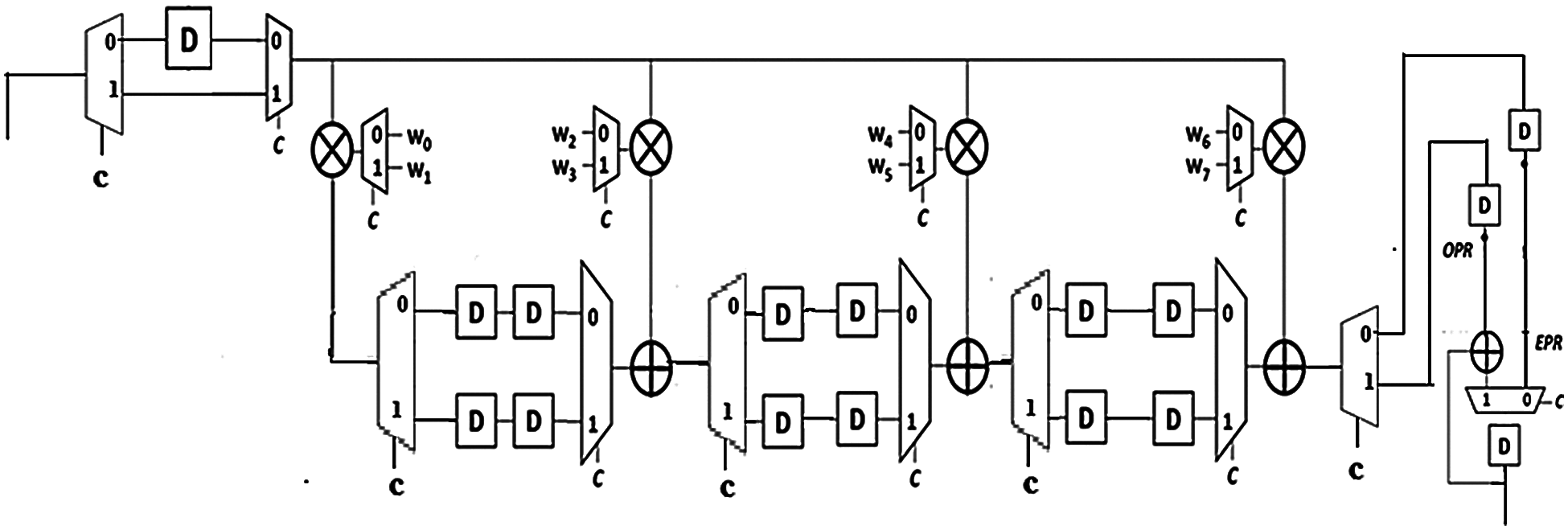
Figure 2: Hardware design of 8-tap proposed FIR filter using odd and even phase process
Full adder is a widely used circuit that performs the addition of three bits. A one-bit full adder consists of three inputs (such as a, b, and cin) as illustrated in Fig. 3. The truth table of a full adder is tabulated in Tab. 1. The gate implementation of 1-bit full adder is shown in Fig. 4.
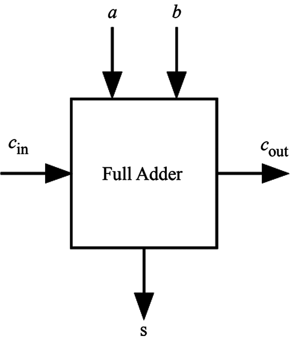
Figure 3: One bit full adder

Figure 4: Gate implementation of full adder
Ripple carry adder is a digital circuit that performs the addition of binary numbers and yields the output. It is designed as a combination of full adders connected in series in which the output is fed as next input. Fig. 5 shows the design implementation of 4-bit ripple carry adder which is made up of four full adders. It is to be noted in Fig. 5 that the inputs of 4-bit ripple carry adder are a0-a4 and b0-b4 which represent the Least Significant Bit (LSB).

Figure 5: 4-bit ripple carry adder

The multiplication operation is performed by a simple Vedic multiplier architecture on the basis of Urdhva-Triyakbhyam. This method performs the multiplication operation in both vertical and crosswise directions, called as sutra. Sutra is a traditional method, used in ancient India, for multiplication purpose. In Urdhva Tiryagbhyam sutra, the multiplication is done in vertical and cross-wise operations. The 2 × 2 Vedic multiplier performs the multiplication operation as briefed in the following steps.
Stage 1: The prior, least significant bit of two binary numbers is to be multiplied vertically and these numbers are also summed up with previous carry over i.e., zero in this case. LSB bit is considered as the result in output bits whereas the remaining bits are forwarded to next stage.
Stage 2: In this stage, two binary bits are cross-multiplied and the results are added to the previously-generated carry. Again, the LSB bit of the output bits is considered as the result whereas the remaining bits are forwarded to next stage.
Step 3: In this stage, the most significant bits are multiplied vertically. The resultant values are then added to the previously-generated carry after which the output is taken as the result. An example for Vedic multiplication is shown in Fig. 6.
The block diagram of 2X2 Vedic multiplier is shown in Fig. 7. Fig. 8 shows the 2X2 Vedic multiplier in which four AND gates and TWO Half adder circuits are used in current research work. Fig. 9 depicts the implementation of MCM block without using the proposed algorithm. The expected output would be 4 bits whereas the inputs for this multiplier will be in the form of pulses.
Following is the list of steps followed in Vedic multiplication.
Step 1: Multiply the two digits of input on the right side
Step 2: Cross multiply the input digits of both columns and add together
Step 3: Multiply the two digits of input on the left side
Example: 21 × 32
Step 1: 1 × 2 = 2; write 2 for right column
Step 2: 2 × 2 = 4
Step 3: 3 × 1 = 3; add 3 + 4 = 7, for middle column
Step 4: 2 × 3 = 6; write 6 for left column

Figure 6: 2X2 vedic multiplication

Figure 7: Block diagram of 2X2 vedic multiplier
Fig. 8 shows the hardware detail for the multiplier in which “a” and “b” are two numbers to be multiplied while “q” denotes the product. The design is represented in verilog code in the form of gates and half adders.

Figure 8: Hardware implementation of 2X2 vedic multiplier
The final result is c2s2s1s0. Eqs. (1)–(3) represent the results of 2X2 Vedic multiplier.
4 Proposed Algorithm for the Implementation of MCM Block
The current research work proposes a Multiple Constant Multiplication (MCM)-based FIR filter algorithm design with an aim to find a coefficient set that can be synthesized into an adder-and-shift network with the least number of shifters and Average Adder Depth (AAD) of SAs. The tree search-based proposed method traverse along a specific path in order to realize the coefficients with least number of shifters and adders. A decline in the number of shifters and adders eventually leads to reduction in chip area. Generally, the adder cost of SAs is determined by fixed filter order. So, the lower AAD also leads to lower power consumption of SAs. In conventional model [9–16], each and every discrete coefficient of FIR filter is implemented using shifters and adders networks individually. There is no connection between adder and shifter network of any two coefficients. So, no adder or shifter is used commonly during the implementation of any two coefficients of shifter and adder. In the proposed model of MCM block implementation, both shifters and adders are shared among numerous coefficient implementations. This is made possible by applying the proposed algorithm to find the root node, which is realized with the help of adder and shifter networks and its output value is shared among the eligible coefficients’ hardware implementation. Figs. 10 and 11 provide a clear idea about the difference between conventional model and the proposed model of MCM block design.

Figure 9: Implementation of MCM block without using the proposed algorithm (conventional method)

Figure 10: Implementation of MCM block using the proposed algorithm
The algorithm used to find the definite path consists of intermediate nodes. These intermediate nodes are nothing but quantized coefficients for computing each coefficient from the given set of discrete fixed coefficient set of N-order FIR filter.
In order to design a multiple constant multiplication block of FIR filter, a root node is generated from the given set of fixed discrete coefficients under some conditions. This results in the production of child nodes from which other root nodes get generated. This process gets repeated until all the coefficients are computed in the optimized path that require minimum number of shifters and adders. A detailed procedure for the proposed algorithm is given below:
1. First, the discrete coefficients of N-order FIR filter, which are already quantized to discrete coefficient set, within the required word length from continuous coefficient set in descending order, are sorted.
2. Out of the sorted coefficient list, the coefficients that are powers of 2 are not considered for further computation. They are removed from coefficient list, since they can be implemented only with the help of left shifter without any need for adders.
3. To find the discrete root node, the bit position with maximum number of 1’s from Maximum Significant Bit (MSB) is to be checked against the bit position before LSB in the list of binary representation of discrete coefficients. If two or more bit positions has the same count of logic 1 and remains the maximum count, then the position nearby the MSB is selected.
4. Consider the smallest coefficient, among the coefficients, with selected bit position that has the maximum number of logic 1.
5. In the smallest coefficient considered, the bits from the selected bit are considered from position up to the LSB of that coefficient. This forms the root node.
6. Subtract the root node value from all other coefficients greater than or equal to root value. The result obtained, out of subtraction, forms the child nodes. Then, append this value to pathlist of coefficients, greater than equal to root node, where pathlist is the list of optimum paths for each and every coefficient of N-order FIR filter.
7. Once again, a root node is computed by following the procedure discussed above, for the set of generated child nodes. The root nodes generated at each level are stored in a list. Because, if the same root node is generated after some steps, the existing root nodes can be reused which in turn further reduces the number of shifters and adders.
8. If the child node is a ‘power of two’ number, then it can be directly obtained by means of shifters. Thus, they are not included in further calculation process by are added to the pathlist of that specific coefficient.
9. Further, if any child node computed is equal to root node value generated earlier, then the child node is not considered for further calculation, because the already-implemented root node can be reused.
10. If two child nodes are left, then the smaller child node is considered as the root node and step 6 is repeated.
11. The above steps are repeated until a single child node is left. The final left-out child node is added to the pathlist of particular coefficient.
The proposed higher order-matched filter, using odd and even phase process, was designed using verilog programming. This module was used in the construction of FIR filter using Verilog programming. The functionality of FIR filter was verified using Modelsim simulator. Fig. 11 shows the simulation result. The proposed system was synthesized using Xillinx ISE tool for FPGA Spartan 6. Fig. 12 shows the Register Transfer Logic (RTL) view for the proposed system whereas Fig. 13 shows a detailed view of RTL for the proposed system. Tab. 2 provides a summary on device utilization obtained, while performing the experiment in Xilinx 3s250eft256-4.

Figure 11: Simulation result of the proposed system

Figure 12: RTL view of the proposed system

Figure 13: Detailed RTL view of the proposed vedic multiplier FIR system


Figure 14: Detailed RTL view of the proposed vedic multiplier FIR system
Tab. 3 compares the existing and proposed methods under different measures. Tab. 3 infers that the proposed model showed a drastic decline in delay time. The existing system had a delay of 18.189 ns whereas the proposed system had a delay of 10.330 ns. This delay was obtained only by the addition of registers with existing model. The number of slices, used by both existing and proposed are more or less the same. Fig. 14 compares the number of adders and shifters used by conventional and the proposed MCM FIR filters.

The number of IOs used by existing and the proposed models remains the same. Therefore, high throughputs were achieved without bringing much change in the model. Fig. 15 shows the involvement of different techniques in FIR filter and the number of slices, Look Up Tables (LUTs), Flip-Flops, IOs and delay used in the FIR filter.

Figure 15: Comparisons of various techniques
The current research paper proposed to design a higher order-matched filter using odd and even phase processes through Vedic multiplier in order to achieve low power and fixed structure and due to less usage of comparators and simple logic in this multiplier. MCM-based FIR filter offers low area. A further improvement is highly effective, owing to its low delay and high throughput. From the experimental results, it is inferred that the existing model produces low throughput at less speed. While the modified model, with same hardware and addition of registers, reduced the time delay in the existing system. With regards to matched filter design, utilized in image recognition applications, the current study implemented an area-efficient VLSI hardware architecture in a system that requires high-order taps. By using odd-phase and even-phase calculation operations, one can save circuit components including multipliers and adders from getting utilized. The proposed model totally saves the design area in comparison with typical transposed form circuit. The proposed MCM-based FIR filter was implemented using a modified algorithm. The result confirmed that the area, in terms of slices, was lesser than the Vedic implementation. The proposed Vedic-based FIR Filter was implemented and the results show that there was a decline in delay from 18.189 to 10.330 ns which in turn increased the speed of operation from 54 to 96 MHz.
Funding Statement: The authors received no specific funding for this study.
Conflicts of Interest: The authors declare that they have no conflicts of interest to report regarding the present study.
1. A. P. Vinod and E. Lai, “Low power and high speed implementation of FIR filters for software define radio receivers,” IEEE Transactions on Wireless Communications, vol. 5, no. 7, pp. 1669–1675, 2006. [Google Scholar]
2. B. Sakthivel and A. Padm, “Area and delay efficient GDI based accuracy configurable adder design,” Microprocessors and Microsystems, vol. 73, pp. 102958, 2020. [Google Scholar]
3. X. Y. Shih, Y. Q. Liu and Y. T. Cheng, “Area-efficient VLSI architecture of high-order matched filter design using odd-and-even phase processing for image recognition applications,” in 2018 IEEE Int. Conf. on Consumer Electronics-Taiwan, Taichung, Taiwanm, IEEE, pp. 1–2, 2018. [Google Scholar]
4. Y. Liang, P. P. Markopoulos and E. S. Saber, “Subpixel target detection in hyperspectral images with local matched filtering in SLIC superpixels,” in 2016 8th Workshop on Hyperspectral Image and Signal Processing: Evolution in Remote Sensing, Los Angeles, CA, USA, pp. 1–5, 2016. [Google Scholar]
5. S. Buganim and S. R. Rotman, Matched Filters for Multispectral Point Target Detection, San Diego, California, United States, pp. 63020Z, 2006. [Google Scholar]
6. J. G. Proakis and D. G. Manolakis, Digital Signal Processing, 4th ed., Upper Saddle River, N.J: Pearson Prentice Hall, 2007. [Google Scholar]
7. S. Ariprasath and C. Santhi, “Transpose form FIR filter design for fixed and reconfigurable coefficients,” International Research Journal of Engineering and Technology, vol. 4, no. 3, pp. 53–78, 2017. [Google Scholar]
8. B. N. M. Kumar and R. H. Gangappa, “Low area VLSI implementation of CSLA for FIR filter design,” International Journal of Intelligent Engineering and Systems, vol. 12, no. 4, pp. 512–518, 2019. [Google Scholar]
9. V. S. Harshini and K. K. S. Kumar, “Design of hybrid sorting unit,” in 2019 Int. Conf. on Smart Structures and Systems, Chennai, India, pp. 1–6, 2019. [Google Scholar]
10. R. Seshasayanan and K. K. Senthil Kumar, “Reconfigurable architecture For WTLS,” in 2006 Annual IEEE India Conf., New Delhi, India, IEEE, pp. 1–4, 2006. [Google Scholar]
11. L. Aksoy, E. Costa, P. Flores and J. Monteiro, “Design of low-power multiple constant multiplications using low-complexity minimum depth operations,” in Proc. of the 21st Edition of the Great Lakes Sym. on Great Lakes Symp. on VLSI-GLSVLSI ’11, Lausanne, Switzerland, pp. 79, 2011. [Google Scholar]
12. B. Y. Kong and I. C. Park, “FIR filter synthesis based on interleaved processing of coefficient generation and multiplier-block synthesis,” IEEE Transactions on Computer-Aided Design of Integrated Circuits and Systems, vol. 31, no. 8, pp. 1169–1179, 2012. [Google Scholar]
13. A. Shahein, Q. Zhang, N. Lotze and Y. Manoli, “A novel hybrid monotonic local search algorithm for FIR filter coefficients optimization,” IEEE Transactions on Circuits and Systems I: Regular Papers, vol. 59, no. 3, pp. 616–627, 2012. [Google Scholar]
14. D. Shi and Y. J. Yu, “Design of linear phase FIR filters with high probability of achieving minimum number of adders,” IEEE Transactions on Circuits and Systems I: Regular Papers, vol. 58, no. 1, pp. 126–136, 2011. [Google Scholar]
15. W. B. Ye and Y. J. Yu, “Switching activity analysis and power estimation for multiple constant multiplier block of FIR filters,” in 2011 IEEE Int. Sym. of Circuits and Systems, Rio de Janeiro, Brazil, pp. 145–148, 2011. [Google Scholar]
16. W. B. Ye and Y. J. Yu, “Single-stage and cascade design of high order multiplierless linear phase FIR filters using genetic algorithm,” IEEE Transactions on Circuits and Systems I: Regular Papers, vol. 60, no. 11, pp. 2987–2997, 2013. [Google Scholar]
 | This work is licensed under a Creative Commons Attribution 4.0 International License, which permits unrestricted use, distribution, and reproduction in any medium, provided the original work is properly cited. |