| Fluid Dynamics & Materials Processing |
DOI: 10.32604/fdmp.2022.019132
ARTICLE
Optimization of the Thermoelectric Performances of CoSbS Semiconductors Using the High-Pressure Fabrication Method
1Wuhan Technology and Business University, Wuhan, 430065, China
2South Central University for Nationalities, Wuhan, 430074, China
*Corresponding Author: Min Wang. Email: liufang882@163.com
Received: 04 September 2021; Accepted: 21 November 2021
Abstract: CoSbS-based compounds are good thermoelectric materials with low thermal conductivity and good electrical properties, which can effectively be used to improve the efficiency of many thermoelectric conversion processes. In order to improve their properties even more, in this study a series of experiments have been conducted in the frame of the traditional solid-phase synthesis and high-pressure method. It is shown that if the mass fluctuation and stress fluctuation in the considered CoSbS system increase, the scattering probability of phonons is enhanced and the lattice thermal conductivity of the material is reduced. Adding a small amount of Se can simultaneously optimize three thermoelectric properties, i.e., the Seebeck coefficient is improved, the thermal conductivity becomes smaller and the quality factor grows. At the same time, the thermal and electrical properties of bulk materials can be optimized by using nano-scale Ni doped CoSbS samples. As shown by the experiments, Ni-doped Co sites can effectively improve the carrier concentration, the effective mass of the density of states of the material, and the power factor. Under the same temperature conditions, the thermoelectric figure of merit (ZT) of Co1−yNiySbS1−xSex synthesized under high pressure, at x = 0.15, y = 0.1 is much higher than the corresponding value for CoSbS prepared by traditional methods.
Keywords: High pressure preparation; micro-nano composite; thermoelectric merit; CoSbS
Thermoelectric conversion technology can realize the mutual conversion of heat energy and electric energy, and it is a new energy technology that can realize the mutual conversion of heat energy and electric energy in all solid state. The key factor of thermoelectric conversion technology is to find thermoelectric materials with high conversion efficiency. Thermoelectric materials are new energy materials that use Seebeck effect or Pielter effect to realize direct conversion between heat energy and electric energy. The development of semiconductor technology promotes the development of thermoelectric materials. CoSbS-based compound, namely parathiostibium cobalt ore, is a new type of mineral thermoelectric material with high Seebeck coefficient and narrow band gap (∼0.69 eV). CoSbS, a cobalt derivative, has good stability, good mechanical properties, easy preparation, low price of elements, innocuity, abundant reserves of constituent elements and so on, which has broad prospects in application fields. Among semiconductor materials, materials with a band gap of less than 1 eV have the potential to be used as thermoelectric materials. The Seebeck coefficient of CoSbS-based compound ranges from 250 μV/K to 400 μV/K. Compared with known thermoelectric materials with excellent performance, CoSbS has excellent thermoelectric properties.
The intrinsically undoped CoSbS sample of CoSbS-based compound has a low carrier concentration (1017 cm−3) and a high thermal conductivity (∼9.36 W·m−1·K−1). At 900 K, its ZT value is only 0.19, which is serious this limits the large-scale application of CoSbS-based thermoelectric materials. Therefore, it is urgent to optimize the conductivity and thermal conductivity of the material to improve its thermoelectric properties. In this paper, X-ray single crystal diffraction of Fukou Iron Mine is studied. The mineral belongs to orthorhombic system. In this paper, the crystal structure is obtained by Patterson function analysis and electron density distribution function, and the atomic coordinates are modified by least square method and optimization method. The basic structural unit is a double octahedron composed of two cobalt-antimony and sulfur octahedrons with S-S common edges, which are connected by vertices [1,2]. And Sb and s are connected with 3-pair [SbS] through covelent bond, Through crystal analysis, it is clear that the structure of the auxiliary stone is the same as that of the auxiliary stone [3]. The crystal structure is shown in Fig. 1.

Figure 1: The crystal structure of CoSbS
In 1821, Seebeck, a German scientist, discovered that in a loop composed of two different conductive materials, when the two contacts are at different temperatures T1 and T2, there will be a voltage difference (electromotive force) between the two contacts, thus generating a current in this loop. The voltage difference (electromotive force) that produces this current is called thermoelectromotive force, and this phenomenon is later called the Seebeck effect [4–6]. Based on this effect, thermoelectricity can be converted into electrical energy, that is, two different conductors or semiconductors A and B are combined into a closed loop as shown in the figure. If the temperature at the junction of conductors A and B is different (set T > T0), then there will be current in the closed loop, that is to say, there is electromotive force in the loop. This phenomenon is called thermoelectric effect. The thermoelectric potential is composed of two parts, the thermoelectric potential and contact potential. The closed circuit composed of conductor materials A and B has the junction temperature of T and T0, respectively. If T > T0, there must be two contact potentials and two temperature difference potentials. According to the principle, the equation of total circuit potential is Eq. (1).
The Seebeck coefficient SA is the voltage difference divided by the temperature difference, which is Eq. (2).
When the material is an n-type semiconductor, the Seebeck coefficient of the n-type semiconductor material is negative. When material A is an A P-type semiconductor, the situation is just the opposite. When two different metals or semiconductor materials are in contact, the difference of electron bulk density will be eliminated by the movement of internal carriers (electrons or holes) on the contact surface. The movement rate of electrons is related to the temperature of the contact area. In order to form a stable potential difference between two different materials, it is necessary to keep a temperature gradient between two materials, so as to ensure the continuous movement of electrons. At the same time, it should be noted that Seebeck effect is not an interface effect, but two different materials need to be contacted to measure it. When the carrier is an electron, an electric field that resists the temperature gradient will be generated, which leads to a negative Seebeck coefficient. On the contrary, when the carrier is a hole, the Seebeck coefficient is a positive value. Seebeck coefficient can characterize the intensity of Seebeck effect. When the temperature difference is constant, the greater the potential difference between the two ends of the device, the greater the Seebeck coefficient will be. The Seebeck coefficient of p-type semiconductor is positive, while that of n-type semiconductor is negative. The international unit of Seebeck coefficient is V/K, while the commonly used unit is μV/k. Generally speaking, the Seebeck coefficient of semiconductor materials is large [7,8].
2.2 The Thermoelectric Figure of Merit ZT of Thermoelectric Materials
The coupling of Zeebek coefficient and electrical conductivity, and the coupling of electrical conductivity and electronic thermal conductivity make it a complex system engineering to control the thermoelectric optimal ZT of materials. In semiconductor materials, the internal carriers involved in transport are generally classified as electrons and holes. Thus, the analysis of the electrical behavior inside a material involves a detailed description of the behavior of electrons and holes. Electron thermal conductivity describes the thermal conductivity, which can be solved by Wiedemann-Franz law [9].
The thermoelectric efficiency of a material can be defined as a thermoelectric figure of merit (ZT) evaluation: ZT = S2Tσ/k. In which S is Seebeck coefficient, t is absolute temperature, σ is electrical conductivity and κ is thermal conductivity. In order to have a high ZT, materials must have high Seebeck coefficient (S), high electrical conductivity and low thermal conductivity. The higher the ZT value, the higher the energy conversion efficiency of materials [10,11]. Therefore, high Seebeck coefficient, electrical conductivity and low thermal conductivity are the key to obtain high ZT value. At present, there are two main aspects in the research of thermoelectric materials: one is to improve the thermoelectric performance of the existing material system by doping or solution, and the other is to develop new thermoelectric materials with potential. The expression of ZT is Eq. (3).
With the system load of the increase of flux concentration, the electrical conductivity of metal materials is enhanced and Seebeck coefficient decreases rapidly. The total thermal conductivity of the material is total thermal conductivity, total thermal conductivity = lattice thermal conductivity + electronic thermal conductivity) is positively correlated with the electrical conductivity, the expression of total thermal conductivity is Eq. (4).
The above three transport parameters S, σ and κ are related to each other and are all functions of temperature [12]. Fig. 1 shows that heavily doped semiconductors make the best thermoelectric materials. Fig. 2 shows the relationship among ZT components.

Figure 2: Relationships between components of ZT
The higher the ZT value of thermoelectric materials, the higher the thermoelectric conversion rate, which can generally reach 15%–18%. After improvement, the thermoelectric conversion rate can reach 20%.
2.3 Dielectric Shielding Effect
Semiconductor materials are used in electronic and optoelectronic devices. The dielectric shielding effect can effectively prevent carriers from being scattered or trapped by material defects, and play a positive role in improving carrier transport and photoelectric conversion performance [13–15]. The research shows that the high dielectric constant will effectively reduce the scattering or trapping of photo-generated carriers by impurity defects, which leads to the ultra-long carrier migration distance, long carrier life and high carrier mobility, which is one of the important factors for the high photoelectric conversion efficiency of semiconductor materials. For traditional semiconductor materials, there is also a close positive correspondence between carrier mobility and dielectric constant. Temperature and pressure are the two primary factors affecting the performance of thermoelectric devices. In this work, using density functional theory and the quasi-harmonic approximation, we calculated the pressure-dependent elastic and thermodynamic properties of the natural thermoelectric CoSbS material. The n-type CoSbS exhibits an indirect band gap of 0.374 eV near the minimum conduction band, which is mainly controlled by the Co-d orbit. With the increase of pressure, the hardness (Hv) decreases slightly and the anisotropy (Au) increases slightly. In addition, the temperature dependence of thermodynamic properties shows that CoSbS exhibits strong b, and Grüneisen parameter (γ) and thermal expansion coefficient (α) are small in the range of 300–800 K. Simulation results show that the thermoelectric material CoSbS will help to design thermoelectric devices with stable performance.
3.1 Preparation and Properties of Thermoelectric Materials by Traditional Solid State Synthesis
The traditional solid-phase synthesis method is used to dissolve S in Se, which increases the mass fluctuation and stress fluctuation in the CoSbS system, enhances the scattering probability of phonons, and effectively reduces the lattice thermal conductivity of the material. After that, nano-scale copper and zinc-doped CoSbS samples were prepared by high-energy ball milling, which optimized the thermoelectric properties of the bulk material, and finally improved the thermoelectric properties of the material [16,17].
When the content of S in the Se solid solution is 15%, the thermoelectric performance of the material reaches the maximum. On the basis of CoSbS0.85Se0.15, the carrier concentration of the material is further adjusted by the position of Cu and Zn doped Co, and the power factor of the material is optimized. The research shows that Cu doping introduces more hole concentration. At room temperature, the effect of Cu doping concentration is average. When Zn doping concentration is 5%, the second phase appears in the material. The mobility of electrons in the material shows a descending-ascending-descending behavior, and the carrier concentration first drops and then rises. Due to the introduction of impurity atoms, the lattice thermal conductivity of the material is effectively suppressed, and the ZT value of the material is improved.
3.2 Preparation and Properties of Micro Nano Composite Thermoelectric Materials
The current research on the thermoelectric properties of CoSbS-based compounds is mainly focused on increasing the carrier concentration. Such as Co site Ni doping [4,5] Sb site Te doping [6,7], etc., can provide more electrons at the Co site or Sb site, so that the carrier concentration of the material can be increased to 1020 cm3. By increasing the content of point defects to enhance the phonon scattering of the material, the thermal conductivity is reduced, and the maximum ZT value is 0.46, which makes the carrier mobility of the material lower and limits the further improvement of the electrical conductivity of the material. The thermal conductivity of the doped material is still high. Through a large number of studies, on the one hand, nano-structure can introduce a large number of grain boundaries into materials, enhance phonon scattering, reduce the mean free path of phonons, and greatly reduce the lattice thermal conductivity of materials. Nano-structure can also produce quantum confinement effect, increase the density of states near Fermi level, and then improve Seebeck coefficient of materials [18,19]. To sum up, explore the doping ratio of CoSbS in different elements and analyze the change of electronic structure of materials. Nano-composite can reduce the lattice thermal conductivity, optimize the thermoelectric properties of materials and give full play to the advantages of mineral thermoelectric materials. From the relationship between carrier density of state and effective mass is Eq. (5). The lattice thermal conductivity is positively correlated with carrier state density, g(E) is the carrier state density. It can be seen that increasing carrier density of state effective mass can increase carrier density of state, where, g(E) is the carrier state density, E is the carrier energy, Nv is the carrier orbital or band degeneracy, and M*b is the carrier effective mass in a single band.
The high pressure sintering method is an effective method to prepare the thermoelectric materials based on CoSbS. The matrix solid solution alloy Co1-YNiySbS1-XSex was prepared by the high-pressure sintering method. The results show that the pressure is 2–3 Pa and the temperature is 300°C–100°C, so it is necessary to pay attention to the pressure resistance and temperature resistance of the equipment.
In the semiconductor CoSbS material, when Se is dissolved in S, the raw materials include Co, Sb, S and doping elements Ni (Zn Cu), Fe, or Se. Then, Co1-yNiySbS1-xSex was prepared by a one-step high-pressure sintering method, and its structure and thermoelectric properties were tested and analyzed with x and y as the mixing ratio. The results show that high pressure can accelerate the reaction rate and quickly prepare single-phase CoSbS compounds. Adding a small amount of Se can optimize the three thermoelectric parameters simultaneously, thereby increasing the Seebeck coefficient. Doping with a small amount of Ni reduces the resistivity and thermal conductivity and improves the quality of thermoelectricity [20]. The ZT of samples synthesized under high pressure under the same temperature conditions is much higher than the value of Co1-yNiySbS1-xSex prepared by traditional methods. These preliminary studies have shown that the high-pressure method is an effective method for preparing CoSbS-based thermoelectric materials [21].
4 Preparation Optimization of High Pressure Synthesis
4.1 Preparation of Cubic Cosbs
The preparation optimization of high-pressure synthesis cubic CoSbS provides a method for obtaining thermoelectric materials with high crystal structure symmetry based on CoSbS, so as to obtain high-performance thermoelectric materials suitable for working in the temperature range of 600–1000 K, shorten the preparation period, improve the repeatability and reduce the cost and energy consumption. Most of the thermoelectric materials with high performance have high symmetry crystal structure. High symmetry materials usually have high energy band degeneracy, which is beneficial to obtain high electrical transport performance. The CoSb3 crystal system itself has high symmetry, but the cost of Sb elementary substance is high, resulting in a high overall cost of the corresponding CoSb3. The thermoelectric material CoSbS has a relatively low cost, but its own crystal system is not a cubic crystal system, and a cubic structure thermoelectric material with high symmetry cannot be obtained by the usual preparation method. In the high-pressure synthesis performance optimization, the bulk sample is wrapped with BN insulated tube and put into pyrophyllite synthesis block for high-pressure synthesis, and the synthesis pressure is greater than 2 Gpa. The synthesis temperature is 900°C–1000°C, 100–200 °C/min, and the sintering time is 30 min. The raw material comprises more than 99.5% Co, Sb and S. In an implementation manner, the preparation method is used to prepare the thermoelectric material Co1-yNiySbS1-xSex. In general, x = 0.05∼0.15, y = 0.05∼0.1. The raw materials include cobalt powder, antimony powder, sulfur powder, nickel powder and selenium powder uniformly mixed in a certain molar ratio.
The raw materials are placed in a ball milling tank, and the raw materials Comprise co powder, Sb powder and s powder which are mixed according to a certain molar ratio. Deoxidizing and/or protecting the ball milling tank, injecting absolute ethanol, fixing the treated ball milling tank on a ball mill, and wet milling for a predetermined time. Drying the wet ground product to obtain dry powder precursor. And pressing the obtained powder precursor into a block. The compressed block was synthesized under high pressure to obtain cubic CoSbS compound. The prepared bulk material has high density, low resistivity and thermal conductivity, so it has high thermoelectric performance.
In this experiment, new doping elements of micro-nano composite thermoelectric materials were used, and the phase composition of the samples was studied through XRD phase analysis and electron probe EPMA phase composition analysis. The samples were passed through ZEM-3, Netzsch LFA457 laser thermal conductivity meter, TA Q20, PPMS and other equipment to characterize the electrical and thermal transport parameters of the materials to study the influence of doping elements on the thermoelectric properties of CoSbS-based compounds. Through theoretical calculations such as first principles, the influence of doping elements on the energy band structure of CoSbS-based compounds is studied. After determining the high-pressure synthesis of the cubic structure process, plasma activation sintering was performed on the sample to explore the influence of sintering pressure, temperature rise/fall rate, sintering temperature, and holding time on the phase composition and nanocomposite structure of the material during the densification process. Determine the best sintering parameters.
5 Analysis of Thermoelectric Performance of Cubic Structure CoSbS Prepared by High Pressure
Pressure, as an important thermodynamic parameter, has an effect on the reaction rate, microstructure and electronic structure of the material. CoSbS can be synthesized quickly by high pressure method, and the extreme conditions of high pressure will introduce lattice defects such as dislocation, thus reducing the thermal conductivity of the material.
We present a new investigation on paracostibite (CoSbS), a potential thermoelectric material for power generation in the intermediate temperature range (700–900 K) consisting of earth abundant elements. We report an improved synthesis of single phase materials of Co1-yNiySbS1-xSex(y = 0.05, 0.08, 0.1, x = 0, 0.10, 0.15) using vacuum melting and annealing followed by SPS processing. The effects of Ni and Se co-doping on the electronic and thermal transport properties of CoSbS were investigated. Doping with Ni on the Co site increases the carrier concentration and moves the Fermi level deep into the conduction band, producing an enhanced power factor. First-principles electronic band structure calculations indicate a multi valley nature of the conduction band where Ni doping leads to n-type behaviour and a sharp increase of the density of states effective mass, enhancing the Seebeck coefficient. Unlike the Ni doping which has little effect on thermal transport, alloying Se on the S site intensifies the alloying scattering resulting in a lower lattice thermal conductivity of 2.4 W⋅m−1⋅K−1 at 893 K for Co0.9Ni0.1SbS0.85Se0.15. Alloying Se on the S site of the structure further boosts the power factor to 2.3 μW⋅m−1⋅K2 at 893 K and leads to a maximum ZT of 0.46 at 893 K, which is the best ZT value achieved in the system.
5.1 Optimization of Electrical Properties for High Voltage Preparation
The carrier concentration of CoSbS is 6.91 cm * 1019 cm−3, which is related to the defect concentration induced by pressure. Traditional solid phase should be 2.85 * 1018cm−3, because under high pressure, the defect formation of materials will change, and the corresponding defect concentration will also change. In this experiment, CoSbS is an n-type semiconductor material, which contains anion vacancy and positively charged inversion defect. This defect has higher carrier concentration with the influence of pressure. With the increase of Se concentration, the carrier concentration of the sample increases. Replacing S with Se with stronger electronegativity will reduce the band gap of CoSbS, and then increase the carrier concentration of CoSbS. By controlling the carrier concentration and adjusting the energy band structure, the power factor is significantly improved because of higher carrier concentration and smaller resistivity.
The variation of conductivity with temperature of a series of solid solution samples Co1−yNiySbS1−xSex (y = 0.05, 0.08, 0.1, x = 0, 0.10, 0.15) is shown in Fig. 1. Let us discuss the conductivity first. For all samples, the conductivity increases with the increase of temperature in the whole test temperature range (300–923 K), which shows that all samples are typical semiconductor transmission operations. When the temperature exceeds 600 K, the conductivity of all samples increases rapidly. This is probably due to a large number of minority carriers being excited after entering the high temperature range. The electrical conductivity of the parent CoSbS is 433 S/m at room temperature. When the solid solution content of Se reaches 15%, when the Ni doping reaches 10%, the conductivity of the corresponding sample Co0.9Ni0.1SbS0.85Se0.15 increases to 2750 S/m. The increase of conductivity at room temperature is mainly due to the increase of carrier concentration. When the amount of solid solution Se exceeds 15%, the conductivity decreases slowly at room temperature. The reason for this change is that the possibility of carrier scattering increases, which leads to the decrease of mobility. See Fig. 3b for the seebeck coefficient of a series of solid solution samples Co1−yNiySbS1−xSex (y = 0.05, 0.08, 0.1, x = 0, 0.10, 0.15). Seebeck coefficients of all samples are negative in the whole test temperature range (300–923 K), which is consistent with the data reported by other studies. That is to say, the carriers of all samples are mainly electrons and belong to n-type semiconductors. The Seebeck coefficient of the sample decreases with the increase of solid solution Se, which is consistent with the change of carrier concentration with solid solution Se. For all samples, the absolute value of Seebeck coefficient increases slowly with the increase of temperature. When entering the temperature range of 500–600 K, the absolute value of Seebeck coefficient begins to decrease with the increase of temperature. This phenomenon is mainly caused by a large number of minority carriers being excited after entering the high temperature region. The variation of carrier concentration and mobility of Series of solid solution samples Co1−yNiySbS1−xSex (y = 0.05, 0.08, 0.1, x = 0, 0.10, 0.15) with solid solution amount se and doped Ni is shown. Accordingly, the change of mobility calculated from the data of conductivity also has this drastic change. The mobility decreased sharply from the parent CoSbS, and then decreased slowly. For the Co1-yNiySbS1-xSex system of isoelectronic solid solution, this change in mobility is caused by the following two factors. First, the point defects caused by the solid solution and the coupling of electrons and phonons lead to enhanced carrier scattering. The synergy between them shortens the mean free path of electrons. Secondly, the nano-Ni doped cobalt sites optimize the electrical transmission performance. See Fig. 3d for the variation of power factor with temperature of samples Co1−yNiySbS1−xSex (y = 0.05, 0.08, 0.1, x = 0, 0.10, 0.15) in the same series of solid solution. When the amount of solid solution Se is less than or equal to 0.15, the power factor is obviously higher than that of our synthetic parent CoSbS. This is mainly due to the improvement of conductivity. However, as the solid solution selenium increases, the power factor decreases, but it is still higher than the parent body. When the solid solution selenium content is 0.15 and the cobalt site is doped with nano-nickel at 923 K, the maximum power factor is 2.36 mW·m−1·K−2.
As the temperature increases and the parameters x and y increase (x ≤ 0.1, y ≤ 0.15), the electrical conductivity, Seebeck coefficient, carrier concentration, carrier mobility, and power factor at room temperature also increase. The maximum values reach 2.98, −150, 43, and 2.36, respectively.
CoSbS was prepared at a high pressure of 2P. The relationship between electrical properties and temperature under different doping conditions is shown in Figs. 3a–3d respectively represent the conductivity, Seebeck coefficient, carrier concentration of Co1−yNiySbS1−xSex (y = 0.05, 0.08, 0.1, x = 0, 0.10, 0.15), Mobility, the relationship between the power factor and the temperature.

Figure 3: Electrical transport properties for the solid solution Co1−yNiySbS1−xSex (y = 0.05, 0.08, 0.1, x = 0, 0.10, 0.15) as a function of temperature. (a) Conductivity. (b) Seebeck coefficient. (c) Carrier concentration and carrier mobility at room temperature. (d) Power factor. The illustration shows the electrical properties of CoSbS in the literature
5.2 Thermal Performance Optimization of High Pressure Preparation
Thermal conductivity is composed of three parts: electronic thermal conductivity e, lattice thermal conductivity L and bipolar thermal conductivity bip. The improvement of the thermoelectric performance of the CoSbS system by Ni doping is mainly due to the regulation of thermal transport by defects. The total thermal conductivity of all samples decreases significantly with the increase of Ni doping. Ni doping introduces point defects and enhances the scattering of phonons, which effectively reduces the thermal conductivity of the material. The formula of the Cahill model is as follows:
In the formula, kB is Boltzmann’s constant, n is the density of atoms, and the sum is three acoustic modes (including two transverse waves and one longitudinal wave). vi is the speed of sound, and θi is the Debye temperature. The speed of sound is the slope of the σ point of the acoustic phonon dispersion diagram in the dispersion relationship.
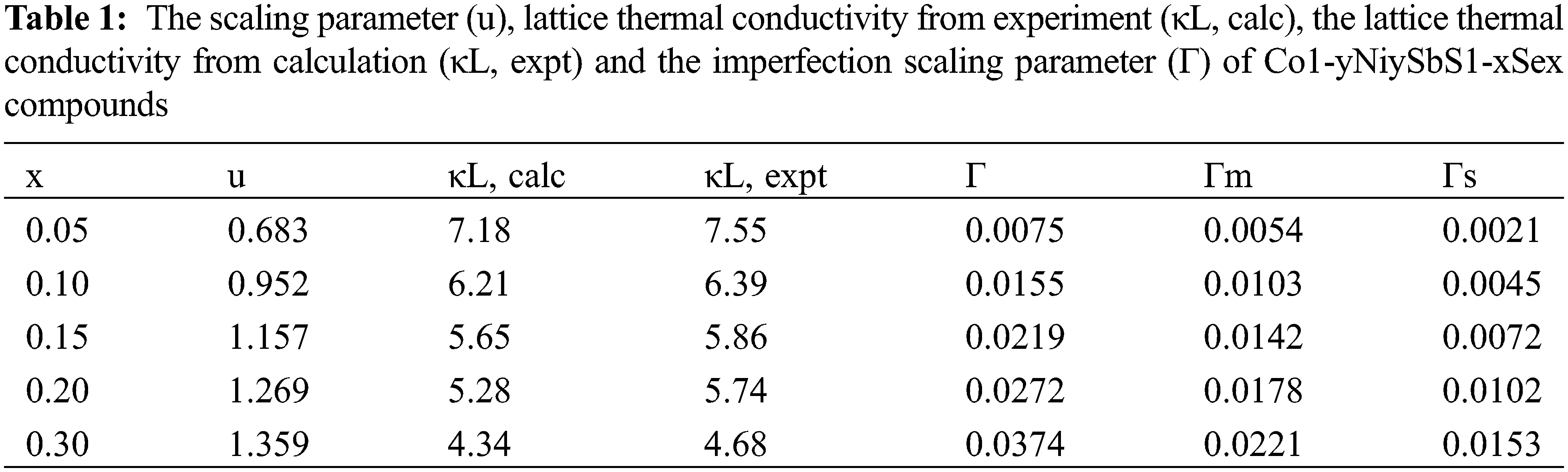
The electronic thermal conductivity of Co1−yNiySbS1−xSex (y = 0.05, 0.08, 0.1, x = 0, 0.10, 0.15) increases with increasing temperature. The lattice thermal conductivity of the material is obtained by subtracting the electronic thermal conductivity from the total thermal conductivity. Because nickel doping introduces point defects, point defects add stronger scattered phonons. When the doping amount is x = 0.1, the lattice thermal conductivity of the sample is the lowest, and the lattice thermal conductivity of the nickel-doped sample is much lower than that of the pure sample. The scattering intensity of point defects increases with the increase of nickel doping. The difference in atomic mass between cobalt and nickel atoms is small, while the difference in ionic radius and electronegativity between cobalt and nickel atoms is relatively large. The fluctuation of the stress field is greater than the influence of the fluctuation of the mass field on the thermal conductivity of the lattice. Modeling and quantitative analysis show that point defect scattering plays an important role in reducing the lattice thermal conductivity of CoSbS compounds. The ZT of Co1−yNiySbS1−xSex increases with the increase of temperature. Due to the higher power factor and lower thermal conductivity, the ZT of the solid solution selenium sample becomes significantly higher throughout the temperature range. When the solid solution of selenium (x) is less than 0.15, the ZT value of CoSbS0.85Se0.15 increases with the increase of the solid solution. When the nickel doping amount x = 0.08, the thermal conductivity increases slightly. When the nickel doping amount x = 0.1, the thermal conductivity further increases. This is mainly due to the higher thermal conductivity of the second phase, which has a certain influence on the heat transport of the sample. Obviously, in the measured temperature range, the ZT value of all samples increases with the increase of temperature. Under the condition of keeping the power factor constant, the ZT value of the single-phase doped sample increases with the increase of the nickel content due to the significant decrease of the lattice thermal conductivity. In this study, when y = 0.05−0.1, the ZT value is 300–900 K. Compared with the mother sample, the thermoelectric quality factor is improved by 135%. It can be seen from the experimental results that although Ni doping does not contribute much to improving the electrical properties of the system. However, due to the enhancement of phonon scattering by point defects, the thermal conductivity of the system is greatly reduced, and the thermoelectric performance of CoSbS is greatly improved. When the x value changes, the relevant parameters of Co1-yNiySbS1-xSex compounds are also change, as shown in Table 1.
When selenium is solid-dissolved in the position of sulfur, the XRD diffraction pattern of the uniformly expanded crystal structure constant and the volume of the unit cell is shown in Fig. 4.
Figure 4: The intensity for the Co1−yNiySbS1-xSex (y = 0.05, 0.08, 0.1, x = 0, 0.10, 0.15) compounds
Generally speaking, in the temperature range of 300–900 K, the lattice thermal conductivity decreases with the increase of temperature. When the temperature is higher than 650 K, the lattice thermal conductivity increases slowly because of the dual polarization effect. At the same time, the lattice thermal conductivity decreases with the increase of solid solution Se. The increase in the carrier concentration leads to the increase in the power factor, and at the same time, the introduction of point defects through alloying and solid solution to reduce the lattice thermal conductivity, and finally make the material Co0.9Ni0.1SbS0.85Se0.15 thermoelectric figure of merit ZT in at 923 K it is equal to 0.42. Compared with the parent material CoSbS, the thermoelectric figure of merit ZT has been greatly improved. CoSbS was prepared at a high pressure of 2P. As the temperature increases and the parameter x, y increases (x ≤ 0.1, y ≤ 0.15), The total thermal conductivity decreased from 8.3 to 3.2, the range of variation of the ZT is from 0.01 to 0.46. The relationship between thermal properties and temperature under different doping conditions is shown in Figs. 5a, 5b, which shows the thermal conductivity and hot spot value of Co1−yNiySbS1−xSex (y = 0.05, 0.08, 0.1, x = 0, 0.10, 0.15).
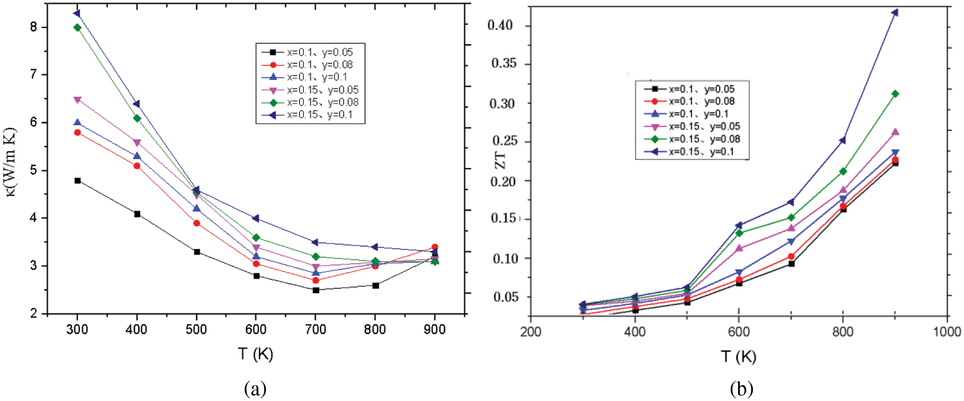
Figure 5: (a) The total thermal conductivity. (b) The ZT
6 Experiment and Conclusion Analysis
The Co1−yNiySbS1−xSex-based solid solution alloy was quickly prepared by the high-pressure sintering method. The thermoelectric properties of samples with different doping ratios y = 0.05, 0.08, 0.1, x = 0, 0.10, 0.15 were tested through experiments, and the corresponding strength was changed through the cubic structure. CoSbS is n-type. As the amount of Se doping increases, the carrier concentration of the sample increases, and its electrical transport performance is optimized. The traditional solid-phase synthesis is used to dissolve S in Se, which increases the mass fluctuation and stress fluctuation in the CoSbS system, improves the scattering probability of phonons, and effectively reduces the lattice thermal conductivity of the material. Adding a small amount of selenium can optimize three thermoelectric parameters at the same time: increase Seebeck coefficient, reduce resistivity and thermal conductivity, and improve quality factor. At the same time, the thermal and electrical properties of the bulk material were optimized by using nanoscale Ni-doped cosbs samples. Ni-doped Co sites can effectively increase the carrier concentration and effective state mass density, and improve the power factor. In addition, when x = 0.15 and y = 0.1, the ZT of Co0.9Ni0.1SbS0.85Se0.15 at the same temperature and high pressure is much higher than that of CoSbS prepared by traditional methods, which optimizes the thermoelectric performance of cosbs.
1) The Co1−yNiySbS1−xSex (0 ≤ y ≤ 0.2, 0 ≤ x ≤ 0.2)-based thermoelectric material was quickly prepared by the cubic structure high-pressure sintering method.
2) Co1−yNiySbS1−xSex is n-type conduction. With the increase of Se doping, the carrier concentration of the sample increases, and the electrical transport performance is optimized. The power factor of CoSbS0.85Se0.15 sample reaches the maximum value is 2.3 μW⋅m−1⋅K2 at 893 K.
3) The lattice thermal conductivity of CoSbS can be reduced by substituting Se for S, and the thermal and electrical properties of bulk materials can be optimized by using nanoscale Ni-doped cosbs samples. Ni doped co sites can effectively improve the carrier concentration and effective mass of density of States, and improve the power factor. The lowest lattice thermal conductivity of CoSbS0.85Se0.15 is only 2.4 W ⋅m−1⋅K−1 at 893 K, which is about 60% of that of the parent CoSbS alloy.
4) The maximum ZT value of CO0.9Ni0.1 sbS0.85Se0.15 sample was 0.46, which was about 5 times that of the parent CoSbS. Moreover, the ZT values of the samples synthesized under high pressure are higher than those of the CoSbS1−xSex samples prepared by the traditional solid phase reaction combined with SPS in the test temperature range.
Acknowledgement: The project was completed through team efforts. I would like to thank my mentors for their guidance, every member of the team, and Wuhan Technology and Business University for their support.
Funding Statement: This study greatly thanks to the support of Wuhan Technology and Business University, thanks to the research project from Natural Science Foundation of Hubei Province 2019. The item number is 2019CFC922.
Conflicts of Interest: The authors declare that they have no conflicts of interest to report regarding the present study.
1. Fu, C. G., Zhu, Y., Liu, Y. T., Xie, H. H. (2015). Band engineering of high performance p-type FeNbSb based half-Heusler thermoelectric materials for figure of merit zT > 1. Energy & Environmental Science, 8(1), 216–220. DOI 10.1039/c4ee03042g. [Google Scholar] [CrossRef]
2. Gupta, R., Bera, C. (2020). Spin-orbit coupling effect on the thermopower and power factor of CoSb. Physical Review B, 101(15), 155206. DOI 10.1103/physrevb.101.155206. [Google Scholar] [CrossRef]
3. Lou, R., Lei, M., Ding, W., Yang, W. (2021). Electronic structure and signature of Tomonaga-Luttinger liquid state in epitaxial CoSb1−x nanoribbons. npj Quantum Materials, 6(1), 89–102. DOI 10.1038/s41535-021-00381-y. [Google Scholar] [CrossRef]
4. Kuzmenkov, D., Struchalin, P., Litvintsova, Y., Delov, M., Skrytnyy, V. et al. (2022). Influence of particle size distribution on the optical properties of fine-dispersed suspensions. Fluid Dynamics & Materials Processing, 18(1), 1–14. DOI 10.32604/fdmp.2022.018526. [Google Scholar] [CrossRef]
5. Fortune, N.A., Huang, Q., Hong, T., Ma, J., Choi, E. S. et al. (2021). Evolution of magnetic-field-induced ordering in the layered structure quantum Heisenberg triangular-lattice antiferromagnet Ba3CoSb2O9. Physical Review, 103(1), 184425. DOI 10.1103/physrevb.103.184425. [Google Scholar] [CrossRef]
6. Du, Q., Abeykoon, M., Liu, Y., Kotliar, G., Petrovic, C. (2019). Low-temperature thermopower in CoSbS. Physical Review Letters, 123(7), 189–198. DOI 10.1103/physrevlett.123.076602. [Google Scholar] [CrossRef]
7. Yuan, T., Zou, M., Jin, W., Wei, X., Xu, W., et al. (2021). Pairing symmetry in monolayer of orthorhombic CoSb. Physical Review, 16(4), 43500. DOI 10.1007/s11467-020-1040-y. [Google Scholar] [CrossRef]
8. Guo, H., Liang, Y., Zhang, Z., Chen, Y. (2022). A study on the relationship between anodic oxidation and the thermal load on the aluminum alloy piston of a gasoline engine. Fluid Dynamics & Materials Processing, 18(1), 57–70. DOI 10.32604/fdmp.2022.017989. [Google Scholar] [CrossRef]
9. Tian, Y., Sirusi, A. A., Ballikaya, S., Ghassemi, N., Joseph, H. (2019). Charge-carrier behavior in Ba, Sr- and Yb-filled CoSb3: NMR and transport studies. Physical Review B, (99), 125109. DOI 10.1103/PhysRevB.99.125109. [Google Scholar]
10. Eric, B. I., Chris, W. (2019). Electronic structure and phase stability of Yb-filled CoSb3 skutterudite thermoelectrics from first principles. Chemistry of Materials, 31(6154), 11–23. DOI 10.1021/acs.chemmater.9b01630.s001. [Google Scholar] [CrossRef]
11. Yang, J. Z., Yang, D. F., Wang, Y. Q., Quan, X. J. (2021). First principles investigation of elastic and thermodynamic properties of CoSbS thermoelectric material. Journal of Solid State Chemistry, 10(302122443. DOI 10.1016/j.jssc.2021.122443. [Google Scholar] [CrossRef]
12. Parker, D., May, A. F., Wang, H., McGuire, M. A., Sales, B. C., et al. (2013). Electronic and thermoelectric properties of CoSbS and FeSbS. Physical Review B, 8(4), 271–280. DOI 10.1103/PhysRevB.87.045205. [Google Scholar] [CrossRef]
13. Chmielowski, R., Bhattacharya, S., Xie, W., Pere, D., Jacob, S. (2016). High thermoelectric performance of tellurium doped paracostibite. Chemistry of Materials, 4(15), 3094–3100. DOI 10.1039/c6tc00410e. [Google Scholar] [CrossRef]
14. Yao, W., Yang, D. F., Yan, Y. C., Peng, K. L., Zhan, H. (2017). Synergistic strategy to enhance the thermoelectric properties of CoSbS 1−x Sex compounds via solid solution. ACS Applied Materials & Interfaces, 9(12), 10595–10601. DOI 10.1021/acsami.6b12796. [Google Scholar] [CrossRef]
15. Peng, K. L., Lu, X., Zhan, H., Hui, S., Tang, X. D., (2016). Broad temperature plateau for high ZTs in heavily doped p-type SnSe single crystals. Energy & Environmental Science, 9(454), 154–161. DOI 10.1039/C5EE03366G. [Google Scholar] [CrossRef]
16. Milivojević, M. (2020). Determining Rashba spin-orbit coupling strength in InSb nanowire quantum dots: Influence of temperature and nuclear environment. Physica E: Low-Dimensional Systems and Nanostructures, 6(128), 114474(Prepublish). DOI 10.1016/j.physe.2020.114474. [Google Scholar] [CrossRef]
17. Yao, W., Yang, D. F., Yan, Y. C., Peng, K. L., Zhan, H. et al. (2017). Synergistic strategy to enhance the thermoelectric properties of CoSbS1−x Sex compounds via solid solution. ACS Applied Materials & Interfaces, 9(12), 10595–10601. DOI 10.1021/acsami.6b12796. [Google Scholar] [CrossRef]
18. Wang, H. J., Su, X. P., Sun, S. P, Wang, J. H., Jiang, Y. (2021). First-principles calculations to investigate the anisotropic elasticity and thermodynamic properties of FeAl3 under pressure effect. Results in Physics, 8(26), 26–37. DOI 10.1016/j.rinp.2021.104361. [Google Scholar] [CrossRef]
19. Njoku, I. J., Onyenegecha, C. P., Okereke, C. J., Opara, A. I., Nwaneho, F. U. (2021). Approximate solutions of Schrodinger equation and thermodynamic properties with Hua potential. Results in Physics, 24(2129), 104208. [Google Scholar]
20. Kaur, P., Bera, C. (2017). Effect of alloying on thermal conductivity and thermoelectric properties of CoAsS and CoSbS. Physical Chemistry Chemical Physics, 19(36), 24928–24933. DOI 10.1039/C7CP05170K. [Google Scholar] [CrossRef]
21. Yang, J. Z, Yang, D. F., Wang, Y. Q., Quan, X. J., Li, Y. Y. (2021). First principles investigation of elastic and thermodynamic properties of CoSbS thermoelectric material. Journal of Solid State Chemistry, 10(302), 122443. DOI 10.1016/j.jssc. [Google Scholar] [CrossRef]
 | This work is licensed under a Creative Commons Attribution 4.0 International License, which permits unrestricted use, distribution, and reproduction in any medium, provided the original work is properly cited. |