
 Submit a Paper
 Propose a Special lssue
 Open Access
ARTICLE

Modular System of Cascaded Converters Based on Model Predictive Control
School of Electrical and Control Engineering, North China University of Technology, Beijing, 100144, China
* Corresponding Author: Yaoquan Wei. Email:
Energy Engineering 2024, 121(11), 3241-3261. https://doi.org/10.32604/ee.2024.051810
Received 15 March 2024; Accepted 15 May 2024; Issue published 21 October 2024
 View Full Text
 Download PDF
Abstract
A modular system of cascaded converters based on model predictive control (MPC) is proposed to meet the application requirements of multiple voltage levels and electrical isolation in renewable energy generation systems. The system consists of a Buck/Boost + CLLLC cascaded converter as a submodule, which is combined in series and parallel on the input and output sides to achieve direct-current (DC) voltage transformation, bidirectional energy flow, and electrical isolation. The CLLLC converter operates in DC transformer mode in the submodule, while the Buck/Boost converter participates in voltage regulation. This article establishes a suitable mathematical model for the proposed system topology, and uses MPC to control the system based on this mathematical model. Module parameters are designed and calculated, and simulation is built in MATLAB/Simulink to complete the simulation comparison experiment between MPC and traditional proportional integral (PI) control. Finally, a physical experimental platform is built to complete the physical comparison experiment. The simulation and physical experimental results prove that the control accuracy and response speed of MPC are better than traditional PI control strategy.Keywords
Nomenclature
| MPC | Model predictive control |
| IPOS | Input parallel output series system |
| ISOP | Input series output parallel |
| FHA | First harmonic approximation |
| DC | Direct-current |
| DAB | Dual active full bridge converter |
| ZVS | Zero voltage switch |
| DCX | DC transformer characteristics |
| ZCS | Zero current switching |
The increasingly serious global energy crisis has brought new challenges to the power industry of countries around the world. With the development and application of new energy, distributed photovoltaic and wind power generation have received increasing attention and research in recent years [1–3]. To achieve the matching of photovoltaic array and wind turbine output with the voltage level of the DC distribution network, high-power isolated bidirectional DC-DC converters are usually used [4–7].
Due to the pursuit of power density in converters, high-frequency converters often face issues such as switching losses. Therefore, high-frequency switches must achieve soft switching, and DC-DC converters with soft switching characteristics are gradually receiving attention [8–10]. The dual active full bridge (DAB) converter is currently the most widely used converter due to its simple structure and advantages such as soft switching. Reference [11] proposes a voltage matching (VM) control for a hybrid bridge-based DAB converter, which is used for a wide range of voltage conversion gain applications. The proposed VM control can achieve a wide transformation gain, decoupling of two power control variables, and a wide range of zero voltage switching (ZVS). Reference [12] proposes an Input Series Output Parallel (ISOP) DAB DC-DC converter and applies an input-oriented power sharing control method with fast dynamic response to ensure the power sharing capability and fast dynamic performance of the converter. However, there are still some problems with the DAB converter, such as the variation of ZVS range with load changes, the presence of circulating currents inside the converter, and high inductance current stress. In order to solve the problem of ZVS variation of DAB converter with load changes, some scholars have proposed LLC resonant converter. Reference [13] studies the application of LLC resonant converters in input parallel and output parallel systems, and proposed a model for the I-V characteristics of the output port and small signal output impedance of charge-controlled LLC converters. Reference [14] proposes a DAB-LLC-DCX DC-DC converter for load point applications, which features an integrated magnet and a shared rectifier, enabling strict voltage regulation, ZVS operation of all switches, and zero current switching operation of the rectifier. However, due to the asymmetric resonance parameters of the primary and secondary sides of the LLC converter, the bi-directional gain is not uniform, resulting in inconsistent bi-directional operating characteristics of the converter, and the converter may not be able to operate at the optimal operating point. To solve the problem of forward and reverse differences in LLC converters, some scholars have improved the topology of LLC resonant circuits and proposed the CLLLC resonant converter. Reference [15] proposes a hybrid modulation method based on a CLLLC converter, which uses frequency modulation (FM) with an undervoltage gain greater than 1 and phase shift modulation (PSM) with an undervoltage gain less than 1. Simultaneously, the extended descriptive function modeling method was used to establish both large signal and small signal models. Reference [16] proposes a novel soft start control strategy by discussing the factors that affect current and voltage stress during the start-up time and process of CLLLC converters.
In addition, in renewable energy generation systems, switch tubes need to withstand high voltage stress, so higher-rated voltage requirements are required for switch tubes, which increases hardware costs. To solve this problem, many scholars have proposed many methods to reduce the voltage stress of switch tubes [17–19]. High voltage switch series connection technology is to connect a group of switching tubes in series to the high voltage side, equivalent to a switch, so as to reduce the voltage stress of the switching tubes. Reference [20] proposes a novel active gate driver approach with a variable gate voltage regulator (GVR), which uses a single P-channel MOSFET to determine the connection timing of a precharged capacitor connected in series with the input capacitor, allowing for adjustment of the switching transient of each device in the stack. Reference [21] proposes an active voltage balancing method suitable for two series connected devices, which applies a multi winding coupled inductor with low turns to achieve voltage deviation sampling and high-quality signal isolation. The multi-level converter proposed in the 1980s reduced the voltage stress of the switching tube, made it easy to expand, and had high power density. At the same time, due to the three levels of midpoint voltage in each bridge arm, its output voltage harmonics were small. Reference [22] proposes a novel modular multilevel DC-DC converter with high power density potential. The proposed hybrid converter combines the modular advantages of modular multilevel converters (MMC) and the efficient frequency advantages of flying capacitor converters. Reference [23] proposes an exhaustive active set method to implement a modulation MPC scheme, enabling MMC to operate over a wide frequency range. Multiple converters in series and parallel are often used in high-voltage and high-power situations. By combining modules, the voltage and current stress of each module is reduced, while also reducing the stress of each module component. It is also easy to achieve system expansion and maintenance, and the combination of multiple modules also improves system redundancy. Reference [24] proposes an ISOP isolated bidirectional DC converter and based on this topology, proposed a three-loops input voltage sharing (IVS) control strategy. Reference [25] proposes an asymmetric pulse width modulation (PWM) scheme to address the output voltage imbalance and voltage gain issues of input parallel output series (IPOS) converters at D < 0.5. With this scheme, when D < 0.5, the natural output voltage balance and high boost to boost conversion ratio can be extended.
The key to the safe and reliable operation of cascaded converter systems lies in having a good operational control strategy. Many studies have been conducted on the control strategy of cascaded converters [26–28]. Reference [29] proposes a coordinated control scheme for cascaded converters, which only uses a proportional DC link voltage regulator, reducing system types while maintaining accurate DC link voltage tracking. Reference [30] proposes a new control method based on Lyapunov function to eliminate stability issues caused by changes in device parameters in cascaded converters. Reference [31] introduces a MPC for cascaded converters used in solid-state transformers. The proposed method reduces the number of states to be considered in the control, thereby shortening the calculation time and simplifying the expansion of the flying capacitor bridge. The modular system of cascaded converters is a nonlinear system with multiple inputs and multiple outputs, and the variables are coupled with each other. MPC can achieve multi-objective control without linearization, which is a nonlinear optimization control method with the advantages of simple control and strong robustness. It has great advantages in dealing with complex constrained optimization problems in nonlinear systems [32,33].
Based on the above, this article proposes a modular system of cascaded converters applied to renewable energy generation systems. The comparison between the proposed system topology and the existing topology is shown in Table 1. The system consists of a Buck/Boost + CLLLC cascaded converter as a submodule, which is combined in series and parallel on the input and output sides to form a DC transformer system, achieving DC voltage transformation, bidirectional energy flow, and electrical isolation in the data center. In the submodule, the CLLLC converter operates in DC transformer mode, while the Buck/Boost converter participates in voltage regulation. In addition, a MPC strategy based on submodules is proposed to achieve the problem of voltage and current sharing between modules. Compared with traditional PI control strategies, it improves the accuracy and efficiency of system control.
This article is organized as follows. Section 2 introduces the proposed modular system of cascaded converters and its working principle. Based on the working principle, Section 3 establishes a mathematical model of the system submodules. Section 4 designs and calculates the parameters of the system converter. Section 5 conducts simulation experiments and compares them with PI control simulation experiments to verify the superiority of the proposed control strategy. Section 6 conducts physical experiments and compares them with PI controlled physical experiments to verify the effectiveness of the proposed control strategy. Finally, Section 7 concludes.
2 System Topology and Working Principle
2.1 System Topology and Submodule Topology
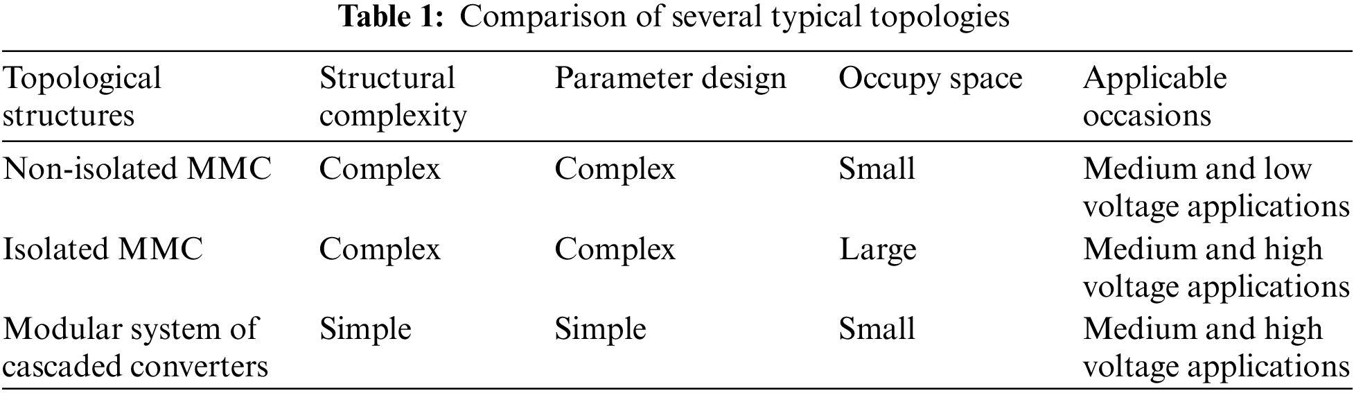
The topology structure of the modular system of cascaded converters is shown in Fig. 1, which is composed of several Buck/Boost + CLLLC cascaded converter submodules combined in series and parallel. Among them, the high-voltage side modules are connected in series, and the low-voltage side modules are connected in parallel.
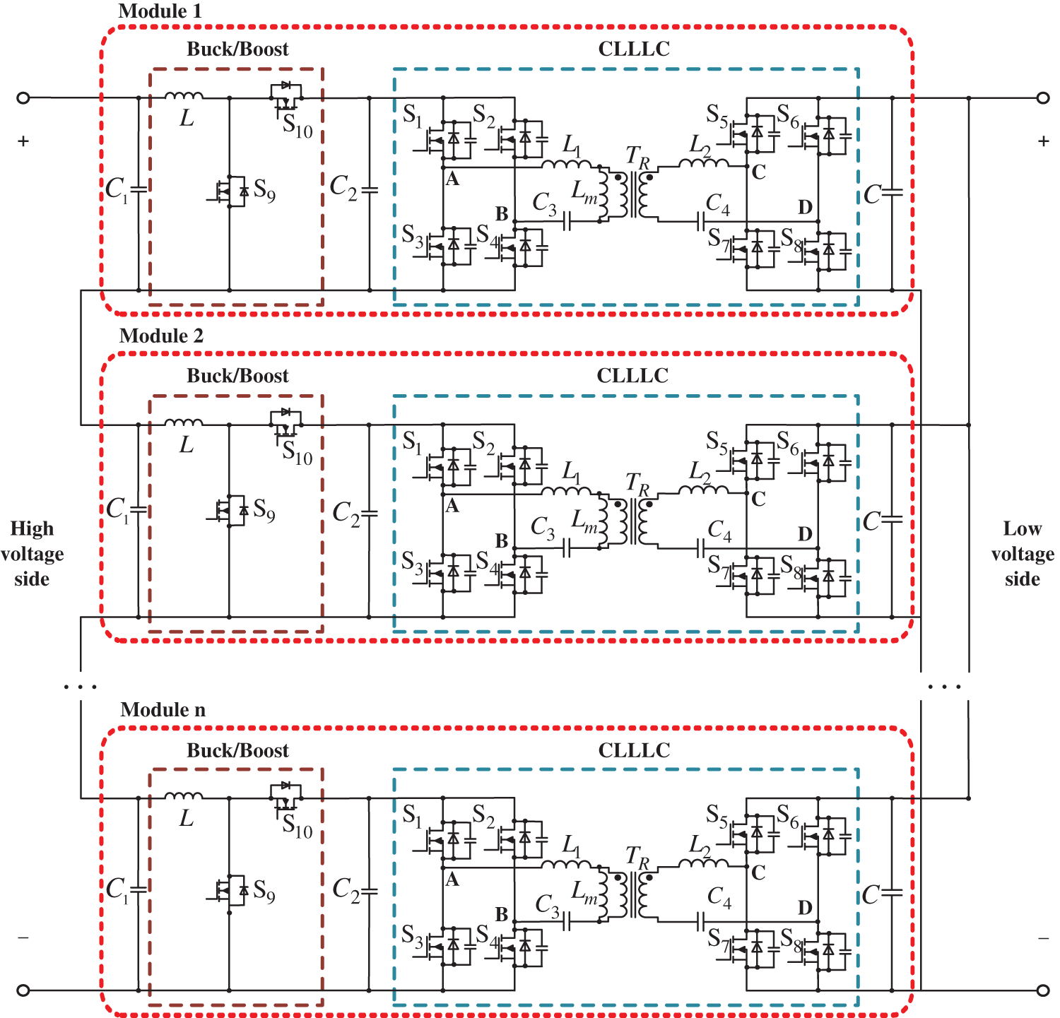
Figure 1: System structure topology diagram
The topology diagram of the system submodule is shown in Fig. 2. The front stage is the CLLLC converter. In order to achieve higher efficiency of the CLLLC converter, it can operate near the resonant frequency and achieve the DC transformer characteristics (DCX) through reasonable parameter design; The back stage is a Buck/Boost converter that operates in voltage regulation mode and matches the input and output voltage.
Figure 2: Submodule topology diagram
The power flow of a cascaded converter from the low voltage side to the high voltage side is defined as forward operation, and vice versa is defined as reverse operation. During forward operation, S1~S4 apply a control drive signal, S5~S8 apply a synchronous rectification control drive signal, S9 applies a control drive signal, S10 always turns off, and its bypass diode works. At this time, the subsequent converter is equivalent to a Boost converter. When running in reverse, S5~S8 apply a control drive signal, S1~S4 apply a synchronous rectification control drive signal, S10 applies a control signal, S9 always turns off, and its bypass diode works.
The main working waveform of the cascaded converter is shown in Fig. 3, with 8 modes stored in one working cycle. Fig. 3a shows the working waveform of the CLLLC converter, and Fig. 3b shows the working waveform of the Buck/Boost converter. The energy flow paths under each mode are shown in Figs. 4 to 7, and the operation process of each mode is analyzed in combination with Fig. 3.
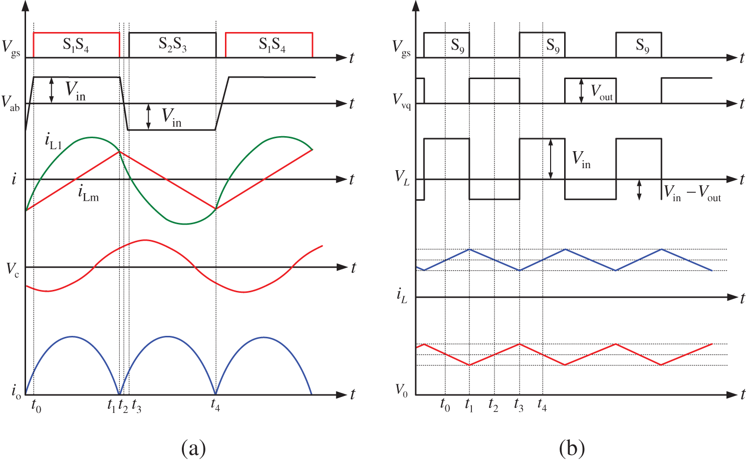
Figure 3: Working waveform diagram of cascaded converter. (a) Working waveform of CLLLC converter. (b) Working waveform of Buck/Boost converter
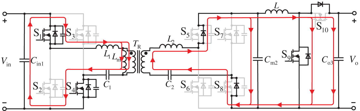
Figure 4: Working mode 1
Working mode 1 (t0~t1): As shown in Fig. 4, initially, S1 and S4 achieve ZVS and S9 is turned on. Due to the sufficiently large excitation inductance Lm, it has a strong blocking effect on the excitation current, and the excitation current iLm and resonance current iLr increase at different speeds. The difference between excitation current and resonant current flows towards the secondary side, and at this time, the secondary side switch is conducting. In addition, the current of inductor L increases linearly at a certain ratio, and inductor L stores energy. At time t1, the resonant current iLr is equal to the excitation current iLm, and mode 1 ends.
Working mode 2 (t1~t2): As shown in Fig. 5, at time t1, iLm = iLr, energy only flows in the primary side, and the current in the secondary diode circuit gradually becomes zero and automatically turns off, achieving zero current switching (ZCS). At this time, S9 turns off. Due to the current holding characteristics of the inductor, the current flowing through inductor L does not immediately become zero, but slowly decreases. In addition, the voltage at both ends of the load is provided by capacitors.
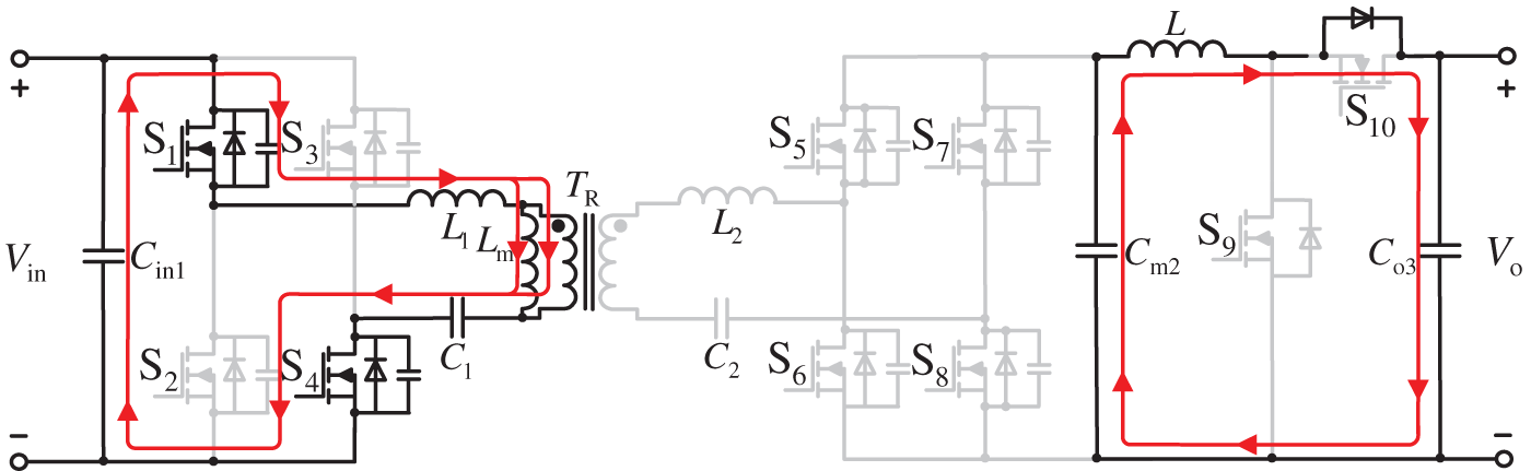
Figure 5: Working mode 2
Working mode 3 (t2~t3): As shown in Fig. 6, S1~S4 turn off from time t2, and S9 continues to maintain the off state. The resonant current starts to charge the parasitic capacitors of S1 and S4 to the input voltage Vin, while the parasitic capacitors of S2 and S3 discharge to zero voltage. The current flowing through inductor L continues to decrease until it reaches zero. When the charging and discharging are completed, this mode ends. In this mode, the rectifier network has no voltage output, and the output voltage is maintained by the capacitor.

Figure 6: Working mode 3
Working mode 4 (t3~t4): As shown in Fig. 7, parasitic capacitors of S2 and S3 have been discharged at the end of the previous mode, preparing for ZVS of S2 and S3. The resonant current flows through the parasitic diodes of S2 and S3, and the energy flows from the primary side to the secondary side. At t4, the ZVS switch of S2 and S3 is turned on, and the resonant current flows through the switch. S9 is reopened, and the inductor L stores energy. This mode ends.
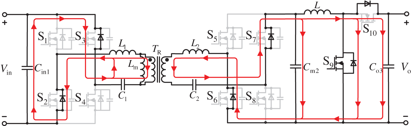
Figure 7: Working mode 4
The last four operating modes are in opposite directions to the first four operating modes. Similarly, it can be concluded that the operating mode of the cascaded sub converter is the same as the forward operating mode when operating in reverse, with the only difference being that the rear converter becomes the front converter during forward operation, which functions similarly to a Buck converter.
The modular system of cascaded converters proposed in this article is a nonlinear system with multiple inputs and outputs, and the variables are coupled with each other. For its submodules, if traditional PI dual loop control is used, the entire control system uses a total of 4 PI controllers, and the inner loop PI parameters are not the same when power flows in both directions. Therefore, at least 8 PI controller parameters need to be adjusted during normal operation of the system submodules, especially during wide range operation, which is very difficult to achieve and it is difficult to ensure optimal system performance. Given the drawbacks of traditional dual loop control methods, this paper introduces the MPC concept and proposes a MPC method for Buck/Boost + CLLLC cascaded converters. The control block diagram is shown in Fig. 8.

Figure 8: System control block diagram
From Fig. 8, it can be seen that MPC optimizes parameters based on the dynamic mathematical model of the system, and outputs control variables in real time according to the feedback voltage and current values for control. In addition, MPC has three major features: predictive model, rolling optimization, and feedback correction. It is particularly important to establish a suitable and correct mathematical model. This article will conduct a detailed mathematical model establishment in the next section.
This article first establishes independent mathematical models for the Buck/Boost converter and the CLLLC converter, and obtains equivalent circuit models, as shown in Figs. 9 and 10, where n = 1-D, D is the duty cycle of the Buck/Boost converter. Then, by cascading the circuit models at all levels, the equivalent circuit model of the cascaded converter is obtained, as shown in Fig. 11, where V1 = Vm, V2 = K2Vo, C1 = Cs1, C2 = Cs2, R1 = Rs1, R2 = K2Rs2 and K are the TR ratio of the transformer. Based on this circuit model, a mathematical model of the cascaded converter system is established.

Figure 9: Equivalent circuit diagram of Buck/Boost converter
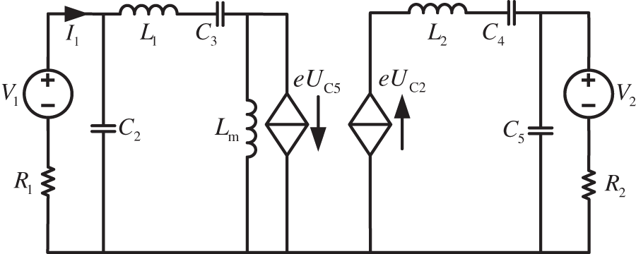
Figure 10: Equivalent circuit diagram of CLLLC converter
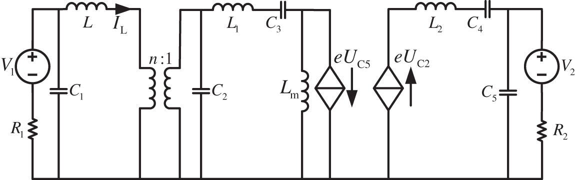
Figure 11: Equivalent circuit diagram of Buck/Boost + CLLLC cascaded converter
In the cascaded converter, the DC voltage gain MBB of the Buck/Boost converter and the DC voltage gain MCLLLC of the CLLLC converter have no mutual influence. Therefore, according to the equivalent circuit diagram shown in Fig. 11, the DC voltage gain M of the cascaded converter is:
Similarly, according to the equivalent circuit diagram shown in Fig. 11, the input-output transfer function G of the Buck/Boost + CLLLC cascaded converter is equal to the product of the input-output transfer function Gxu of the Buck/Boost converter and the input-output transfer function H(jωs) of the CLLLC converter:
Average each mode within one switching cycle to obtain the Buck/Boost converter state space average model:
Among them,
When the static point
Taking input variable
Introducing low-frequency small signal perturbations
Among them,
The transfer function between state variables
Among them,
According to Fig. 10, the input-output transfer function of the CLLLC resonant converter is obtained as follows:
Among them,
By defining
When the converter operates at the resonant operating point, the imaginary part of the transfer function is zero. At this time, the expression of the resonant frequency x containing the resonant network can be obtained from Eq. (9) as follows:
Solved,
Among them,
By defining the normalized frequency
Furthermore, the voltage gain of the CLLLC resonant converter can be obtained as:
When the switching tube operates at the resonant point, by substituting Eq. (12) into Eq. (14), the gain of the converter in quasi resonant operating state is:
Substitute Eqs. (5) and (15) into Eq. (1) to obtain the DC voltage gain M of the Buck/Boost + CLLLC cascaded converter as follows:
Substitute Eqs. (7) and (13) into Eq. (2) to obtain the input-output transfer function G of the Buck/Boost + CLLLC cascaded converter as follows:
The design specifications of the Buck/Boost + CLLLC cascaded converter proposed in this article are: high voltage V1 of 134 V, low voltage V4 of 48 V, intermediate stage voltage Vm of 72 V, and rated power P of 500 W. Calculate and design parameters according to design requirements.
The relationship between the resonant network gain M of the CLLLC converter and the transformer ratio n is:
Due to the DC transformer characteristics of the CLLLC resonant converter, the resonant network gain of the converter is approximately equal to 1. According to Eq. (18), the transformer ratio is calculated to be 1.5.
In the working mode, it was mentioned that the excitation current in the freewheeling mode will charge and discharge the switch junction capacitor, preparing for the next ZVS. Therefore, the maximum value of excitation inductance can be obtained as:
where
According to the switch tube model used in the experiment, the maximum excitation inductance can be calculated to be 187 μH. To reduce the volume of the transformer and the impact of stray parameters on the resonant network, the integrated leakage inductance of the transformer is used as the resonant inductance in the resonant network. The size of the leakage inductance affects the design of the transformer. Therefore, the k value is selected as 20 and the excitation inductance Lm is 40 μH. The resonant inductance L1 is 2 μH.
Due to the design of the converter working at the optimal operating point, i.e., the resonant point, the resonant capacitance can be calculated based on the calculated resonant inductance
The parameters of the transformer primary and secondary resonance network are equivalent, and the secondary resonance parameters can be obtained as:
According to Eqs. (23) and (24), the inductance value of the Buck/Boost converter operating in Buck and Boost modes can be obtained as follows:
According to the input and output voltage, the duty cycle can be obtained as:
From Eqs. (23)–(25),
Assuming that there is no freewheeling process in the Buck/Boost converter and all current flows to the load, it can be concluded that the input capacitance of the converter should meet the following requirements:
Among them, R represents the equivalent output load of the submodule to the Buck/Boost output load. To meet the requirement of less than 5% voltage fluctuation on the output side, the input capacitance of the converter can be obtained by inputting the parameter, which is 100 μF. The output capacitance is 120 μF.
In summary, the parameter design of the Buck/Boost + CLLLC cascaded converter is shown in Table 2.

Based on the mathematical model established in Section 3 and the obtained control quantity expression, use MATLAB to write an MPC control algorithm program, and build a simulation model in MATLAB/simulink for simulation experiments, and compare it with traditional PI control strategies. Build simulation model of input parallel output series (IPOS) system with three sub modules to simulate the sudden changes in input voltage and output load of the system.
5.1 Simulation Experiment of Input Voltage Changes Suddenly
Fig. 12a,b shows the voltage waveform comparison and current waveform comparison of the system under PI control and MPC control strategies when the input voltage of the system undergoes a sudden change. When the input voltage undergoes a sudden change, under the traditional PI control strategy, it takes 90 ms for the system to stabilize, and there is a significant difference in the output voltage and current values compared to before the change in operating conditions. The voltage value increases by 13 V compared to before, and the current value increases by 0.12 A compared to before. At the moment of the sudden change, the voltage drops by 13 V, and the current drops by 0.12 A; Under the MPC control strategy, after 60 ms of system stability, there was no significant difference in voltage and current values compared to before the change in operating conditions. At the moment of sudden change, the voltage dropped by 11 V and the current dropped by 0.1 A.
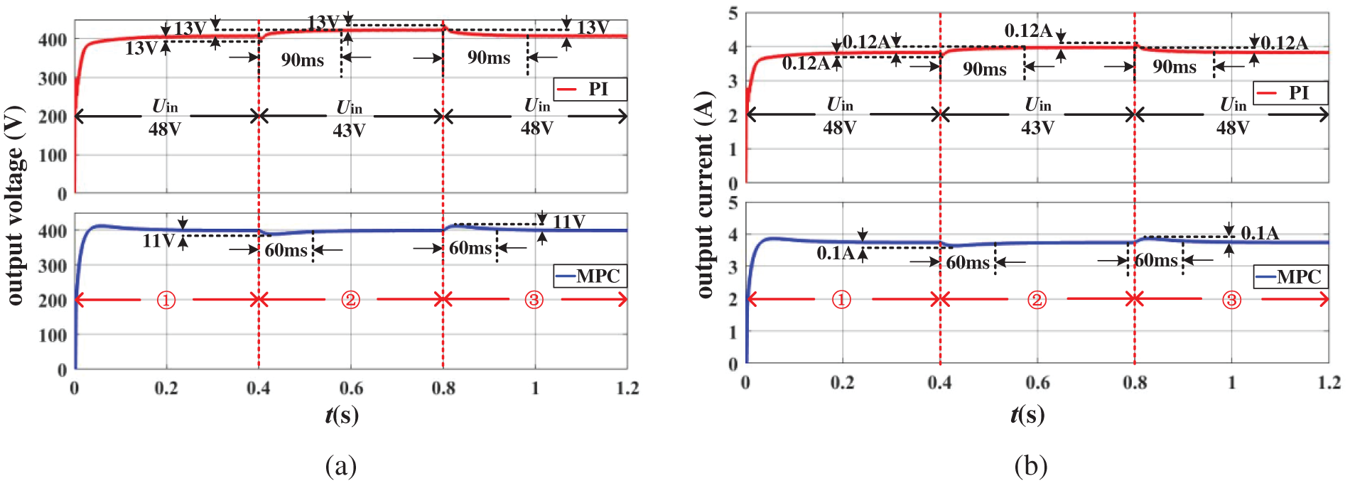
Figure 12: Waveform diagram of input voltage changes suddenly in IPOS system. (a) Voltage waveform comparison chart. (b) Current waveform comparison chart
5.2 Simulation Experiment of Output Load Changes Suddenly
Fig. 13a,b respectively shows the voltage waveform comparison and current waveform comparison of the system under PI control and MPC control strategies when the system output load undergoes a sudden change.

Figure 13: Waveform diagram of output load changes suddenly in IPOS system. (a) Voltage waveform comparison chart. (b) Current waveform comparison chart
When the output load undergoes a sudden change, under the traditional PI control strategy, the system stabilizes after 90 ms, and there is a significant difference in the output voltage and current values compared to before the change in operating conditions. The voltage value increases by 12 V, and the voltage drops by 12 V and current drops by 0.2 A at the moment of the sudden change; Under the MPC control strategy, after 60 ms of system stability, there was no significant difference in voltage and current values compared to before the change in operating conditions. At the moment of sudden change, the voltage dropped by 10 V and the current dropped by 0.14 A.
In summary, under the MPC control strategy, the dynamic performance of the modular system of cascaded converters is superior to traditional PI control, and the control accuracy and stability are significantly improved compared to PI control.
In order to further validate the proposed converter parameter design and MPC strategy, an experimental platform was built based on the designed parameters. The physical platform of a single submodule is shown in Fig. 14a. Connect the two submodules on the high-voltage and low-voltage sides in series and parallel to form an IPOS system, as shown in Fig. 14b. The input voltage of the system is 48 V, the output voltage is approximately 270 V, and the maximum output current is 1.5 A.

Figure 14: Experimental platform. (a) Sub module physical platform. (b) Physical experiment platform
6.1 Physical Experiment of Input Voltage Changes Suddenly
Fig. 15a,b shows the waveform of the output voltage of each module and the system output voltage and current when the input voltage suddenly changes between 48–43 V in the IPOS system under PI control strategy. Fig. 16a,b shows the waveform of the output voltage of each module and the system output voltage and current when the input voltage suddenly changes between 48–43 V in the IPOS system under MPC control strategy. From the graph, it can be seen that after a sudden increase or decrease in input voltage, the instantaneous output voltage under both control strategies will slightly increase or decrease. However, under the MPC strategy, the amplitude of the instantaneous output voltage increases or decreases is small, and the time required to restore steady state is short, that is, the dynamic response is fast. In addition, under this operating condition, all modules can evenly share the output voltage.

Figure 15: Waveform diagram of output voltage of each module and system output voltage and current under PI control. (a) Input voltage suddenly changes to 48 V. (b) Input voltage suddenly changes to 43 V
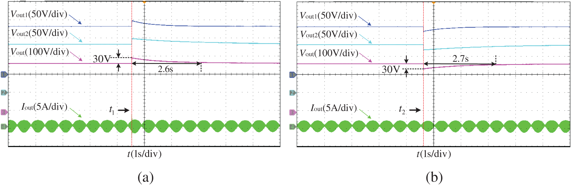
Figure 16: Waveform diagram of output voltage of each module and system output voltage and current under MPC control. (a) Input voltage suddenly changes to 48 V. (b) Input voltage suddenly changes to 43 V
6.2 Physical Experiment of Output Load Changes Suddenly
Fig. 17a,b shows the waveform of the output voltage of each module and the system output voltage and current when the output load of the IPOS system suddenly changes between 400 and 100 W under PI control strategy.
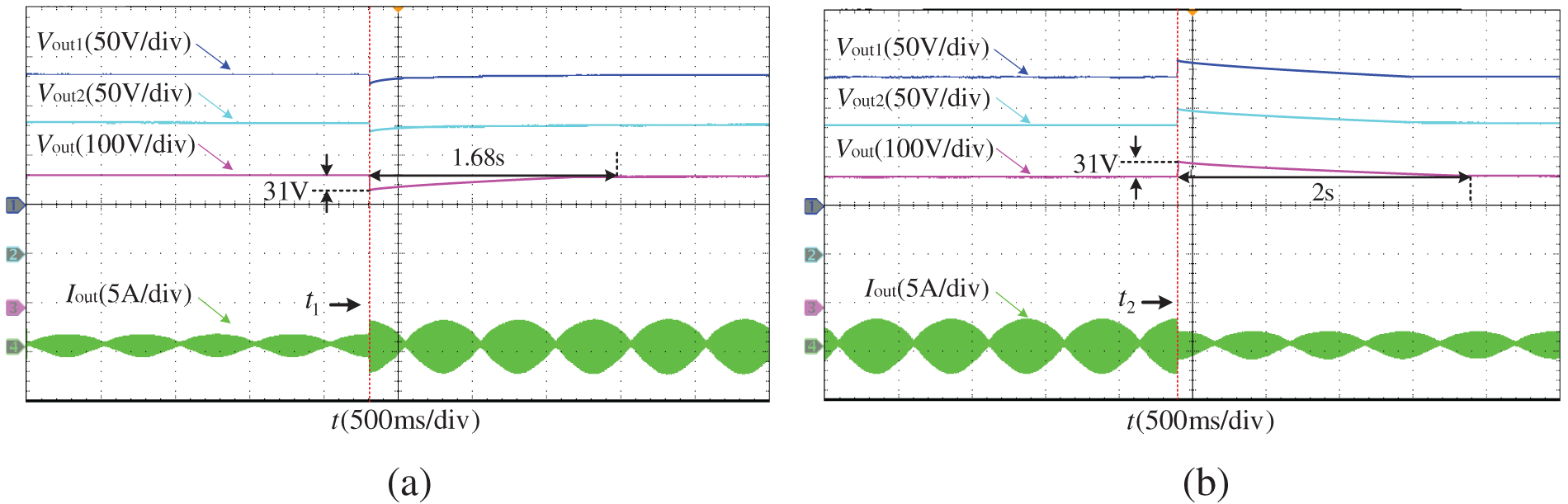
Figure 17: Waveform diagram of output voltage of each module and system output voltage and current under PI control. (a) Output load suddenly changes to 400 W. (b) Output load suddenly changes to 100 W
Fig. 18a,b shows the waveform of the output voltage of each module and the system output voltage and current when the input voltage suddenly changes between 400 and 100 W in the IPOS system under MPC control strategy. From the graph, it can be seen that after a sudden increase or decrease in output load, the output voltage of each module and the system output voltage under both control strategies will have a small overshoot, and can be stable after transient processes. However, under the MPC strategy, the instantaneous output voltage rise or fall is small, and the dynamic response is fast. In addition, under this operating condition, all modules can evenly share the output voltage.

Figure 18: Waveform diagram of output voltage of each module and system output voltage and current under MPC control. (a) Output load suddenly changes to 400 W. (b) Output load suddenly changes to 100 W
This article uses a Buck/Boost + CLLLC cascaded converter as a submodule. It forms the modular system of cascaded converters studied in this paper by connecting the high-voltage side in series and the low-voltage side in parallel. An analysis was conducted on the working principle of the proposed system, a suitable and correct mathematical model was established, module parameters were designed, and simulation models of the IPOS system and ISOP system under the PI control strategy and MPC control strategy were built. Simulation comparative experiments were completed, and finally, the differences between the two control strategies were analyzed and compared through physical comparative experiments. The main conclusion is:
(1) A modular system of cascaded converters topology applied to renewable energy generation systems was proposed, and its working principle was analyzed. Based on the working principle, the equivalent circuit of the Buck/Boost + CLLLC cascaded converter was obtained, and a correct mathematical model was established to prepare for the implementation of the MPC strategy. Suitable module parameters were designed.
(2) Build a simulation model and conduct comparative experiments between MPC control strategy and traditional PI control strategy. The results show that MPC has a faster dynamic response and better control accuracy than PI. The superiority of MPC has been preliminarily verified through simulation experiments.
(3) Build a hardware experimental platform and conduct comparative experiments on the multi-operating conditions of IPOS and ISOP systems under two control strategies to verify the feasibility and effectiveness of the proposed MPC strategy, which can achieve stable operation of the system.
Acknowledgement: None.
Funding Statement: The study was supported by the National Key Research and Development Plan, Grant/Award Number: 2018YFB1503005.
Author Contributions: The authors confirm contribution to the paper as follows: study conception and design: Chunxue Wen, Yaoquan Wei and Peng Wang; data collection: Jianlin Li, Jinghua Zhou and Qingyun Li; analysis and interpretation of results: Yaoquan Wei, Peng Wang and Qingyun Li; draft manuscript preparation: Chunxue Wen, Yaoquan Wei and Peng Wang. All authors reviewed the results and approved the final version of the manuscript.
Availability of Data and Materials: Data supporting this study are included within the article.
Ethics Approval: Not applicable.
Conflicts of Interest: The authors declare that they have no conflicts of interest to report regarding the present study.
References
1. G. F. Gontijo, T. Kerekes, D. Sera, M. Ricco, L. Mathe and R. Teodorescu, “Medium-voltage converter solution with modular multilevel structure and decentralized energy storage integration for high-power wind turbines,” IEEE Trans. Power Electron., vol. 36, no. 11, pp. 12954–12967, Nov. 2021. doi: 10.1109/TPEL.2021.3077501. [Google Scholar] [CrossRef]
2. H. Wang, M. Rasheed, R. Hassan, M. Kamel, S. Tong and R. Zane, “Life-extended active battery control for energy storage using electric vehicle retired batteries,” IEEE Trans. Power Electron., vol. 38, no. 6, pp. 6801–6805, Jun. 2023. doi: 10.1109/TPEL.2023.3252362. [Google Scholar] [CrossRef]
3. S. Wang, Y. Xie, Z. Zhang, L. Zhu, and D. Zhao, “Research on energy availability and economy coupling of distributed energy supply system in data center,” in 2020 IEEE Sustain. Power and Energy Conf. (iSPEC), Chengdu, China, 2020, pp. 1893–1898. [Google Scholar]
4. C. -S. Wang, S. -H. Zhang, Y. -F. Wang, B. Chen, J. -H. Liu, “A 5-kW isolated high voltage conversion ratio bidirectional CLTC resonant DC-DC converter with wide gain range and high efficiency,” IEEE Trans. Power Electron., vol. 34, no. 1, pp. 340–355, Jan. 2019. doi: 10.1109/TPEL.2018.2823082. [Google Scholar] [CrossRef]
5. J. Lu, Y. Wang, X. Li, and C. Du, “High-conversion-ratio isolated bidirectional DC-DC converter for distributed energy storage systems,” IEEE Trans. Power Electron., vol. 34, no. 8, pp. 7256–7277, Aug. 2019. doi: 10.1109/TPEL.2018.2881085. [Google Scholar] [CrossRef]
6. Y. -E. Wu and Y. -T. Ke, “A novel bidirectional isolated DC-DC converter with high voltage gain and wide input voltage,” IEEE Trans. Power Electron., vol. 36, no. 7, pp. 7973–7985, Jul. 2021. doi: 10.1109/TPEL.2020.3045986. [Google Scholar] [CrossRef]
7. V. Sidorov, A. Chub, and D. Vinnikov, “Bidirectional isolated hexamode DC-DC converter,” IEEE Trans. Power Electron., vol. 37, no. 10, pp. 12264–12278, Oct. 2022. doi: 10.1109/TPEL.2022.3170229. [Google Scholar] [CrossRef]
8. Y. Shi, X. -W. Gui, J. Xi, X. Wang, X. Yang, “Large power hybrid soft switching mode PWM full bridge DC-DC converter with minimized turn-on and turn-off switching loss,” IEEE Trans. Power Electron., vol. 34, no. 12, pp. 11629–11644, Dec. 2019. doi: 10.1109/TPEL.2019.2904982. [Google Scholar] [CrossRef]
9. R. Faraji, H. Farzanehfard, G. Kampitsis, M. Mattavelli, E. Matioli and M. Esteki, “Fully soft-switched high step-up nonisolated three-port DC-DC converter using GaN HEMTs,” IEEE Trans. Ind. Electron., vol. 67, no. 10, pp. 8371–8380, Oct. 2020. doi: 10.1109/TIE.2019.2944068. [Google Scholar] [CrossRef]
10. M. R. S. de Carvalho, E. A. O. Barbosa, F. Bradaschia, L. R. Limongi, and M. C. Cavalcanti, “Soft-switching high step-up DC-DC converter based on switched-capacitor and autotransformer voltage multiplier cell for PV systems,” IEEE Trans. Ind. Electron., vol. 69, no. 12, pp. 12886–12897, Dec. 2022. doi: 10.1109/TIE.2022.3142432. [Google Scholar] [CrossRef]
11. G. Xu, D. Sha, Y. Xu, and X. Liao, “Hybrid-bridge-based DAB converter with voltage match control for wide voltage conversion gain application,” IEEE Trans. Power Electron., vol. 33, no. 2, pp. 1378–1388, Feb. 2018. doi: 10.1109/TPEL.2017.2678524. [Google Scholar] [CrossRef]
12. N. Hou, P. Gunawardena, X. Wu, L. Ding, Y. Zhang and Y. W. Li, “An input-oriented power sharing control scheme with fast-dynamic response for ISOP DAB DC-DC converter,” IEEE Trans. Power Electron., vol. 37, no. 6, pp. 6501–6510, Jun. 2022. doi: 10.1109/TPEL.2021.3138126. [Google Scholar] [CrossRef]
13. S. S. Shah, S. K. Rastogi, and S. Bhattacharya, “Paralleling of LLC resonant converters,” IEEE Trans. Power Electron., vol. 36, no. 6, pp. 6276–6287, Jun. 2021. doi: 10.1109/TPEL.2020.3040621. [Google Scholar] [CrossRef]
14. M. Wang et al., “Hybrid control strategy for an integrated DAB-LLC–DCX DC-DC converter to achieve full-power-range zero-voltage switching,” IEEE Trans. Power Electron., vol. 36, no. 12, pp. 14383–14397, Dec. 2021. doi: 10.1109/TPEL.2021.3086633. [Google Scholar] [CrossRef]
15. K. Li et al., “Modeling and hybrid controller design of CLLLC,” in IEEE 10th Int. Symp. Power Elect. for Distrib. Generat. Syst. (PEDG), Xi’an, China, 2019, pp. 168–172. [Google Scholar]
16. Y. Tang, S. C. Gong, and S. J. Xie, “Research on open-loop soft-start strategy of CLLLC bi-directional resonant converter,” in 2018 IEEE Int. Power Elect. Appl. Conf. Expo. (PEAC), Shenzhen, China, 2018, pp. 1–6. [Google Scholar]
17. P. Talebi, M. Packnezhad, and H. Farzanehfard, “Fully soft-switched ultra-high step-up converter with very low switch voltage stress,” IEEE Trans. Power Electron., vol. 38, no. 3, pp. 3523–3530, Mar. 2023. doi: 10.1109/TPEL.2022.3224831. [Google Scholar] [CrossRef]
18. S. Sadaf, M. S. Bhaskar, M. Meraj, A. Iqbal, and N. Al-Emadi, “A novel modified switched inductor boost converter with reduced switch voltage stress,” IEEE Trans. Ind. Electron., vol. 68, no. 2, pp. 1275–1289, Feb. 2021. doi: 10.1109/TIE.2020.2970648. [Google Scholar] [CrossRef]
19. K. R. Kothapalli, M. R. Ramteke, H. M. Suryawanshi, N. K. Reddi, and R. B. Kalahasthi, “Soft-switched ultrahigh gain DC-DC converter with voltage multiplier cell for DC microgrid,” IEEE Trans. Ind. Electron., vol. 68, no. 11, pp. 11063–11075, Nov. 2021. doi: 10.1109/TIE.2020.3031453. [Google Scholar] [CrossRef]
20. F. Zhang, Y. Ren, X. Yang, W. Chen, and L. Wang, “A novel active voltage clamping circuit topology for series-connection of SiC-MOSFETs,” IEEE Trans. Power Electron., vol. 36, no. 4, pp. 3655–3660, Apr. 2021. doi: 10.1109/TPEL.2020.3024072. [Google Scholar] [CrossRef]
21. C. Li, S. Chen, W. Li, H. Yang, and X. He, “An active voltage balancing method for series connection of SiC MOSFETs with coupling inductor,” IEEE Trans. Power Electron., vol. 36, no. 9, pp. 9731–9736, Sep. 2021. doi: 10.1109/TPEL.2021.3063656. [Google Scholar] [CrossRef]
22. P. A. Gray, P. W. Lehn, and N. Yakop, “A modular multilevel DC-DC converter with flying capacitor converter like properties,” IEEE Trans. Ind. Electron., vol. 69, no. 7, pp. 6774–6783, Jul. 2022. doi: 10.1109/TIE.2021.3099229. [Google Scholar] [CrossRef]
23. X. Gao et al., “Modulated model predictive control of modular multilevel converters operating in a wide frequency range,” IEEE Trans. Ind. Electron., vol. 70, no. 5, pp. 4380–4391, May 2023. doi: 10.1109/TIE.2022.3183354. [Google Scholar] [CrossRef]
24. Y. Wang, Y. Guan, O. Fosso, M. Molinas, S. -Z. Chen and Y. Zhang, “An input-voltage-sharing control strategy of input-series-output-parallel isolated bidirectional DC/DC converter for DC distribution network,” IEEE Trans. Power Electron., vol. 37, no. 2, pp. 1592–1604, Feb. 2022. doi: 10.1109/TPEL.2021.3107355. [Google Scholar] [CrossRef]
25. D. -V. Bui, H. Cha, and C. V. Nguyen, “Asymmetrical PWM scheme eliminating duty cycle limitation in input-parallel output-series DC-DC converter,” IEEE Trans. Power Electron., vol. 37, no. 3, pp. 2485–2490, Mar. 2022. doi: 10.1109/TPEL.2021.3113732. [Google Scholar] [CrossRef]
26. E. R. Ramos, R. Leyva, G. G. Farivar, H. D. Tafti, C. D. Townsend and J. Pou, “Incremental passivity control in multilevel cascaded H-bridge converters,” IEEE Trans. Power Electron., vol. 35, no. 8, pp. 8766–8778, Aug. 2020. doi: 10.1109/TPEL.2020.2965164. [Google Scholar] [CrossRef]
27. T. He, M. Wu, R. P. Aguilera, D. D. -C. Lu, Q. Liu and S. Vazquez, “Low computational burden model predictive control for single-phase cascaded H-bridge converters without weighting factor,” IEEE Trans. Ind. Electron., vol. 70, no. 3, pp. 2396–2406, Mar. 2023. doi: 10.1109/TIE.2022.3167133. [Google Scholar] [CrossRef]
28. Q. Xiao et al., “Dual-layer modulated model predictive control scheme for the cascaded H-bridge converter,” IEEE Trans. Ind. Electron., vol. 70, no. 10, pp. 9751–9763, Oct. 2023. doi: 10.1109/TIE.2022.3224185. [Google Scholar] [CrossRef]
29. Y. Tian, P. C. Loh, F. Deng, Z. Chen, and Y. Hu, “DC-link voltage coordinated-proportional control for cascaded converter with zero steady-state error and reduced system type,” IEEE Trans. Power Electron., vol. 31, no. 4, pp. 3177–3188, Apr. 2016. doi: 10.1109/TPEL.2015.2444386. [Google Scholar] [CrossRef]
30. N. Mukherjee and D. Strickland, “Control of cascaded DC-DC converter-based hybrid battery energy storage systems—Part II: lyapunov approach,” IEEE Trans. Ind. Electron., vol. 63, no. 5, pp. 3050–3059, May 2016. doi: 10.1109/TIE.2015.2511159. [Google Scholar] [CrossRef]
31. S. -H. Kim, Y. -H. Jang, and R. -Y. Kim, “Modeling and hierarchical structure based model predictive control of cascaded flying capacitor bridge multilevel converter for active front-end rectifier in solid-state transformer,” IEEE Trans. Ind. Electron., vol. 66, no. 8, pp. 6560–6569, Aug. 2019. doi: 10.1109/TIE.2018.2871789. [Google Scholar] [CrossRef]
32. K. N. D. V. S. Eswar et al., “Multilevel inverters and its design topologies,” Energies, vol. 16, no. 1, 2023, Art. no. 18. doi: 10.3390/en16010018. [Google Scholar] [CrossRef]
33. R. Venugopal et al., “Review on unidirectional non-isolated high gain DC-DC converters for EV sustainable DC fast charging applications,” IEEE Access, vol. 11, pp. 78299–78338, 2023. doi: 10.1109/ACCESS.2023.3276860. [Google Scholar] [CrossRef]
Cite This Article
 Copyright © 2024 The Author(s). Published by Tech Science Press.
This work is licensed under a Creative Commons Attribution 4.0 International License , which permits unrestricted use, distribution, and reproduction in any medium, provided the original work is properly cited.
 Downloads
 Citation Tools