| Energy Engineering |
DOI: 10.32604/EE.2021.014549
ARTICLE
The Method of the SiC MOSFET Replacing the Si IGBT in the Traditional Power Electronics Converter without Redesigning the Main Circuit and the Driver Circuit
School of Electrical Engineering, Nantong University, Nantong, 226019, China
*Corresponding Author: Lei Zhang. Email: nttzzl@ntu.edu.cn
Received: 07 October 2020; Accepted: 02 December 2020
Abstract: As a wide bandgap power electronics device, the SiC MOSFET has a lot of advantages over the traditional Si IGBT. Replacing the Si IGBT with the SiC MOSFET in the existing power electronics converter is an effective means to improve the performance and promote the upgrading of the traditional converter. Generally, in order to make full use of its advantages of the SiC MOSFET, the Si IGBT in the traditional power electronics circuit cannot be simply replaced by the SiC MOSFET, but the main circuit and the driver circuit need to be redesigned because the oscillation problem and the cross-talk problem caused by the parasitic parameter are very serious when the SiC MOSFET switches. However, considering the low cost and the short cycle requirement of the equipment development, it is often difficult to redesign the circuit hardware structure of all converters. In order to resolve this contradiction, a ferrite bead based method is proposed in this paper. Through this method, without redesigning the hardware structure of the main circuit and the driver circuit, the SiC MOSFET can be used to replace the Si-based power electronics device directly, and the loss of the converter can be reduced with small oscillation. Finally, the effectiveness of the proposed method is proved by experiments.
Keywords: SiC MOSFET; oscillation; cross-talk; parasitic parameter; ferrite bead
Nowadays, the SiC MOSFET has received extensive attention for its excellent performance in the switching speed, the switching frequency, the rated voltage value, the on-resistance, the radiation resistance, the temperature resistance and other aspects [1–5]. The application of the SiC MOSFET in the converter can effectively improve the system efficiency and promote the system upgrading [6–10]. However, the SiC MOSFET also faces several crucial problems. For example, the fast switching speed of the SiC MOSFET makes it very sensitive to the parasitic parameters of the main circuit and the driver circuit, which may produce huge oscillations and cause the system to collapse [11,12]. This makes it impossible to directly replace the Si IGBT in the traditional converter without redesigning the circuit.
To solve the aforementioned problems, a large number of literatures have studied the oscillation principle and the low parasitic parameter circuit of the SiC MOSFET converter. Ke et al. [13] used the simulation model to analyze the relationship between the SiC MOSFET oscillation and the parasitic parameter during the turn-off process, but no practical solutions are given. Cree/Wolfspeed [14] found that the parasitic inductance of the main circuit can cause the huge oscillation and suggested that the DC bus-bar of the SiC MOSFET converter should adopt a parallel array of small capacitors instead of one large capacitor to reduce the parasitic inductance introduced by the DC capacitor, and the magnetic field cancelling technology should be adopted to reduce the line parasitic inductance and further reduce the DC capacitor parasitic inductance. Li et al. [15] demonstrated that parasitic capacitance of the inductor load in the SiC MOSFET converter and the common source inductance of the SiC MOSFET can cause oscillation of the circuit, so it is recommended that the single layer of windings of the inductor and Quasi-Kelvin-Source connection of the SiC MOSFET should be used. Huang et al. [16] demonstrated the switching ringing mechanism of the SiC MOSFET converter and proposed an active gate drive to suppress the circuit oscillation. Kim et al. [17] modeled the switching circuit of the SiC MOSFET converter considering the parasitic components and proposed an air core PCB transformer with a properly designed secondary side circuit inserted into the main circuit to dampen the oscillation. Chen et al. [18], Yatsugi et al. [19], Chuai et al. [20] and Liu et al. [21] also analyzed the huge oscillation problem of the whole circuit after the adoption of the SiC MOSFET and suppressed it by adding the RC snubber circuit in the main circuit. In Chen et al. [18], the RC circuit was added between the DC bus-bar to dampen the oscillation and the corresponding parameters of the RC circuit were selected by the trial and error empirical method. Yatsugi et al. [19] also adopted the method of the parallel RC circuit at the bus-bar to suppress the oscillation caused by the parasitic inductance of the bus, but it used the root locus method to calculate the parameters of the RC circuit, which made the parameters more universal. Chuai et al. [20] analyzed the parasitic inductance in the circuit through the ANSYS Q3D software, and then designed the corresponding RC circuit to suppress the oscillation generated by the inductance. Through model analysis and formula derivation, Liu et al. [21] proposed a better design of the bus-bar structure and parallel connection of the RC snubber, which decreased the stray inductance of the bus-bar by 93.6% and the total loop-inductance by 46.4%. Yatsugi et al. [22] designed an external RLC resonator through analogy with passive parity-time (PT) symmetry, which was implemented in parallel to a bus-bar and has a better ringing suppression effect. Although these methods mentioned above are useful for better use of the SiC MOSFET, they all require modifying the main circuit or designing a driver circuit to suppress oscillation. These circuit modifications require a lot of time and cost, which is not conducive to the development from the Si based converter products to the SiC MOSFET converter products.
Besides the oscillation problem mentioned above, it also presents a serious cross-talk problem, which is exacerbated when the main circuit oscillates because of the SiC MOSFET’s extremely fast switching speed. The cross-talk is a hot issue and its mechanism and suppression method have been studied in a large number of literatures. Jahdi et al. [23] conducted the detailed analysis of the cross-talk mechanism in the SiC MOSFET circuit and the Si IGBT circuit. Through the modeling and the experimental comparison, it is found that the cross-talk in the SiC MOSFET circuit is much more serious than that in the Si IGBT circuit. For the cross-talk problem, Zhang et al. [24] compared the hazardous degree when the SiC MOSFET turns on and turns off on the situation of the parasitic inductance, and found that the cross-talk problem when the SiC MOSFET turns off is more serious. In order to provide the theoretical basis for the cross-talk suppression, Zhang et al. [25] and Xu et al. [26] analyzed the influence of the driver resistance and the driver capacitance on the cross-talk. Li et. al. [27] considered the nonlinearity of gate-drain capacitance and proposed a predictive algorithm for accurately determining the cross-talk, which was proved to be more accurate by experiments. Yin et al. [28], Zhang et al. [29], Tang et al. [30], Li et al. [31] and Zhang et al. [32] proposed several measures to suppress the SiC MOSFET cross-talk, including the turn-on and turn-off resistance separation, increasing the gate-source capacitance, the miller capacitance active clamp and the gate auxiliary circuit. These methods all require a large modification of the whole circuit.
For upgrading the traditional converters by replacing the Si IGBT with the SiC MOSFET, it is often necessary to redesign the entire circuit hardware structure to decrease the huge oscillation and the cross-talk caused by the fast switching speed of the SiC MOSFET, which needs large development cycle and cost. Therefore, this paper proposes a solution of inserting the ferrite bead in the main circuit at a certain position to suppress the oscillation, so that the SiC MOSFET can directly replace the Si IGBT to upgrade the traditional converter without redesigning the circuit hardware. This is a new scenarios and application areas and the purpose of this paper is to provide a fast and low-cost converter upgrading scheme based on the traditional platform for converter manufacturers.
The structure of the paper is as follows. Section 2 introduces the working states of the SiC MOSFET in the main circuit suitable for the Si IGBT. The function of the ferrite bead in the main circuit is analyzed in Section 3 and Section 4 provides the experiment results. Section 5 concludes the paper.
2 Working States of the SiC MOSFET in the Main Circuit Suitable for the Si IGBT
In order to show the oscillation problem of directly applying the SiC MOSFET to the main circuit, this section takes a double-pulse test (DPT) circuit as an example to analyze the turn-on and turn-off processes of the SiC MOSFET in this DPT circuit.
The schematic of the DPT circuit is shown in Fig. 1. V is the adjustable DC voltage source. C1 is the DC electrolytic capacitor and C2 is the DC film capacitor. M1 and M2 are the SiC MOSFETs, and D1 and D2 are their corresponding body diodes. L is the inductor load and R is its resistance. vG is the driver voltage of the M2. RG1 and RG2 are the driver resistors. Ldc, Ldcr, LD1, LD2, LS_COM1, LS_COM2, LG1 and LG2 are the parasitic inductances of the main circuit and the devices, which can be introduced detailly: Ldc and Ldcr are the parasitic inductances of the positive and negative DC bus-bar respectively; LD1 and LD2 are the drain inductances; LS_COM1 and LS_COM2 are the common source inductances; LG1 and LG2 are the gate inductances. CGD1, CGD2, CGS1, CGS2, CDS1, CDS2, CL are the parasitic capacitances of the devices and the load, which can be introduced detailly: CGD1 and CGD2 are the Miller capacitances; CGS1 and CGS2 are the gate-source capacitances; CDS1 and CDS2 are the drain-source capacitances; CL is the parasitic capacitance of the inductor load. The driver voltage of M1 is –5V, which means the channel of M1 is off and only the body diode works.
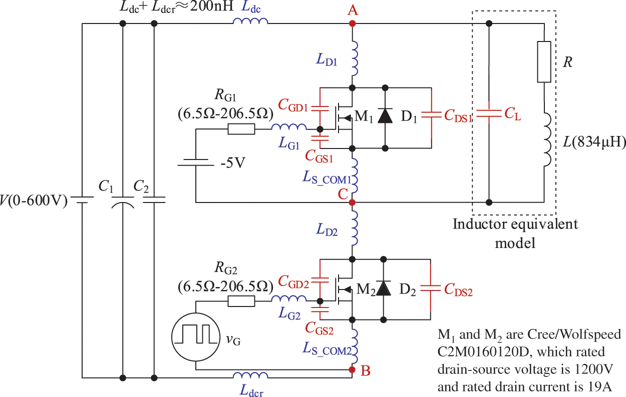
Figure 1: Schematic diagram of the DPT circuit
The driver voltage vG is a double-pulse signal, which is shown in Fig. 2. The low voltage of the double-pulse signal is about −5 V to ensure the SiC MOSFET turned off reliably. The high voltage of the double-pulse signal often exceeds 20 V to make the SiC MOSFET turned on fully. At the falling edge of the first pulse, the circuit state when the SiC MOSFET M2 turns off can be tested. At the rising edge of the second pulse, the circuit state when the SiC MOSFET M2 turns on can be tested.
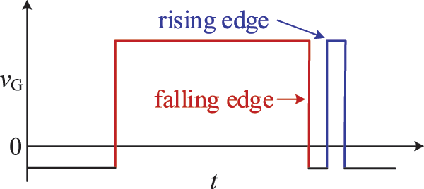
Figure 2: Double pulse signal
2.2 Circuit Analysis When M2 Turns on
When M2 is on a stable off-state or a stable on-state, the circuit can operate steadily no matter how large the parasitic inductance in the circuit is. These processes are the same as those of the Si IGBT converter.
When M2 is turned on, the equivalent circuit model at this time is shown in Fig. 3. The Coss1 is the output capacitance of M1 and Coss2 is the output capacitance of M2. Note that the value of Coss1 is the sum of CDS1 and CGD1 and the value of Coss2 is the sum of CDS2 and CGD2. Ron is the equivalent variable resistance of M2 when it switches.
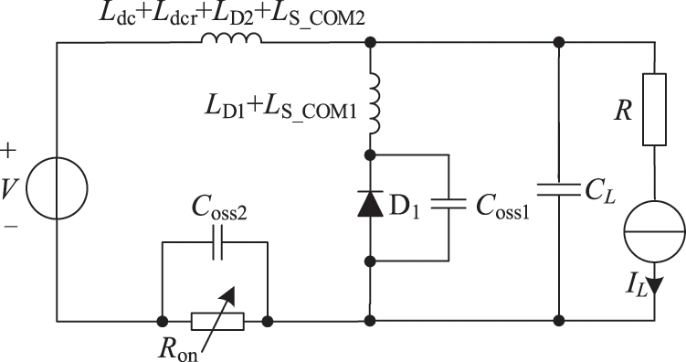
Figure 3: Equivalent model of the current flow path at the falling edge of the first pulse or at the rising edge of the second pulse
Because the switch speed of the SiC MOSFET is extremely fast, the series circuit of the DC voltage source V and the variable resistance Ron can be equivalent to a step voltage source Vs. The equivalent model in Fig. 3 can be simplified as shown in Fig. 4a. According to the superposition theorem, the circuit can be disassembled into two sub circuits, which are shown in Figs. 4b and 4c, respectively.
From Fig. 4, when the oscillation is caused by the equivalent step voltage, the parasitic inductance and the output capacitance will occur in the circuit. The voltage across Coss1 can be calculated by
where Ltotal is the sum of Ldc, Ldcr, LD1, LD2, LS_COM1 and LS_COM2. This means that due to the extremely fast switching speed of the SiC MOSFET, the oscillation amplitude will reach twice the DC bus-bar voltage. Note that the oscillation will be very small when the Si IGBT is used because its switching speed is very slow and Vs can only be regarded as a ramp signal not a step signal.
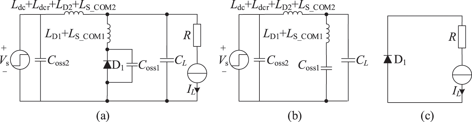
Figure 4: Simplified model of the current flow path when M2 switches: (a) simplified model, (b) considering only the voltage source, and (c) considering only the current source
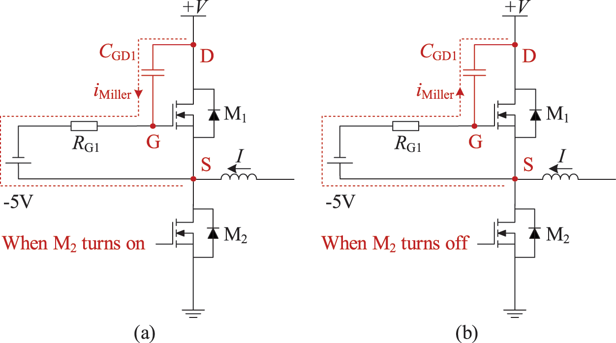
Figure 5: Cross-talk effect when M1 is OFF: (a) when M2 turns on, and (b) when M2 turns off [22]
Moreover, during the SiC MOSFET turning on, there is not only oscillation problem but also cross-talk problem, which can be explained by Fig. 5a. When the SiC MOSFET M2 turns on, the drain-source voltage across M1 increases rapidly and the current iMiller through the Miller capacitance CGD1 will be generated. The current iMiller will induce a positive voltage on the gate of M1. As the switching speed of M2 gradually increases, the iMiller will be large and then the gate voltage of M1 may exceed the threshold value. M1 will turn on falsely and the shoot-through failure will happen.
Considering the oscillation problem mentioned above, iMiller will contain a huge oscillation so the gate voltage will have a very serious oscillation problem.
2.3 Circuit Analysis When M2 Turns off
When M2 is turned off, the equivalent circuit is similar to that when it is turned on, which is shown in Figs. 4b and 4c. The difference is that the step signal is the negative step (V to 0) at this time. The voltage across Coss1 when M2 turns off can be calculated by
It means that the oscillations in the circuit will still exist when M2 turns off but the oscillation range is between -V to V. Similarly, the oscillations here will be much larger than those in the Si IGBT converter.
Moreover, during the turning off process of the M2, there is also cross-talk problem, which can be explained by Fig. 5b. When M2 turns off, the drain-source voltage across M1 decreases rapidly and the current iMiller through the Miller capacitance CGD1 will be generated. The current iMiller will induce a negative voltage on the gate of M1. The introduced negative voltage needs to be constrained, otherwise there is a risk of breaking through the gate oxide of M1. Compared to the turn-on process, there is no shoot-through problem and the severity is smaller to some extent.
3 Function of the Ferrite Bead in the Main Circuit
To replace the Si IGBT with the SiC MOSFET directly in the traditional power electronics converter, the problems of the huge oscillation and the cross-talk mentioned above must be solved. This paper presents a method of using the ferrite bead to solve the above problems and the effect of the ferrite bead is analyzed following.
The ferrite bead is essentially a single-coil inductor which has great damping effect at a certain frequency range. The equivalent model of the ferrite bead is shown in Fig. 6. LFB is the equivalent inductance of the ferrite bead. CFB is the equivalent capacitance of the ferrite bead. RFB1 and RFB2 are the equivalent resistances of the ferrite bead.
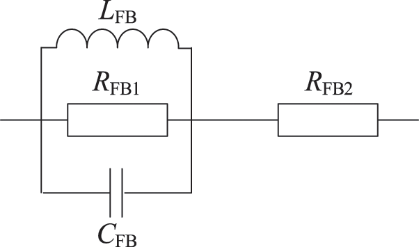
Figure 6: Equivalent model of the ferrite bead
The impedance expression of the ferrite bead can be given by
where ω is the angular frequency and the other parameters can be expressed by
From the formula, it can be found that the ferrite bead can finally be equivalent to a series circuit of the inductance and the resistance, and the equivalent resistance and the inductance vary with the change of the frequency.
Fig. 7 gives the measured impedance characteristic curves of a common ferrite bead. The total inductance of the ferrite bead decreases with the increase of the frequency, and the total resistance of the ferrite bead increases with the increase of the frequency.
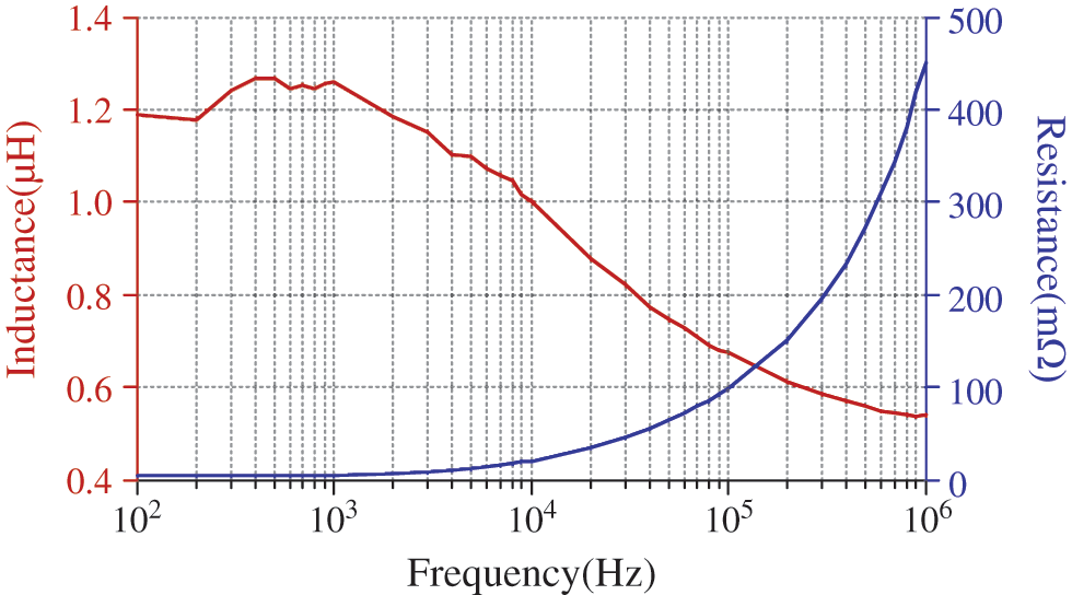
Figure 7: Measured impedance characteristic curves of a common ferrite bead
The analysis above means that the ferrite bead exhibits the inductance characteristic at the low frequency and the resistance characteristic at the high frequency. This property of the ferrite bead can be used to dampen the large high frequency oscillations of the circuit mentioned in Section 2 and has little effect on the normal switch waveforms during the SiC MOSFET switching.
3.2 Inhibition of Oscillation by the Ferrite Bead
To suppress the main circuit oscillation during the switching process of M2, the ferrite bead can be added in the main circuit, which is shown in Fig. 8, where FB is the added ferrite bead.
After the ferrite bead is inserted into the main circuit, it is necessary to analyze the non-oscillation component and the oscillation component respectively. For the non-oscillation component, the inductance in the circuit when M2 turns on can be considered as a wire and the ferrite bead can be equivalent to a wire too. The simplified circuit model considering only the voltage source at this time can be shown in Fig. 9a, in which case the ferrite bead has no effect on the main circuit.
For the oscillation component, the ferrite bead can be equivalent to a resistance. The simplified circuit model considering only the voltage source at this time can be shown in Fig. 9b. When the M2 turns on, the voltage across Coss1 is a damped or the overdamped oscillation waveform. If it is a damped oscillation, the overshoot is
where
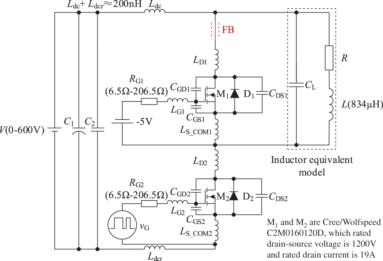
Figure 8: Ferrite bead position when M2 switched
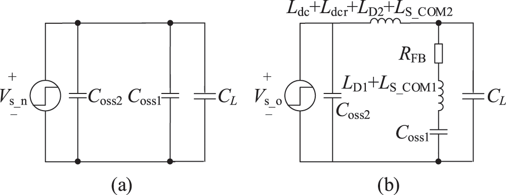
Figure 9: Simplified model considering only the voltage source: (a) for the non-oscillation component, and (b) for the oscillation component
Because of the resistance of the ferrite bead at the oscillation frequency, the oscillation in the equipment circuit can be effectively suppressed when the Si IGBT is replaced by the SiC MOSFET.
Note that when M2 is turned off, the current load will be in the ferrite bead, which will saturate the ferrite bead, in which case the ferrite bead has no influence on the oscillation problem during the turning off process in the DPT circuit. However, in practical converters, the ferrite beads can be added to the upper and the lower SiC MOSFETs of the half bridge, and the oscillation can be suppressed by the ferrite bead in series with the complementary device when it turns off.
3.3 Inhibition of Cross-Talk by the Ferrite Bead
The cross-talk is influenced by the ferrite bead, which is discussed as follows:
When M2 turns on, the cross-talk after the ferrite bead being inserted can be shown in Fig. 10a. Since the ferrite bead can be equivalent to a series circuit of resistance and inductance, the ferrite bead will reduce the Miller current iMiller and the value of gate-source voltage of M1. Therefore, the shoot-through risk will be reduced greatly. Note that when M2 turns on, the current will completely convert from M1 to M2, and then the drain-source voltage of M1 will rise, thus there is no saturation problem of the ferrite bead at this cross-talk process.
When M2 turns off, the cross-talk after the ferrite bead being inserted can be shown in Fig. 10b. The ferrite bead will reduce the Miller current iMiller and the gate-source voltage of M1. Therefore, the risk of breaking through the gate oxide will be reduced. Note that when the M2 turns off, the drain-source voltage of M1 will fall firstly, and the current will convert from M2 to M1, thus there is no saturation problem of the ferrite bead at this cross-talk process.
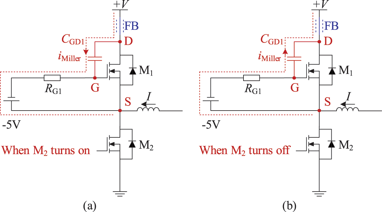
Figure 10: Cross-talk effect after the ferrite bead inserted: (a) when M2 turns on, and (b) when M2 turns off
The picture of the double-pulse test platform is shown in Fig. 11. The schematic diagram is shown in Figs. 1 and 8, and the position of the ferrite bead is shown by the FB in Fig. 8. The parameters of devices are listed in the two figures. About the installation method of the ferrite bead, it is directly welded to the drain pin of the SiC MOSFET M1, and both of them in combination are welded to the circuit board. In the experimental platform, the C2M0160120D from Cree/Wolfspeed is chosen as the SiC MOSFET M1 and M2, whose rated voltage is 1200 V and rated current is 19 A. The DC voltage source can be adjusted from 0 V to 600 V. The load is the self-made air-core inductor, which can avoid the saturated load inductance. The inductance value of it is 834 μH. Because the experiment is to demonstrate the application of SiC MOSFETs in the main circuit which is suitable to Si IGBTs, the parasitic inductance of the main circuit Ldc+Ldcr approximates 200 nH. Considering that the internal drive resistance of M1 and M2 is 6.5 Ω, the adjustment ranges of the total driver resistor RG1 and RG2 are 6.5 Ω to 206.5 Ω. Due to the fast switching speed of the SiC MOSFET and the high oscillation frequency of the circuit, the bandwidth of the oscilloscope, the voltage probes and the current probe are 100 MHz, 100 MHz and 120 MHz respectively. Further, in order to use more points to represent the ns level waveform, the sampling rate of the selected oscilloscope is 2.5 GS/s.
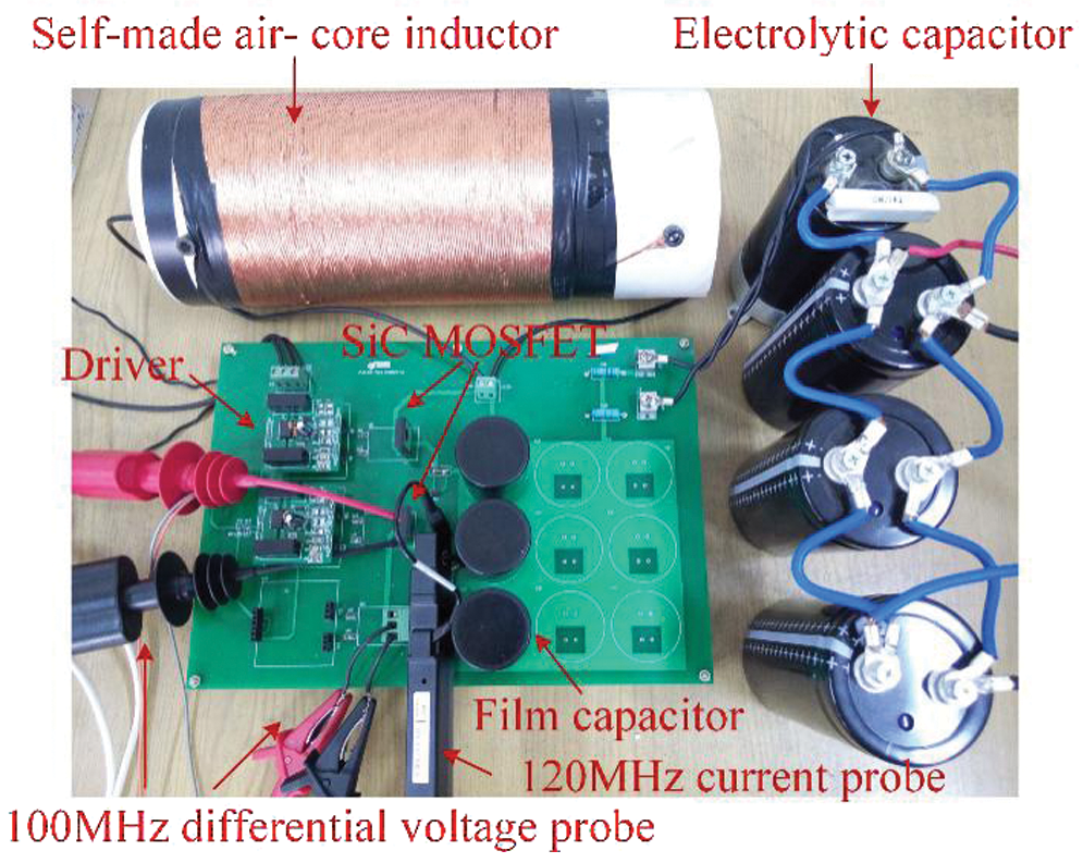
Figure 11: Experimental platform
The traditional Si IGBT converter often has large parasitic parameters in the hardware, which is also the reason why the converter cannot work when the Si IGBT is directly replaced by the SiC MOSFET. In order to study this problem, the experimental platform in this paper is designed to simulate the situation with the large parasitic inductance in the traditional Si IGBT converter. Using the method proposed in this paper, the Si IGBT can be replaced by the SiC MOSFET without redesigning the circuit of the traditional Si IGBT converter to improve the efficiency of the converter.
4.2 Oscillation Waveform without the Ferrite Bead
Due to the huge parasitic inductance in the main circuit when the Si IGBT was directly replaced by the SiC MOSFET, the voltage and the current in the circuit will oscillate seriously. Due to the influence of the shoot-through, the oscillations will be more serious when the SiC MOSFET turns on. When the DC voltage source is 88 V and the driver resistance is 26.5 Ω in the experiment, the huge oscillation phenomena will occur in the circuit. The waveforms of the DC bus-bar voltage, the driver supply voltage, the driver input signal (the controller output signal), the drain voltage, the drain current and the gate-source voltage of the M2 are shown in the Fig. 12. In the Figure, V is the DC bus-bar voltage of the double-pulse test platform; Vdriver_supply is the driver supply voltage of M2; Vsignal is the driver input signal of M2 and it is also the controller output signal for M2; VDS is the drain-source voltage of M2; iD is the drain current of M2; vGS is the gate-source voltage of M2. Note that the meanings of these symbols apply to all the figures below.
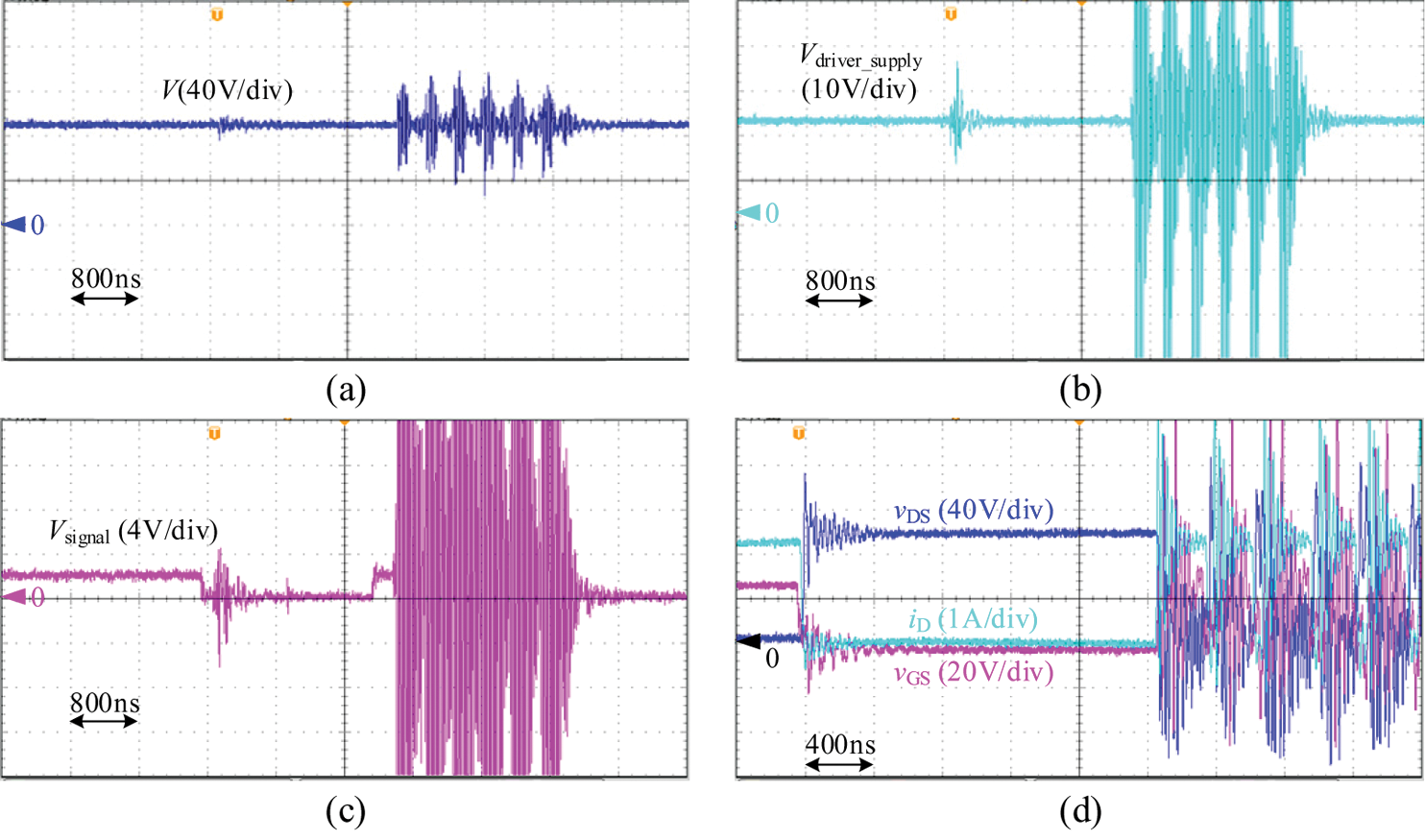
Figure 12: Oscillation waveform without the ferrite bead: (a) DC bus-bar voltage, (b) driver supply voltage, (c) driver input signal (the controller output signal), and (d) drain-source voltage, the drain current and the gate-source voltage of the M2
It can be seen from the Fig. 12 that the circuit can no longer work normally, and the corresponding waveforms are consistent with the above analysis. Due to the parasitic oscillation of the main circuit, the driver supply voltage and the controller output signal are also subjected to a huge EMI effect. Thus, the circuit will not work when the SiC MOSFET is used directly without taking any action. Note that the oscillation problem is much more serious when M2 is turned on than when it is turned off. This is because the shoot-through problem caused by the cross-talk when M2 is turned on will further aggravate the oscillation.
The oscillation can be reduced by lowering the DC bus-bar voltage. When the DC bus-bar voltage drops to 28 V, although the waveforms still oscillate, the oscillation can be attenuated and the circuit can work normally, as shown in Fig. 13. This is because when the DC bus-bar voltage decreases, the output capacitance of M2 will increase and its switching speed will slow down. Vs in the above analysis cannot be equivalent to a step signal, but can only be equivalent to a ramp signal, so the oscillation amplitude decreases. Moreover, in the situation of the reduced DC bus voltage, the shoot-through energy decreases when the cross-talk occurs, and the negative impact of the shoot-through problem on the oscillation is relieved.
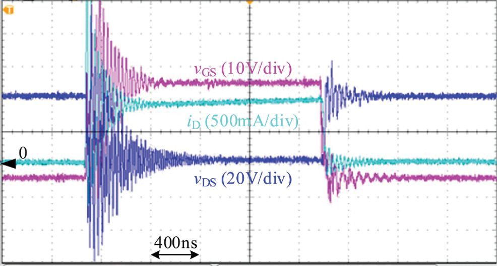
Figure 13: Waveform of M2 when the DC bus-bar voltage is low
Certainly, it is not desirable to operate a 1200 V SiC MOSFET at the 28 V DC bus-bar voltage, and it does not satisfy the use requirement of the SiC MOSFET in the traditional Si IGBT converter. Thus, a method must be found for the circuit to work at the high DC bus-bar voltage.
4.3 Oscillation Suppression Method of Regulating the Driver Resistance
According to the above analysis, when the switching speed of the SiC MOSFET decreases, the oscillation problem will be alleviated. The switching speed of the SiC MOSFET can be reduced by increasing the driver resistance. In order to make the circuit work properly at the DC bus-bar voltage of 600 V, the driver resistance of M2 is set as 206.5 Ω. The drain-source voltage, the drain current and the instantaneous loss power of M2 when it turns on and turns off are shown in Fig. 14. The oscillation is attenuated and the circuit works normally. ps is the power loss when M2 turns on or turns off. The definition of ps also applies to the following formulas and figures.
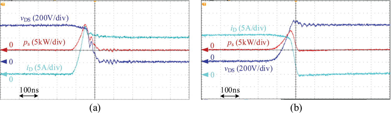
Figure 14: The drain-source voltage, the drain current and the instantaneous loss power of M2 at the DC bus-bar voltage of 600 V and the driver resistance of 206.5 Ω: (a) when it turns on, and (b) when it turns off
In this situation, the turn-on and turn-off time of the SiC MOSFET is slightly more than 100 ns. The switching loss can be obtained by
where Eon is the turn-on loss; Eoff is the turn-off loss; t1 is the moment when the drain current begins to rise; t2 is the moment when the drain-source voltage finishes falling; t3 is the moment when the drain-source voltage begins to rise; t4 is the moment when the drain current finishes falling. Through calculation, the turn-on loss of M2 is 600 μJ, and the turn-off loss is 400 μJ. Note that although the switching time and the switching loss of the SiC MOSFET at this time do not reach the minimum value that can be achieved, the SiC MOSFET still has the advantage because the switching time and the switching loss are much smaller compared with those of the Si IGBT at the same power level.
The switching loss of the SiC MOSFET is related to the charging and the discharging time of the input capacitance of the SiC MOSFET. The longer the charging and discharging time is, the greater the loss is. The charging and discharging time depends on the gate turn-on resistance and gate turn-off resistance respectively. The turn-on loss and the turn-off loss can be regulated respectively by adjusting the gate turn-on resistance and the gate turn-off resistance. Since there is no shoot-through problem during the turn-off process of the SiC MOSFET, the oscillation is relatively small, which is also verified by the above experiments. Therefore, in order to reduce the switching loss of the SiC MOSFET, the gate turn-off resistance can be appropriately reduced to speed up the turn-off time, which will not lead to serious oscillation at the turn-off process of the SiC MOSFET.
When the turn-on gate resistance is 206.5 Ω and the turn-off gate resistance is 16 Ω, 24.7 Ω and 106.5 Ω respectively, the switching waveforms are shown in Fig. 15. In Fig. 15, the dark blue waveform is the drain-source voltage of M2, the light blue waveform is the drain current of M2, and the red waveform is the instantaneous loss power of M2.
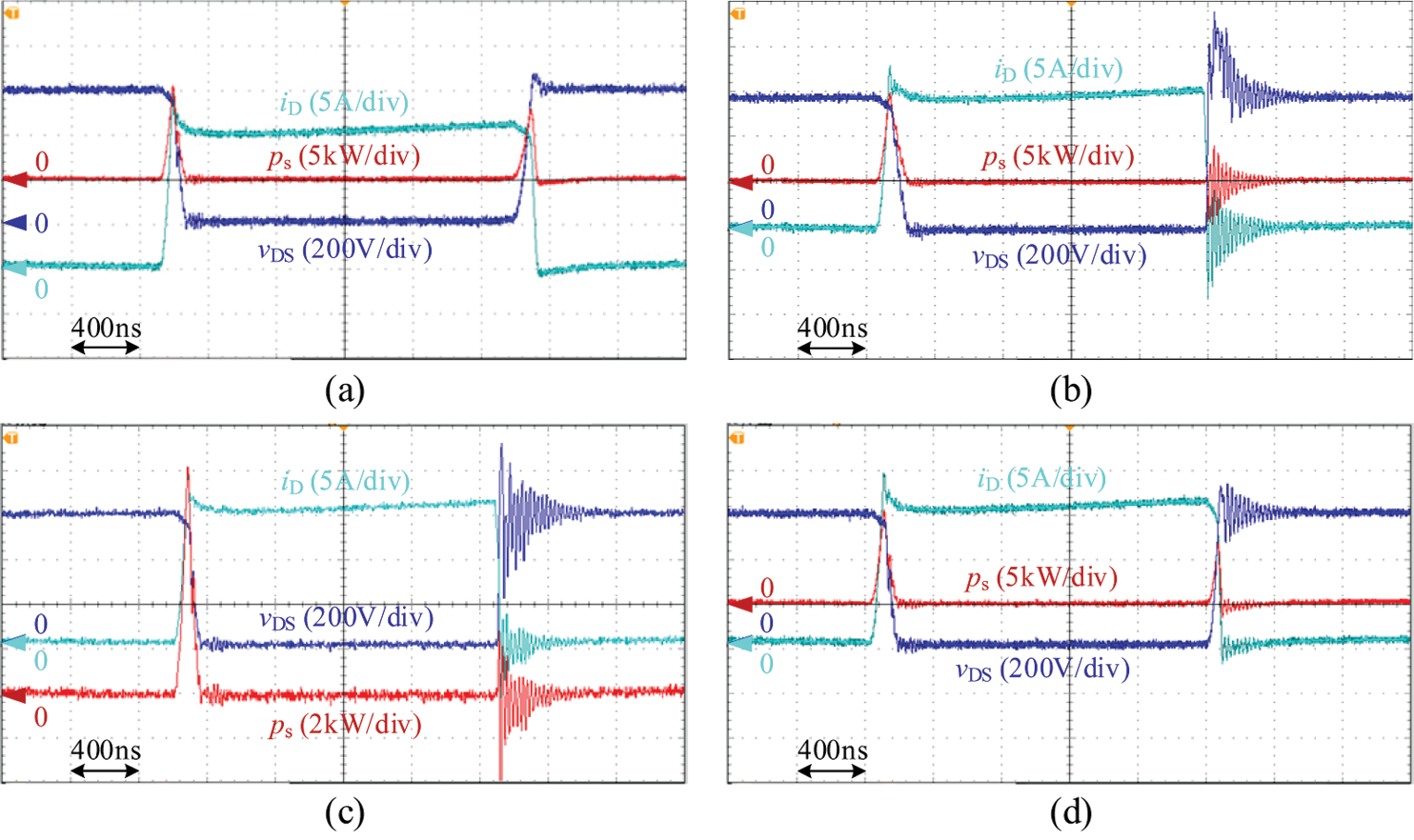
Figure 15: Switching waveforms of M2 at different turn-off gate resistance: (a) 206.5 Ω, (b) 16 Ω, (c) 24.7 Ω, and (d) 106.5 Ω
When the turn-off gate resistance is 16 Ω or 24.7 Ω, the turn-off oscillation is too large, affecting the normal work of the circuit. When the turn-off gate resistance is 106.5 Ω, the turn-off oscillation is moderate. The detailed switching processes of M2 are shown in Fig. 16. Through calculation, the turn-on loss is 600 μJ, and the turn-off loss is 320 μJ. The turn-on loss is the same as the above situation, and the turn-off loss is only the 80% of above situation, which means that decrease the turn-off gate resistance can reduce the turn-off loss on the premise of the less turn-on oscillation. Adopting this method, both the oscillation and the turn-off loss can be reduced to some extent, but the loss at the turn-on process cannot be reduced due to the big turn-on resistance.
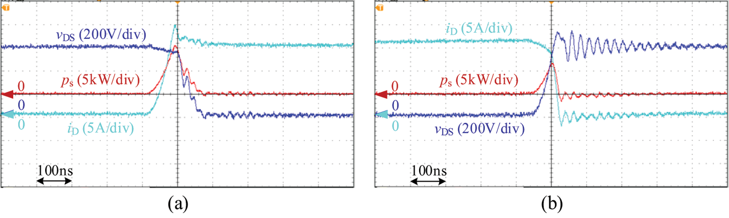
Figure 16: Detailed switching processes of M2 when the turn-on gate resistance is 206.5 Ω and the turn off gate resistance is 106.5 Ω: (a) turn-on waveforms, and (b) turn-off waveforms
Note that a gate resistance value around 200 Ω does not exist in practical applications because of the huge switching losses. The experiment of 206.5 Ω gate resistance in this paper is also set up to prove this point. In order to replace the Si IGBT with the SiC MOSFET to upgrade the converter without redesigning the circuit hardware structure, the first problem to be solved is the severe oscillation caused by the huge parasitic inductance. In order to reduce the severe oscillation, making the circuit work normally under the rated voltage, the traditional approach is to increase the gate resistance, but through the test of this paper, the resistance need to be increased to a very large value, such as 206.5 Ω. This is not practical, so this paper proposes a new method that inserts a ferrite bead in the main circuit to suppress the severe oscillation, which will be discussed below.
4.4 Oscillation Suppression Method of Inserting the Ferrite Bead in the Circuit
Inhibiting the circuit oscillation by increasing the driver resistance will inevitably increase the switching loss of the circuit, which will greatly reduce the advantage brought by the SiC MOSFET, so it is not a desirable solution. According to the above analysis, the ferrite bead can have a good damping effect on the high frequency electric quantity and it has no obvious effect on the switching speed of the SiC MOSFET. Thus, the ferrite bead can be used to reduce the oscillation without increasing the switching loss.
In the experiment, the ferrite beads are placed in the position shown in Fig. 8. Since the ferrite bead mainly play a large role in the oscillation during turn-on process of the M2, in order to reduce the turn-on loss, the turn-on gate resistance and the turn-off gate resistance in the experiment are 26.5 Ω and 106.5 Ω respectively. The switching waveforms of M2 at this time are shown in Fig. 17.
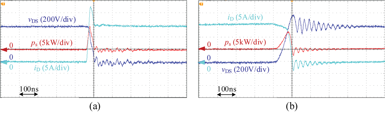
Figure 17: Switching waveforms of M2 after the ferrite bead inserted: (a) turn-on waveforms; (b) turn-off waveforms
It can be found from Fig. 17 that the oscillation during the turn-on process is almost completely eliminated even if the turn-on resistance is only 20 Ω, which does not work properly at all before the ferrite bead is inserted. According to the calculation, the turn-on loss of M2 is 280 μJ, and the turn-off loss of M2 is 400 μJ. Compared to the above switching loss without the ferrite bead when the turn-on gate resistance is 206.5 Ω and turn-off gate resistance is 106.5 Ω, the turn-on loss is decreased by 320 μJ (53%) and the turn-off loss is increased by 80 μJ (25%). The increase of the turn-off loss is due to the effect of the ferrite bead on the turn-off speed. However, since the ferrite bead can reduce the allowed turn-on gate resistance, the total switching loss is still reduced by 240 μJ (26%) after the ferrite bead is adopted on the premise of ensuring a small oscillation in the circuit. Thus, the ferrite bead ensures that the oscillation and the switching loss are both small when the Si IGBT in the conventional power electronics equipment is replaced by the SiC MOSFET.
Due to the influence of parasitic parameters in the traditional power electronics converter suitable for the Si IGBT, a serious circuit oscillation problem will occur when the Si IGBT is directly replaced by the SiC MOSFET. In this paper, the oscillation model with the adoption of the SiC MOSFET is established in the double-pulse test circuit and compared with the oscillation model after the ferrite bead being inserted in the main circuit. It is found that the ferrite bead has a good damping effect on the high-frequency oscillation and can relieve the cross-talk problem in the circuit. Through experiments, the three methods to suppress the oscillation are compared: Adopting the large driver resistance, the large turn-on gate resistance combined with the smaller turn-off gate resistance, and the ferrite bead combined with the smaller driver resistance. The last method can not only effectively suppress the oscillation, but also give full play to the advantage of small switching loss brought by the SiC MOSFET. Thus, to replace the Si IGBT in the traditional converter with the SiC MOSFET without redesigning the circuit, the ferrite bead can be inserted in the main circuit.
Funding Statement: This work was supported in part by the Natural Science Foundation of Jiangsu Province under Grant BK20200969 (L. Z., URL: http://std.jiangsu.gov.cn/), and in part by Nantong Science and Technology Plan Project under Grant JC2019095 (L. R., URL: http://kjj.nantong.gov.cn/)
Conflicts of Interest: The authors declare that they have no conflicts of interest to report regarding the present study.
1. Chen, Z., Yao, Y., Boroyevich, D., Ngo, K. D. T., Mattavelli, P. et al. (2014). A 1200-V, 60-A SiC MOSFET multichip phase-leg module for high-temperature, high-frequency applications. IEEE Transactions on Power Electronics, 29(5), 2307–2320. DOI 10.1109/TPEL.2013.2283245. [Google Scholar] [CrossRef]
2. Zhong, X., Wu, X., Zhou, W., Sheng, K. (2014). An all-SiC high-frequency boost DC-DC converter operating at 320°C junction temperature. IEEE Transactions on Power Electronics, 29(10), 5091–5096. DOI 10.1109/TPEL.2014.2311800. [Google Scholar] [CrossRef]
3. Hazra, S., De, A., Cheng, L., Palmour, J., Schupbach, M. et al. (2016). High switching performance of 1700 V, 50 A SiC power MOSFET over Si IGBT/BiMOSFET for advanced power conversion applications. IEEE Transactions on Power Electronics, 31(7), 4742–4754. DOI 10.1109/TPEL.2015.2432012. [Google Scholar] [CrossRef]
4. Palmour, J. W., Cheng, L., Pala, V., Brunt, E. V., Lichtenwalner, D. J. et al. (2014). Silicon carbide power MOSFETs: Breakthrough performance from 900 V up to 15 kV. 2014 IEEE 26th International Symposium on Power Semiconductor Devices & IC’s (ISPSD), pp. 79–82. Waikoloa, HI, USA. [Google Scholar]
5. Zhang, H., Tolbert, L. M. (2011). Efficiency impact of silicon carbide power electronics for modern wind turbine full scale frequency converter. IEEE Transactions on Industrial Electronics, 58(1), 21–28. DOI 10.1109/TIE.2010.2048292. [Google Scholar] [CrossRef]
6. Whitaker, B., Barkley, A., Cole, Z., Passmore, B., Martin, D. et al. (2014). A high-density, high-efficiency, isolated on-board vehicle battery charger utilizing silicon carbide power devices. IEEE Transactions on Power Electronics, 29(5), 2606–2617. DOI 10.1109/TPEL.2013.2279950. [Google Scholar] [CrossRef]
7. Bertelshofer, T., Horff, R., Maerz, A. (2016). A performance comparison of a 650 V Si IGBT and SiC MOSFET inverter under automotive conditions. Proceeding of PCIM, pp. 653–660, Nuremberg, Germany. [Google Scholar]
8. Doustad, D., Ameziani, M., Lhotellier, D., Lefebvre, S., Petit, M. (2017). Estimation of the losses in Si and SiC power modules for automotive applications. Proceeding of PCIM, pp. 1814–1821, Nuremberg, Germany. [Google Scholar]
9. Zeng, C., Li, Z., Yuan, F., Jiang, X., He, Z. et al. (2018). Comparison of SiC synchronous rectification and schottky diode in voltage source inverters. 2018 IEEE Energy Conversion Congress and Exposition, pp. 1903–1906. Portland, OR, USA. [Google Scholar]
10. Zhang, L., Yuan, X., Zhang, J., Wu, X., Zhang, Y. et al. (2019). Modeling and implementation of optimal asymmetric variable dead-time setting for SiC MOSFET-based three-phase two-level inverters. IEEE Transactions on Power Electronics, 34(12), 11645–11660. DOI 10.1109/TPEL.2019.2905882. [Google Scholar] [CrossRef]
11. Pitlini, R., Zhang, Z., Andersen, M. (2013). Switching performance evaluation of commercial SiC power devices (SiC JFET and SiC MOSFET) in relation to the gate driver complexity. Proceeding of IEEE ECCE Asia Downunder, pp. 233–239, Melbourne, VIC, Australia. [Google Scholar]
12. Cree/Wolfspeed (2015). Design considerations for designing with Cree SiC modules part 1. Understanding the effects of parasitic inductance. https://www.wolfspeed.com/downloads/dl/file/id/180/product/0/design_considerations_for_designing_with_cree_sic_modules_part_1_understanding_the_effects_of_parasitic_inductance.pdf. [Google Scholar]
13. Ke, J., Zhao, Z., Xie, Z., Wei, C., Sun, P. (2017). Modeling and simulation of SiC MOSFET turn-off oscillation under influence of parasitic parameter. Proceeding of 2017 Sixth Asia-Pacific Conference on Antennas and Propagation, Xi’an, China. [Google Scholar]
14. Cree/Wolfspeed (2015). Design considerations for designing with Cree SiC modules part 2. Techniques for minimizing parasitic inductance. https://www.wolfspeed.com/downloads/dl/file/id/181/product/0/design_considerations_for_designing_with_cree_sic_modules_part_2_techniques_for_minimizing_parasitic_inductance.pdf. [Google Scholar]
15. Li, H., Munk-Nielsen, S. (2014). Challenges in switching SiC MOSFET without ringing. Proceeding of Pcim Europe, International Exhibition & Conference for Power Electronics. VDE, pp. 1–6, Nuremberg, Germany. [Google Scholar]
16. Huang, H., Yang, X., Wen, Y., Long, Z. (2016). A switching ringing suppression scheme of SiC MOSFET by active gate drive. Proceeding of 2016 IEEE 8th International Power Electronics and Motion Control Conference (IPEMC 2016-ECCE Asia), pp. 285–291, Asia Hefei, China. [Google Scholar]
17. Kim, J., Shin, D., Sul, S. (2018). A damping scheme for switching ringing of full SiC MOSFET by air core PCB circuit. IEEE Transactions on Power Electronics, 33(6), 4605–4615. DOI 10.1109/TPEL.2017.2731861. [Google Scholar] [CrossRef]
18. Chen, Z., Amaro, I. (2012). Optimizing low side gate resistance for damping phase node ringing of synchronous buck converter. Proceeding of IEEE Energy Conversion Congress & Exposition, pp. 1827–1832, Raleigh, NC, USA. [Google Scholar]
19. Yatsugi, K., Nomura, K., Hattori, Y. (2018). Analytical technique for designing an RC snubber circuit for ringing suppression in a phase-leg configuration. IEEE Transactions on Power Electronics, 33(6), 4736–4745. DOI 10.1109/TPEL.2017.2731421. [Google Scholar] [CrossRef]
20. Chuai, G., Wang, J., Yuan, X., Lai, B., Zhang, Q. (2019). Design and parasitic parameters analysis of a LCC resonant inverter using SiC MOSFET. Proceeding of 2019 22nd International Conference on Electrical Machines and Systems, Harbin, China. [Google Scholar]
21. Liu, B., Li, W., Meng, D., Diao, L., Ma, Y. et al. (2020). Low-stray inductance optimized design for power circuit of SiC-MOSFET-based inverter. IEEE Access, 8, 20749–20758. DOI 10.1109/ACCESS.2020.2964687. [Google Scholar] [CrossRef]
22. Yatsugi, K., Oishi, K., Iizuka, H. (2021). Ringing suppression of SiC MOSFET using a strongly coupled external resonator through analogy with passive PT-symmetry. IEEE Transactions on Power Electronics, 36(3), 2964–2970. DOI 10.1109/TPEL.2020.3013399. [Google Scholar] [CrossRef]
23. Jahdi, S., Alatise, O., Gonzalez, J. A. O., Bonyadi, R., Ran, L. et al. (2016). Temperature and switching rate dependence of crosstalk in Si-IGBT and SiC power modules. IEEE Transactions on Industrial Electronics, 63(2), 849–863. DOI 10.1109/TIE.2015.2491880. [Google Scholar] [CrossRef]
24. Zhang, L., Yuan, X., Wu, X., Shi, C., Zhang, J. et al. (2019). Performance evaluation of high-power SiC MOSFET modules in comparison to Si IGBT modules. IEEE Transactions on Power Electronics, 34(2), 1181–1196. DOI 10.1109/TPEL.2018.2834345. [Google Scholar] [CrossRef]
25. Zhang, Z., Zhang, W., Wang, F., Tolbert, L. M., Blalock, B. J. (2012). Analysis of the switching speed limitation of wide band-gap devices in a phase-leg configuration. Proceeding of Energy Conversion Congress & Exposition, pp. 3950–3955, Raleigh, NC, USA. [Google Scholar]
26. Xu, S., Sun, W., Sun, D. (2010). Analysis and design optimization of brushless DC motor’s driving circuit considering the Cdv/dt induced Effect. Proceeding of 2010 IEEE Energy Conversion Congress and Exposition, pp. 2091–2095, Atlanta, GA, USA. [Google Scholar]
27. Li, H., Jiang, Y., Qiu, Z., Wang, Y., Ding, Y. (2021). A predictive algorithm for crosstalk peaks of SiC MOSFET by considering the nonlinearity of gate-drain capacitance. IEEE Transactions on Power Electronics, 36(3), 2823–2834. DOI 10.1109/TPEL.2020.3016155. [Google Scholar] [CrossRef]
28. Yin, S., Tseng, K. J., Tong, C. F., Simanjorang, R., Gajanayake, C. J. et al. (2015). Gate driver optimization to mitigate shoot-through in high-speed switching SiC half bridge module. IEEE 11th International Conference on Power Electronics and Drive Systems, pp. 484–491, Sydney, NSW, Australia. [Google Scholar]
29. Zhang, Z., Wang, F., Tolbert, L. M., Blalock, B. J. (2014). Active gate driver for crosstalk suppression of SiC devices in a phase-leg configuration. IEEE Transactions on Power Electronics, 29(4), 1986–1997. DOI 10.1109/TPEL.2013.2268058. [Google Scholar] [CrossRef]
30. Tang, H., Chung, H. S., Fan, J. W., Yeung, R. S., Lau, R. W. (2020). Passive resonant level shifter for suppression of crosstalk effect and reduction of body diode loss of SiC MOSFETs in bridge legs. IEEE Transactions on Power Electronics, 35(7), 7204–7225. DOI 10.1109/TPEL.2019.2957985. [Google Scholar] [CrossRef]
31. Li, C., Lu, Z., Chen, Y., Li, C., Luo, H. et al. (2020). High off-state impedance gate driver of SiC MOSFETs for crosstalk voltage elimination considering common-source inductance. IEEE Transactions on Power Electronics, 35(3), 2999–3011. DOI 10.1109/TPEL.2019.2932263. [Google Scholar] [CrossRef]
32. Zhang, B., Xie, S., Xu, J., Qian, Q., Zhang, Z. et al. (2017). A magnetic coupling based gate driver for crosstalk suppression of SiC MOSFETs. IEEE Transactions on Industrial Electronics, 64(11), 9052–9063. DOI 10.1109/TIE.2017.2736500. [Google Scholar] [CrossRef]
 | This work is licensed under a Creative Commons Attribution 4.0 International License, which permits unrestricted use, distribution, and reproduction in any medium, provided the original work is properly cited. |