DOI:10.32604/csse.2022.019106
| Computer Systems Science & Engineering DOI:10.32604/csse.2022.019106 | |
| Article |
Timing Error Aware Register Allocation in TS
1Information Science and Engineering Department, Hunan First Normal University, Changsha, 410205, China
2Computer School, Wuhan University, Wuhan, 430072, China
3Department of Computer Science, Kennesaw State University, Kennesaw, 30144-5588, USA
4Hunan Guangyi Experimental Middle School, Changsha, 410205, China
*Corresponding Author: Sheng Xiao. sxiao@hnfnu.edu.cn
Received: 02 April 2021; Accepted: 13 May 2021
Abstract: Timing speculative (TS) architecture is promising for improving the energy efficiency of microprocessors. Error recovery units, designed for tolerating occasional timing errors, have been used to support a wider range of voltage scaling, therefore to achieve a better energy efficiency. More specifically, the timing error rate, influenced mainly by data forwarding, is the bottleneck for voltage down-scaling in TS processors. In this paper, a new Timing Error Aware Register Allocation method is proposed. First, we designed the Dependency aware Interference Graph (DIG) construction to get the information of Read after Write (RAW) in programs. To build the construction, we get the disassemble code as input and suppose that there are unlimited registers, the same way as so-called virtual registers in many compilers. Then we change the disassemble codes to the SSA form for each basic block to make sure the registers are defined only once. Based on the DIG construction, registers were reallocated to eliminate the timing error, by loosening the RAW dependencies. We construct the DIG for each function of the program and sort the edge of DIG by an increasing weight order. Since a smaller weighted-edge value means that its owner nodes have more frequent access in instruction flows, we expect it in different registers with no read-write dependency. At the same time, we make sure that there are no additional new spill codes emerging in our algorithm to minimize the rate of spill code. A high rate of spill code will not only decrease the performance of the system but also increase the unexpected read-write dependency. Next, we reallocate the registers by weight order in turn to loosen the RAW dependencies. Furthermore, we use the NOP operation to pad the instructions with a minimal distance value of 2. Experiment results showed that the average distance of RAW dependencies was increased by over 20%.
Keywords: Timing error; timing speculative architecture; register allocation; energy efficiency
Energy efficiency is an important issue. A number of works in different aspects have been completed [1–4]. Recently, timing speculation (TS) architecture has been proposed to improve the energy efficiency of microprocessors [5]. The traditional design of worst-case assumption about circuit timing constraints and clock-frequency is dated. Instead, TS architecture is proposed with the expectation that timing errors could occasionally occur in the system. To ensure the proper function of the processor, TS processor was included in timing error detection. Recovery mechanisms such as enhanced latches, checker and recovery modules were also included so that errors could be dynamically flagged and recovered [5,6].With relaxed timing constraints, timing error detection and recovery mechanisms, TS processor can work with a lower supply voltage, leading to potentially improved energy efficiency. However, error recovery operations are highly energy-consuming in TS processors, and the error rate is the dominating factor on how low the voltage can be scaled down to. A reduction of timing errors is therefore critical to improve the energy efficiency of the TS processors.
Compiler is an important system software and numerous optimization schemes are employed to generate optimized code for different architectures. In our previous work [7], we used register reallocation to reduce the crosstalk which could save energy and enhance the security. Recently, compilation-based techniques for TS processors have been studied [8,9]. Hoang et al. used compiler transformation to replace long delay operations with faster ones, so that the number of timing errors was reduced [8]. In Sartori and Kumar’s work [9], the relationship between current compilation optimization and TS processor was evaluated. Their experiments showed that the closer the read-write dependency was, the more likely timing errors could occur.
In recent years, an abundant amount of work has been done to improve the performance of TS processors by reducing timing errors in hardware architecture. Ernst et al. [5] proposed to dynamically detect and recover the timing error. Greskamp et al. [6] designed a timing error tolerated architecture. They used a fast approximation version for critical components of processor for execution and use a coprocessor to detect and recover errors. Xin and Joseph used timing error prediction to avoid full recovery overhead of timing errors [10]. Greskamp et al. [11] designed a processor from the ground up for TS. They identified the most frequently-exercised critical paths in the design and sped them up so that the error rate increases much more slowly as frequency increases. Kahng et al. [12] proposed a power-aware slack redistribution to enable extended voltage/reliability tradeoffs in processors. Powell et al. [13] used hardware mechanisms to save and transfer state. Xun et al. [14] proposed CLIM, a cross-level workload-aware timing error prediction model for functional units(FUs). CLIM predicted whether there are timing errors in FU at two levels: bit-level and value-level. On average, CLIM exhibited 95 percent prediction accuracy at value-level, 97 percent at bit-level, and executed at a rate of 173 times faster than GLS. Rioux et al. [15] presented a solution to connect the model-checking tool ROMEO to the designed process, thus allowing the verification of the system timing behavior at early stages. In order to avoid aging-induced timing errors, Heba et al. [16] proposed a paradigm shift in designing guard-bands: to select the guard-band types on-the-fly with respect to the workload-induced temperatures, aiming at optimizing for performance under temperature and reliability constraints. Ying et al. [17] proposed a novel timing analysis and frequency setting method for NN-based approximate computing circuits, based on in-field NN retraining. Their experimental results showed that timing errors in neural circuits could be effectively tamed for different applications, so that the circuits could operate at higher clocking rates under the specified quality constraint or be dynamically scaled to work at a wide range of frequency states with only minor accuracy losses.
There is also research from the software side that considers optimization for TS processors such as code transformation at the compiler level. Meixer et al. [18] used code transformation to avoid working in faulty processor components. Reddiet et al. [19] applied compiler optimization to reduce the stress on power delivery system. In Hari et al.’s work [20], the authors proposed a method of system-software guided detection of hard faults during processor lifetime. Hoang et al. observed that some code sequences could place greater demand on circuit timing deadlines than others. If these codes were selectively replaced with semantically equivalent instruction sequences which can reduce activity on timing critical circuit paths, fewer timing errors would be triggered, and thus recovery overhead could be reduced [8]. Sartori et al. [9] evaluated loop optimizations in compiler and also some other standard optimizations in GCC to show that significant energy benefits could be possible from TS-aware binary optimization.
In this paper, we propose a novel timing error aware register allocation method to reduce the energy consummation of TS architecture by reducing the distance of read-write dependencies: First, a heuristic register allocation method was designed to reschedule registers based on the distance of the read-write dependencies in each basic block. Then, an inter-block optimization algorithm was implemented to further increase the distance of read-write dependencies by considering the dependency between basic blocks. Experiment results showed that the proposed technique could increase the distance of read-write dependencies by 20% on average. Timing error could thus be reduced and an average energy saving ofapproximately15% could be achieved.
The primary contributions of the paper are as follows:
• Analyzes the distribution of RAW dependencies of the whole program and designed the Dependency aware Interference Graph (DIG) construction to express the relationship of RAW.
• Designs a heuristic register allocation method to break and increase the distance the RAW dependencies. As a result, the average distance of RAW is increased significantly.
• Implements the algorithm based on the GCC compiler. Experimental results verified that the average distance of RAW can be increased significantly. Error rate reduction leads to significantly energy saving by further voltage scaling.
The remainder of the paper is structured as follows: In Section 2, we introduce background information and a motivation example about the RAW reduction algorithm firstly. Then, the RAW dependencies optimization algorithm is described in detail. In Section 3, we present the evaluation methodology and the experimental results. The related work and conclusion are presented in Section 4 and Section 5, respectively.
Timing Speculation (TS) processor can improve the energy by more voltage scaling supporting. Razor [5] is typical TS processor. Razor relies on a combination of architectural and circuit level techniques for efficient error detection and correction of delay path failures. Each flip-flop in the design is augmented with a so-called shadow latch which is controlled by a delayed clock. The operation of a Razor flip flop is illustrated in Fig. 1 In clock cycle 1, the combinational logicL1 meets the setup time by the rising edge of the clock and both the main flip-flop and the shadow latch will latch the correct data. In this case, the error signal at the output of the XOR gate remains low and the operation of the pipeline is unaltered.
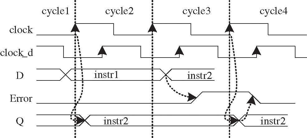
Figure 1: Pipeline augmented with razor latches and control lines
In cycle 2 in Fig. 1, we show an example of the operation when the combinational logic exceeds the intended delay due to sub-critical voltage scaling. In this case, the data is not latched by the main flip-flop, but since the shadow latch operates using a delayed clock, it successfully latches the data some time in cycle 3. To guarantee that the shadow latch will always latch the input data correctly, the allowable operating voltage is constrained at design time such that under worst-case conditions, the logic delay does not exceed the setup time of the shadow latch. By comparing the valid data of the shadow latch with the data in the main flip-flop, an error signal is then generated in cycle 3 and in the subsequent cycle, cycle 4, the valid data in the shadow latch is restored into the main flip-flop and becomes available to the next pipeline stage L2. Note that the local error signals Error_l are OR’ed together to ensure that the data in all flip-flops is restored even when only one of the Razor flip-flops generates an error.
If an error occurs in pipeline stage L1 in a particular clock cycle, the data in L2 in the following clock cycle is incorrect and must be flushed from the pipeline using one of the pipeline control methods such as clock gating, counter flow pipelining, and so on. However, since the shadow latch contains the correct output data of pipeline stage L1, the instruction does not need to be re-executed through this failing stage. Thus, a key feature of Razor is that if an instruction fails in a particular pipeline stage it is re-executed through the following pipeline stage, while incurring a one cycle penalty. The most of the proposed approaches therefore guarantee forward progress of a failing instruction, which is essential to avoid the perpetual failure of an instruction at a particular stage in the pipeline.
In addition to invalidating the data in the following pipeline stage, an error must also stall the preceding pipeline stages while the shadow latch data is restored into the main flip-flops. A number of different methods, such as clock gating or flushing the instruction in the preceding stages, were examined to accomplish this.
TS architecture is a promising concept for microprocessor energy efficiency. By using recovery mechanisms to tolerate the occasionally occurring timing errors, it can work in a lower supply voltage to obtain considerable energy saving. Recovery mechanisms are usually energy demanding in TS processors. Minimizing timing errors can significantly improve the energy efficiency of TS processor. As shown in the reference Sartori et al. [9], read-write dependencies in pipeline have a close relationship to timing errors for TS processors.
Read-write dependencies area common dependency in programs that break the pipelining and causes data hazard. Let instruction distance Dins(i,j) be the number of instructions between instruction
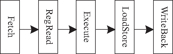
Figure 2: Pipeline of strongArm
The Read-write dependency will occur if and only if Eq. (1) is satisfied.
2.3 Timing Error Aware Register Allocation
In order to achieve aggressive optimization for the whole program such as the library of system, we make our optimization process get the disassemble codes and the profiling results as inputs. Then DIG constructor is used to build the DIG from the disassemble codes and sets the weight of it. Finally, we make the DIGRR processor analyze the DIG to relocate the register and generate the optimized code. The outline of the process is presented in Fig. 3.
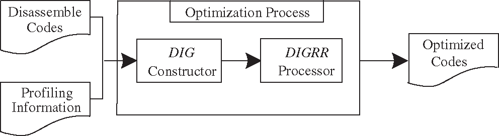
Figure 3: Outline of the optimization process
From this outline, we can see that the kernel of the optimization is DIG construction and DIGRR process, in the following two subsections, we will describe them in detail.
The goal of this work is to loosen the dependency of read-write operations in the TS processor. Therefore, the more frequently-accessed patterns of register pairs there are, the more important the register pairs are. For better illustration of the dependency accesses frequency feature, combined with the register allocation, we attempt to enhance the original Interference Graph that is widely used for register allocation and we construct the new dependency aware interference graph, called DIG.
DIG is a weighted undirected graph that can be represented by a four tuple
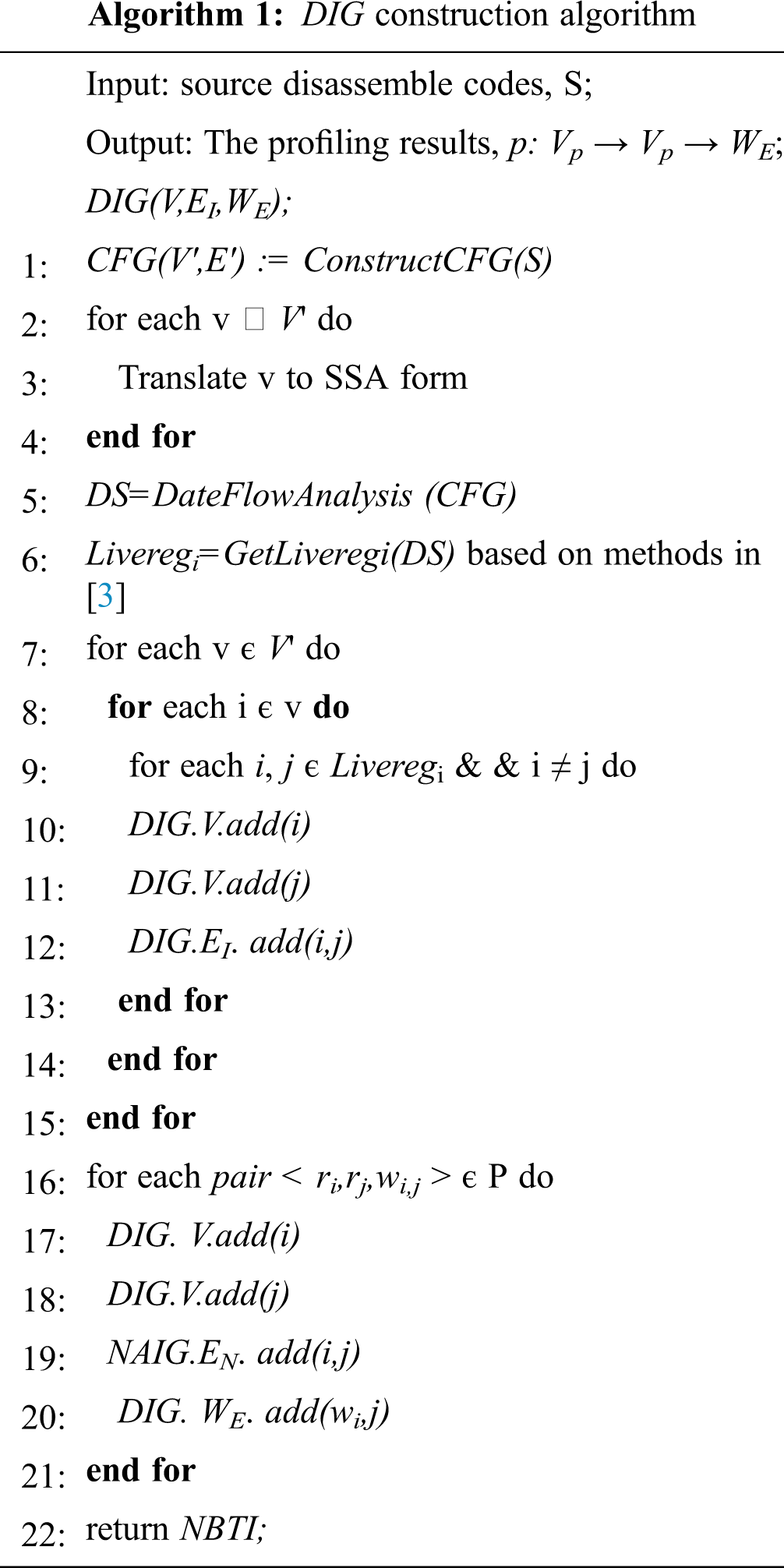
For building the DIG, we get the disassemble code as input and suppose that there are unlimited registers, the same as the registers called virtual registers in many compilers. First, we change the disassemble codes into the SSA form for each basic block that makes sure the registers are defined only once (line 1-4). Then, we use the methods described in the reference Liu et al. [3] to construct the data flow of each basic block and get the lifetime of each register in each instruction (line 5-6). The interference graph can be constructed with analysis of the live register in each instruction (line 7-15). After getting the interference graph, we can use the profiling results to add the weight of edges (line 16-21). And then we return the constructed DIG at last (line 22). The detailed construction algorithm is expressed in Algorithm 1. In Algorithm 1, the CFG is the control flow graph for the program and each node
To reduce the cost of a spill node is complex work because it changes the source order of instruction by inserting extra spill codes that will make the DIG rebuilt. Luckily, in our algorithm, we can avoid generating the spill codes since the source code is allocated successfully and we can always eliminate the spill code by assigning the spill node with its original one. The detailed reallocation algorithm is presented in next section.
Figs. 4a and 4b is the source instructions and the changed SSA representation respectively.
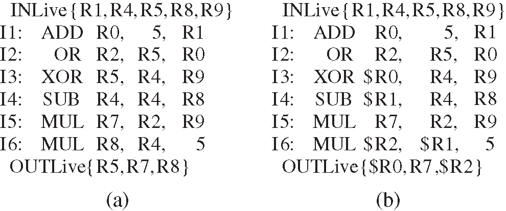
Figure 4: Example for SSA transforming (a) source code (b) SSA translation
2.3.2 DIG Based Timing Error Aware Register Reallocation (DIGRR)
Based on the above DIG, we implement our new DIG based Timing Error aware Register Reallocation (DIGRR) algorithm as follows. First, we construct the DIG for each function of the program 1. Then, we sort the edge of DIG by an increasing weight order (line 1). Since a smaller weighted-edge value means that its owner nodes have more frequently access in instruction flows, we expect it indifferent registers with no read-write dependency. At the same time, we expect to minimize the rate of spill code, of which a high rate will not only lose the performance of the system but also increase the unexpected read-write dependency, to make sure that no additional new spill codes will be emerged in our algorithm.
Then, we analyze the ordered edges one by one to finish the register allocation for each node (line 2-36). For each edge
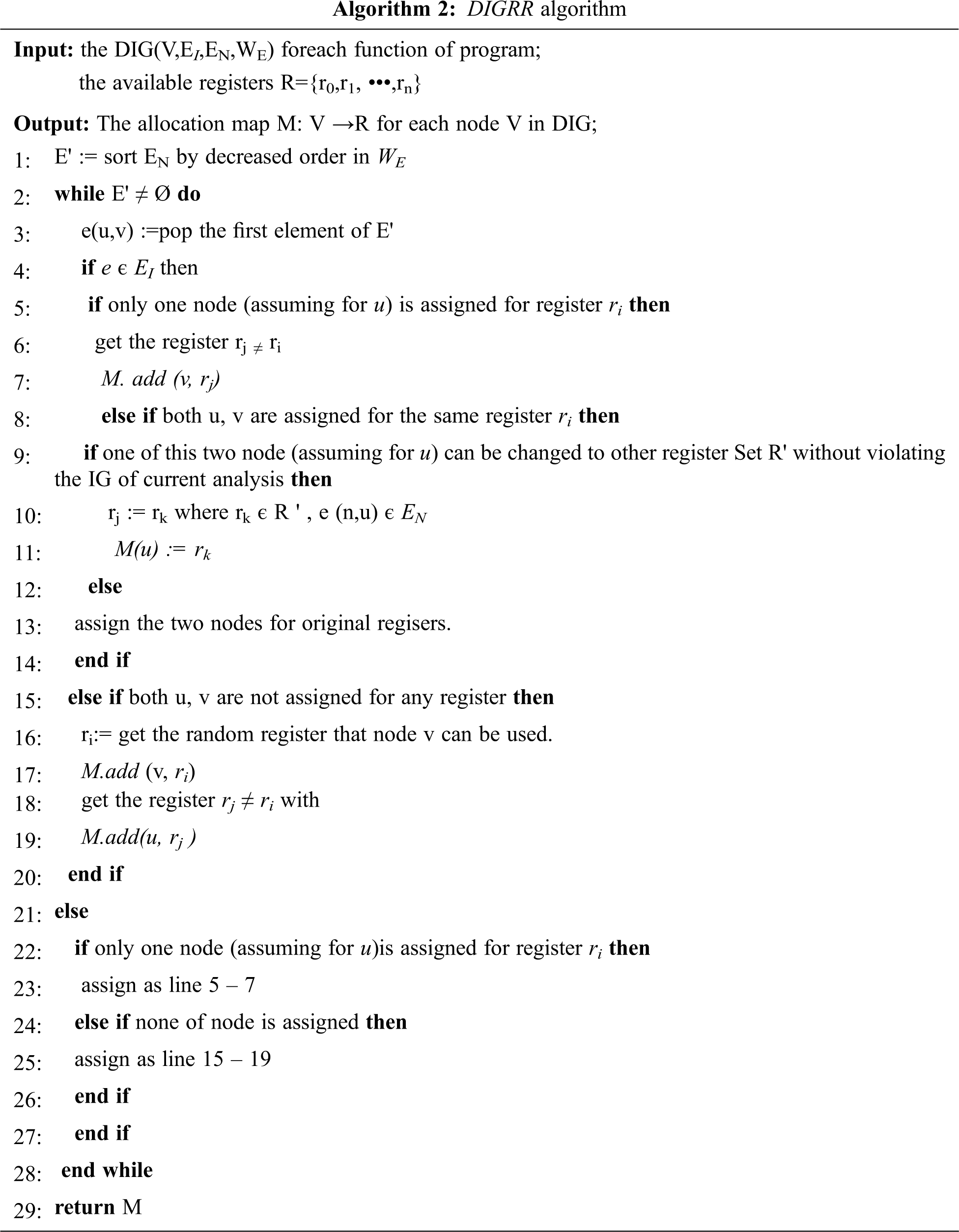
To further increase the distance of read-write dependency, we use the NOP operation to pad the instructions with a minimal distance value of 2.
Benchmarks from each category in Mibench [21] and Mediabench [22] are selected to evaluate the performance of the proposed algorithm. The target architecture is based on StrongARM. Arm-linux-gcc 4.4.3 is used as the base compiler. Obj-dump 2.19.51 is used to get the disassemble codes. The sim-profile tool for arm is used as profile tool to get the access frequency of instructions. The sim-profile in simplescalar arm tools is used as the base simulator. The static analysis method described in Wu et al. [23] is used to obtain the hot Read-write blocks and hot branches.The whole experimental framework is shown in Fig. 5.
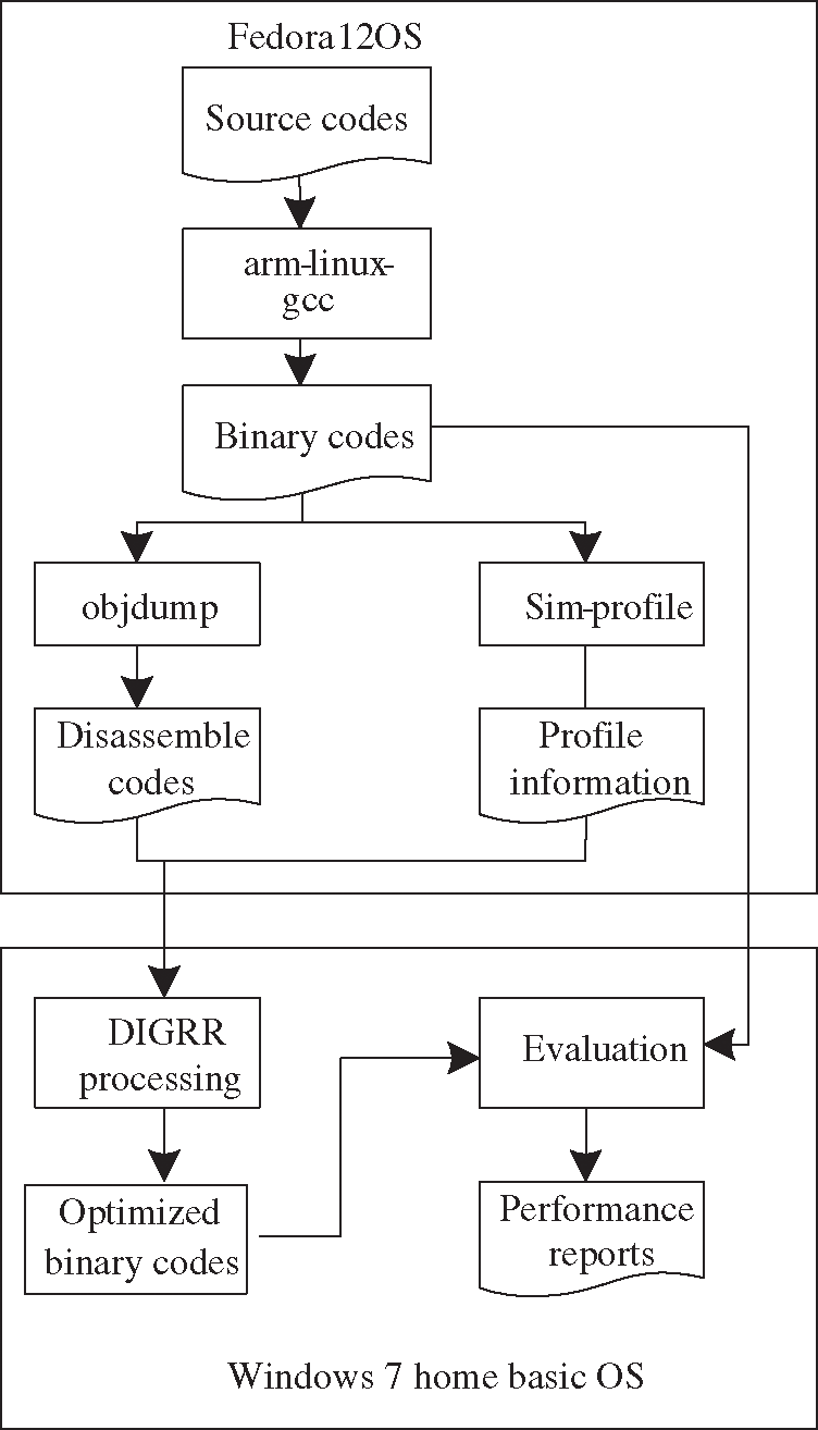
Figure 5: Experiment framework
In the experiments, the GCC compiler is modified by first obtaining the profiling information with O2 optimization option. Then, we disassemble and get profile information for the binary codes respectively. After getting the disassemble codes and profile information, we use them as input for the DIGRR processor to get the timing error aware optimized binary codes. Finally, we compare the source binary codes with the optimized binary codes to evaluate the performance of DIGRR from four aspects: the average distance of read-write dependency, the minimal distance of read-write dependency, the cost to get the minimal distance of read-write dependency, and the energy saving values.
To evaluate the effectiveness of the proposed algorithm in overall, we compared the average distance of the read-write dependency before and after DIGRR optimization. Fig. 6 shows the optimization result for the algorithm DIGRR. We normalize the results of optimization rate to the original GCC code.
3.2.1 The Average Distance of Read-write Dependency
The experiment result shows that we achieve, on average, up to 20% read-write reduction compared to the original GCC code. For some testing cases (such assusan_c_large, rijndael, sha, et al.) with a frequent use of registers, the optimization rate can reach up to more than 30%, which shows clearly the effectiveness of the algorithm in this paper. According to the relationship between error rate and scaled voltage as shown in Sartori et al. [9,24], a further voltage down-scaling can be achieved for better energy saving.
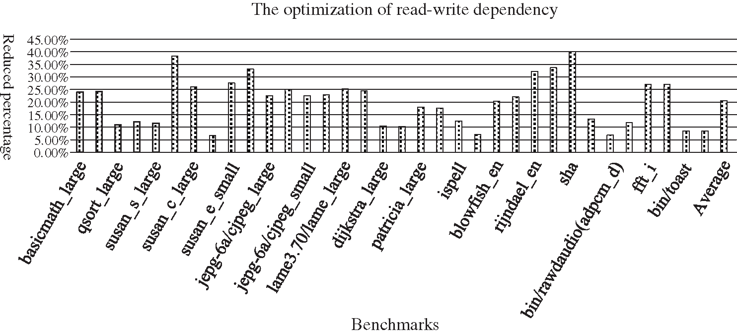
Figure 6: DF reduction results for GMS
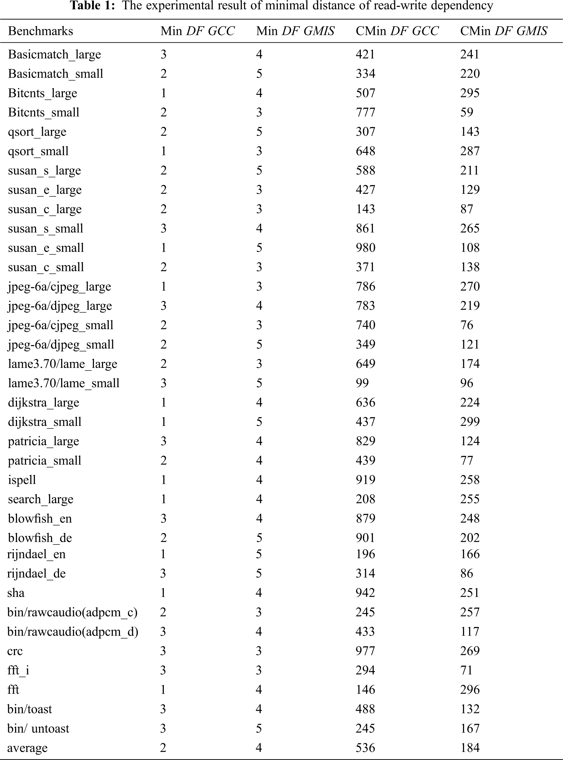
3.2.2 The Minimal Distance of Read-write Dependency
To evaluate the worst situation of our proposed algorithm, we compared the minimal distance value and its occurrence times obtained under GCC mode with those obtained under GMIS conditions. Tab. 1 shows the optimization results for the algorithm DIGRR. In the table, the first column lists the test case set, the second and third column represents the minimum distance of read-write dependency for GCC and GMIS, respectively. And the 4th and 5th column represents their occurrence times of the minimum distance of read-write dependency, respectively.
From the table, we can see that the minimum distance value of read-write dependency in GMIS is more than 2, and most of the individually-tested results are better under GMIS than under GGC (Tab. 1, column 3 vs. column 2).
It is obvious that the number of occurrence times for the minimum distance of read-write dependency is significantly reduced (Tab. 1, column 5 vs. column 4), the average occurrence times are reduced from 536 to 184, so the GMIS system also has a significant improvement for the worst-case scenario.
3.2.3 The Cost of Read-write Dependency
In order to increase the distance of read-write dependency, the NOP padding technology was used in our algorithm. Therefore, it could increase the time and space cost of the program to a certain extent. We conducted an evaluation of the increased costs. We used the original GCC code as the standard percentage base to evaluate the code after GMIS method optimization. The evaluation results are shown in Figs. 7 and 8.
From the experiment results, we can see that the timing cost and the space cost are both lowered. They are both about 0.5% on average. Therefore, the cost impact of our algorithm on the performance and size of the program is very small.
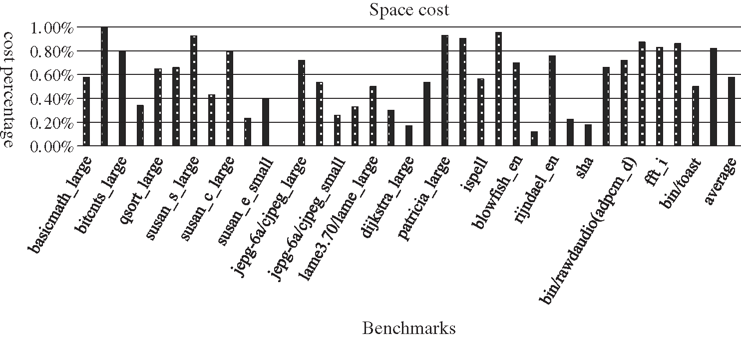
Figure 7: The space cost of DF reduction results for GMS
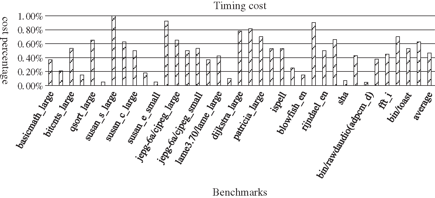
Figure 8: The timing cost of DF reduction results for GMS
3.2.4 The Energy Saving Values
In order to evaluate the impact of this method on the energy consumption of TS architecture processors, a comparative analysis of the code generated by GCC compilation and that obtained under the optimized conditions, was completed. From the experiment results shown in Fig. 9, we can see that the energy consumption of all programs has been reduced in a certain proportion. For some cases (such as susan_c_large, rijndael, sha, et al.), the energy consumption decreased by more than 20%, and the average energy consumption decreased by an approximate value of 16%. Therefore, it demonstrates in another aspect the effectiveness of this TS method for energy saving.
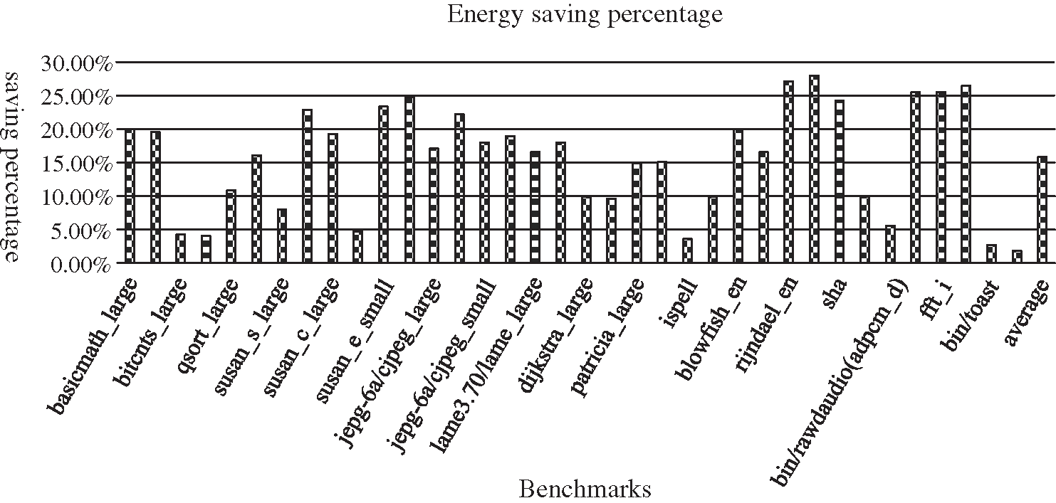
Figure 9: The space cost of DF reduction results for GMS
The experiment results demonstrate that our new register allocation method effectively increases the average raw dependent distance by making a lot of optimized, speculative executions allowing correct results, and greatly reduces the energy consumption wasted by speculation errors. Therefore, we have a very good auxiliary solution for TS architecture processors, especially for applications attempting a low energy consumption.
TS architecture is a promising trend for microprocessor development to improve the energy efficiency. Reducing the read-write dependencies can reduce timing error which in turn make more voltage down-scaling for TS processors. Optimized voltage scaling is beneficial for reducing the energy of processors. In this paper, we provide a DIGRR method to reduce the dependency of read-write between registers, with the objective of improving the energy efficiency of TS processors. The experiment results show that, more than 20% read-write dependency can be reduced on average, and the execution error rate is also reduced. As a result, energy consumption can be reduced by using lower voltage for TS processors.
Funding Statement:This work was supported by the General Project of Humanities and Social Sciences Research of the Ministry of Education(16YJA740039,Sheng Xiao, 2016); the Foundation Project of Philosophy and Social Science of Hunan (17YBA115,Sheng Xiao, 2018).
Conflicts of Interest:The authors declare that they have no conflicts of interest to report regarding the present study.
1. N. Chen, N. Xialihaer, W. Kong and J. Ren, “Research on prediction methods of energy consumption data,” Journal of New Media, vol. 2, no. 3, pp. 99–109, 2020. [Google Scholar]
2. N. R. Sivakumar, S. Ghorashi, M. Jamjoom and M. Alduaili, “Heuristic and bent key exchange secured energy efficient data transaction for traffic offloading in mobile cloud,” Computers Materials & Continua, vol. 65, no. 3, pp. 1925–1943, 2020. [Google Scholar]
3. Q. Liu, Z. Yang, X. Liu and S. Mbonihankuye, “Analysis of the efficiency-energy with regression and classification in household using k-nn,” Journal of New Media, vol. 1, no. 2, pp. 101–113, 2019. [Google Scholar]
4. S. Tabatabaei, “A novel fault tolerance energy-aware clustering method via social spider optimization (sso) and fuzzy logic and mobile sink in wireless sensor networks (wsns),” Computer Systems Science and Engineering, vol. 35, no. 6, pp. 477–494, 2020. [Google Scholar]
5. D. J. Ernst, N. S. Kim, S. Das, S. Pant, R. R. Rao et al., “A low-power pipeline based on circuit-level timing speculation,” in Proc.IEEE/ACM, Washington, DC, USA, pp. 7–18, 2003. [Google Scholar]
6. B. Greskamp and J. Torrellas, “Paceline: Improving single-thread performance in nanoscale cmps through core overclocking,” in Proc.PACT, Brasov, Romainia, pp. 213–224, 2007. [Google Scholar]
7. S. Xiao, J. He, X. Yang, Y. Wang and J. Lu, “Crosstalk aware register reallocation method for green compilation,” Computers, Materials & Continua, vol. 63, no. 3, pp. 1357–1371, 2020. [Google Scholar]
8. G. Hoang, R. Findler and R. Joseph, “Exploring circuit timing-aware language and compilation,” in Proc. ASPLOS, Newport Beach, CA, USA, pp. 345–356, 2011. [Google Scholar]
9. J. Sartori and R. Kumar, “Compiling for energy efficiency on timing speculative processors,” in Proc. DAC, San Francisco, CA, USA, pp. 1297–1304, 2012. [Google Scholar]
10. J. Xin and R. Joseph, “Identifying and predicting timing-critical instructions to boost timing speculation,” in Proc.DAC, Porto Alegre, RGS, Brazil, pp. 128–139, 2011. [Google Scholar]
11. B. Greskamp, L. Wan, U. R. Karpuzcu, J. J. Cook, J. Torrellas et al., “Designing processors for timing speculation from the ground up,” in Proc. IEEE/HPCA, Raleign,NC, USA, pp. 213–224, 2009. [Google Scholar]
12. A. B. Kahng, S. Kang, R. Kumar and J. Sartori, “Designing a processor from the ground up to allow voltage/reliability tradeoffs,” in Proc. IEEE/HPCA, Bangalore, Karnataka, India, pp. 213–224, 2010. [Google Scholar]
13. M. D. Powell, A. Biswas, S. Gupta and S. S. Mukherjee, “Architectural core salvaging in a multi-core processor for hard-error tolerance,” in Proc. SBAC/PAD, Sao Paolo, SP, Brazil, pp. 93–104, 2009. [Google Scholar]
14. X. Jiao, A. Rahimi, Y. Jiang, J. G. Wang, G. P. Gyvez et al., “CLIM: A cross-level workload-aware timing error prediction model for functional units,” IEEE Transactions on Computers, vol. 67, pp. 771–783, 2018. [Google Scholar]
15. L. Rioux, R. Henia and N. Sordon, “Using Model-Checking for Timing Verification in Industrial System Design,” in Proc. ICSTW, Tokyo, Tokyo, Japan, pp. 377–378, 2017. [Google Scholar]
16. H. Khdr, H. Amrouch and J. Henkel, “Dynamic guardband selection: Thermal-aware optimization for unreliable multi-core systems,” IEEE Transactions on Computers, vol. 68, pp. 53–66, 2019. [Google Scholar]
17. Y. Wang, J. C. Deng, Y. T. Fang, H. W. Li and X. W. Li, “Resilience-aware frequency tuning for neural-network-based approximate computing chips,” IEEE Transactions on Very Large Scale Integration Systems, vol. 25, pp. 2736–2748, 2017. [Google Scholar]
18. A. Meixner and D. J. Sorin, “Detouring: Translating software to circumvent hard faults in simple cores,” in Proc. ICSTW, Anchorage, AK, USA, pp. 80–89, 2008. [Google Scholar]
19. V. Reddi, S. Campanoni, M. S. Gupta, M. D. Smith, G. Wei et al., “Eliminating voltage emergencies via software-guided code transformations,” ACM Transactions on Architecture and Code Optimization, vol. 7, no. 12, pp. 1–28, 2010. [Google Scholar]
20. S. K. S. Hari, M. L. Li, P. Ramachandran, B. Choi and S. V. Adve, “Mswat: Low-cost hardware fault detection and diagnosis for multicore systems,” in Proc.IEEE/ACM, New York, NY, USA, pp. 122–132, 2009. [Google Scholar]
21. M. R. Guthaus, J. Ringenberg, D. J. Ernst, T. Austin, T. Mudge et al., “Mibench: A free, commercially representative embedded benchmark suite,” in Proc. IEEE/WWC, Washington, DC, USA, pp. 3–14, 2001. [Google Scholar]
22. C. Lee, M. Potkonjak and W. M. Smith, “MediaBench: A tool for evaluating and synthesizing multimedia and communications systems,” in Proc. IEEE/ACM, Saint Louis, MO, USA, pp. 330–335, 1997. [Google Scholar]
23. Y. F. Wu and J. R. Larus, “Static branch frequency and program profile analysis,” in Proc. IEEE/WWC, San Jose, CA, USA, pp. 1–11, 1994. [Google Scholar]
24. J. Sartori and R. Kumar, “Exploiting timing error resilience in processor architecture,” ACM Transactions on Embedded Computing Systems, vol. 2, no. 2s, pp. 46–57, 2013. [Google Scholar]
 | This work is licensed under a Creative Commons Attribution 4.0 International License, which permits unrestricted use, distribution, and reproduction in any medium, provided the original work is properly cited. |