DOI:10.32604/csse.2021.015544
| Computer Systems Science & Engineering DOI:10.32604/csse.2021.015544 | |
| Article |
Optimization of Bio-Implantable Power Transmission Efficiency Based on Input Impedance
1University of Technology, Department of Electrical Engineering, Baghdad, Iraq
2Almansour University College, Communication Engineering Department, Baghdad, Iraq
*Corresponding Author: Jaber H. Majeed. Email: 30085@Uotechnology.edu.iq
Received: 27 November 2020; Accepted: 23 January 2021
Abstract: Recently, the inductive coupling link is the most robust method for powering implanted biomedical devices, such as micro-system stimulators, cochlear implants, and retinal implants. This research provides a novel theoretical and mathematical analysis to optimize the inductive coupling link efficiency driven by efficient proposed class-E power amplifiers using high and optimum input impedance. The design of the coupling link is based on two pairs of aligned, single-layer, planar spiral circular coils with a proposed geometric dimension, operating at a resonant frequency of 13.56 MHz. Both transmitter and receiver coils are small in size. Implanted device resistance varies from 200 Ω to 500 Ω with 50 Ω of stepes. When the conventional load resistance of power amplifiers is 50 Ω, the efficiency is 45%; when the optimum resonant load is 41.89 Ω with a coupling coefficient of 0.087, the efficiency increases to 49%. The efficiency optimization is reached by calculating the matching network for the external LC tank of the transmitter coil. The proposed design may be suitable for active implantable devices.
Keywords: Inductive coupling link; power amplifier; matching network; implantable biomedical devices
Most bio-implantable devices, such as cochlear and retinal implants and micro-system stimulators, are powered using wires that breach the skin, causing patient discomfort and skin infections. Over the last few decades, implanted batteries have been used to power these devices, but due to the side effects of battery chemicals, limitations in size and lifetime, and the fact that changing batteries can be problematic, costly, or even hazardous for the patient [1], researchers have sought safer techniques to power these implantable devices.
The inductive coupling link method is now the common way to transfer both power and data to bio-implantable devices. There are four possible resonance inductive coupling topologies for connections in a passive system: serial to parallel (SP), parallel to serial (PS), serial-to-serial (SS), and parallel-to-parallel (PP). The most suitable connection for biomedical applications is the serial to parallel topology [2], where the primary circuit is tuned in series resonance to offer a low-impedance load for driving the transmitter coil, whereas the secondary coil (implanted coil) is almost invariably in parallel [3]. One of the main specifications for evaluating the performance of an inductive link [4,5] is Power Transfer Efficiency (PTE).
To acquire more than 70% of Power Transmission Efficiency (PTE), researchers consider only the self-impedance for a coupling link [1], which is usually several ohms. In fact, this is not an optimum way to calculate efficiency when the external coil is driven by a power amplifier. The power amplifier and source resistance must be added to the coupling link it self-impedance causing reducing the PTE by approximately 50% of its efficiency when the power amplifier resistance not consider. Most researchers consider the RF load resistance of a power amplifier as a conventional resistance, 50 Ω or 75 Ω, which presents the input impedance of the coupling link [6–8]. PTE can be optimized by calculating the optimum power amplifier load resistance and replacing it with the conventional resistance. In this paper, PTE optimization is achieved by determining the optimum inductive input impedance through calculating the matching network of the external LC tank and proposed a new geometric coil design by using the electromagnetic field solver HFSS 12.1 stimulator.
2 Optimum Resistance for Class-E Power Amplifiers at 13.56 MHz
The design of the power amplifier plays a significant role in low- and high-frequency bands by amplifying the input signal to a certain power level in order to drive the transmit circuit. One of the key factors in the design of the Power Amplifier (PA) is power efficiency. Eventually, the power efficiency of class-E and F power amplifiers have a better output efficiency compared to conventional amplifiers, such as classes A, B, C, and D [9]. The class-E amplifier is most commonly used in bio-implantable devices and telemetry systems due to its simple architecture and the fact that it requires only one active device [10]. In addition, when used as a modulator, it eliminates the need for a mixer that consumes power [11].
The aim is to design efficient class-E amplifiers for transcutaneous wireless transmission applications, such as implanted micro-systems, with optimum load resistance. In this application, the transmitted power is limited due to tissue absorption where the power is less than 200 mW. Suppose that Pout is 150 mW, f0 is 13.56 MHz, VCC is 3.3 V (DC), RL (load resistor) is 50 Ω, and the transistor is switching with 50% of duty cycle. To get optimum power from a class-E amplifier, we have to find the optimum resistance, RL.opt, by using Eq. (1) [12].
where, RL.opt = 41.89 Ω
For optimum power delivery, the load impedance or source impedance should be adjusted, hence, RL should be converted from 50 Ω to 41.89 Ω by using the matching network as given in Fig. 1.
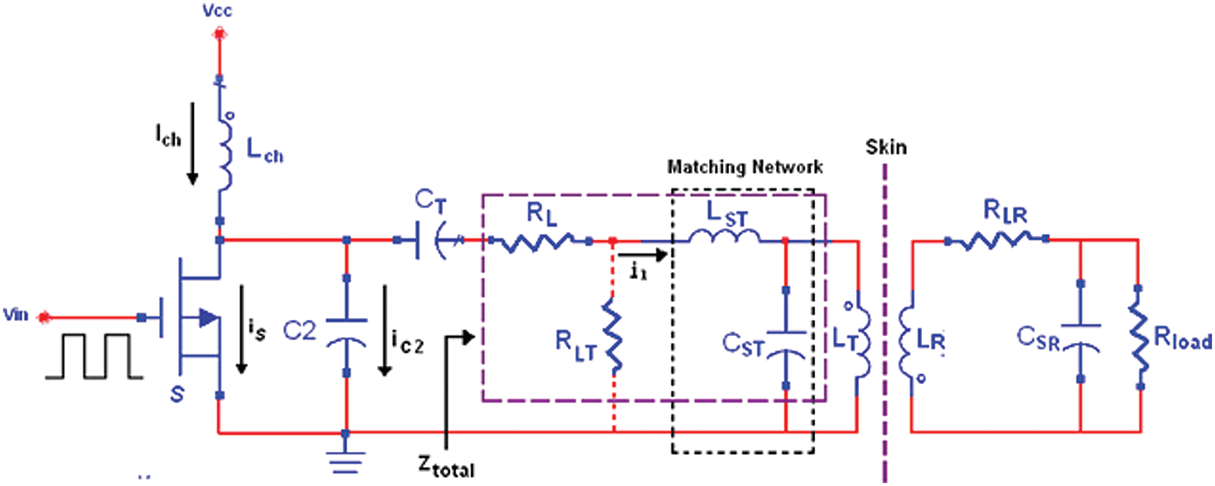
Figure 1: Inductive power transmission with matching network
The matching network-included capacitor (CST) and inductor (LST) are used to calculate parasitic resistance (resistor losses) for the transmitter coil.
The key to understanding the reduction of resistance is the equivalence between a series and parallel combination of a resistance (RL) and a reactance (±jX), as shown in Fig. 2.
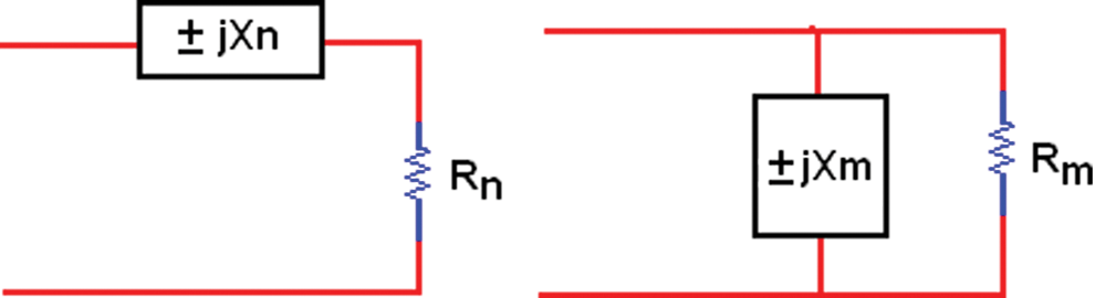
Figure 2: Conversions between series and parallel combinations
Considering Rn = 41.89 Ω and Rm = 50 Ω, then
The values of the matching network (CST) and inductor (LST) are found as follows:
(CST = 12.35 pf), (LST = 21.68 nH)
Hence, the parasitic resistance (RLT) can be calculated as given in
The total impedance of the matching network has a real part and imaginary part, as given in Fig. 2, and can be calculated as in the following (7) [13]:
where the real part impedance at operating frequency 13.56 MHz is approximately 41.89 Ω, and the imaginary part is approximately equal to zero (0.004311). The performance of the matching circuit is simulated by MATLAB as shown in Fig. 3.
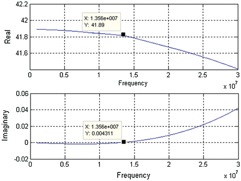
Figure 3: Real and imaginary impedance against frequency 13.56 MHz
4 Geometry of Coils and Transmission Distance Effect
In addition to optimum load resistance, there are two main factors that affect the design of coils Lt and Lr, which limits the overall efficiency of wireless power transmission system. The first factor is the ratio of the transmission distance (
The space employed by the implanted device limits the size of the receiver coil, which is placed within the human body and should be as small as possible. The transmitter coil is placed outside the body, so its size can be slightly larger to increase the distance of transmission. Power transmission efficiency decreases exponentially with distance and degrades significantly at far. For specified implanted coils, designing the size of a transmitter coil to increase the distance and power efficiency of the transmission is challenging.
The magnetic field strength (
If the coil size selection is not optimal, the strength of the magnetic field can be weak, resulting in a low PTE. The highest value of
where
This equation is approximate and does not consider the size and effect of the receiver coil. Therefore, there are optimal PSC geometries that would maximize efficiency.
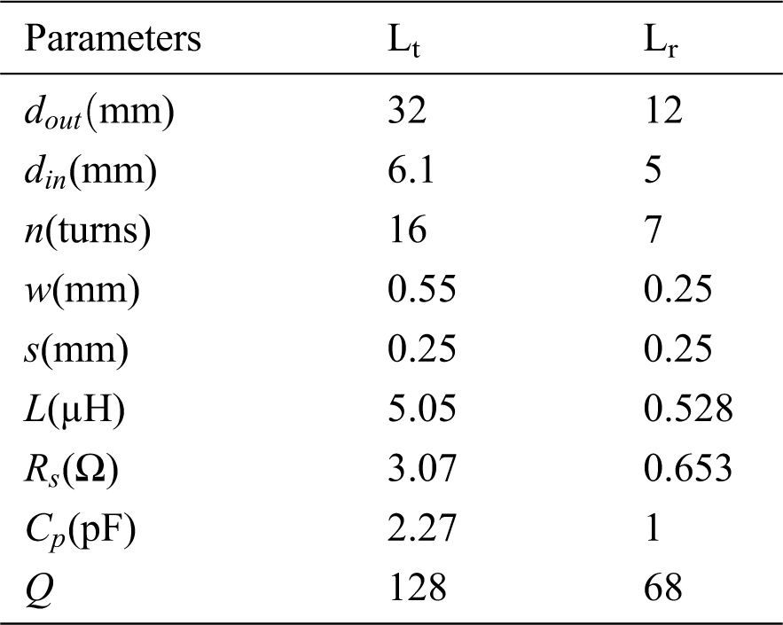
Fig. 4 and Tab. 1 show the geometric design of the transmitter and receiver coils, which should be carefully designed in terms of shape and geometry.
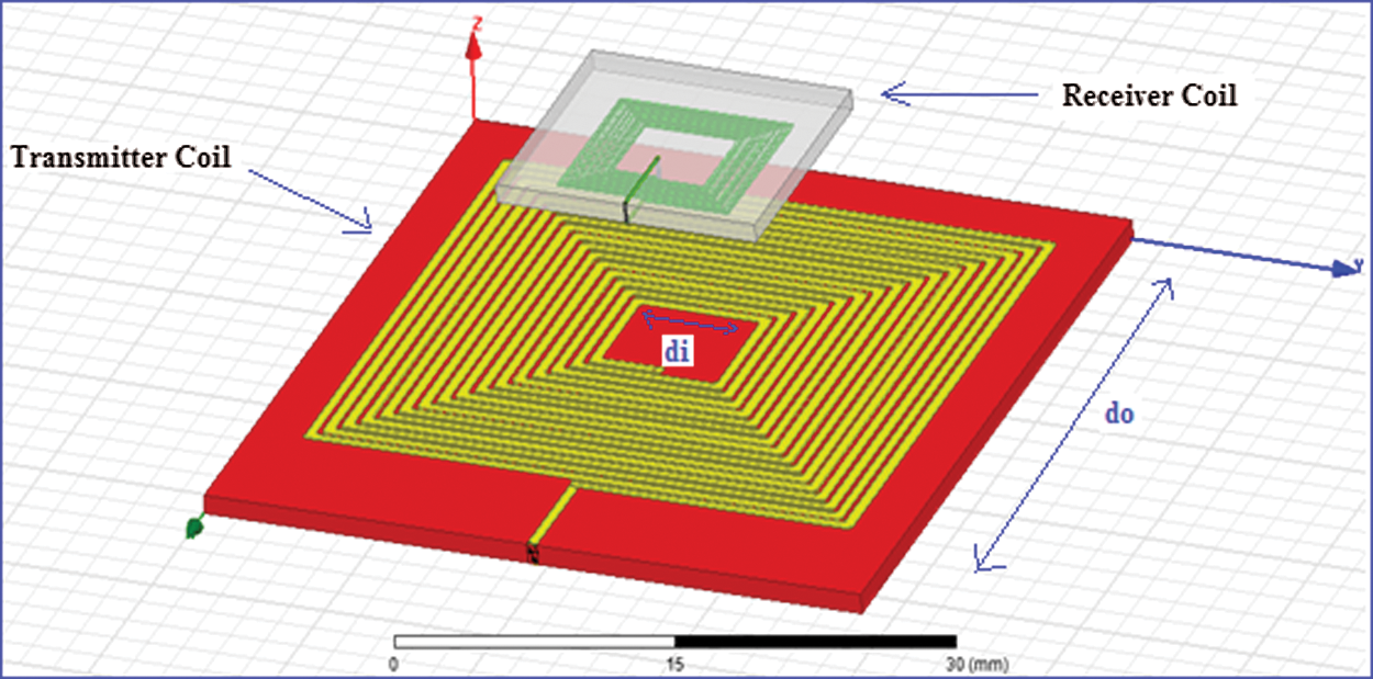
Figure 4: The transmitter and receiver coil model constructed HFSS 14.1 simulator
Table 1: Proposed and optimized geometries and inductive link parameters of the transmitter and receiver coils
5 Inductive Power Transmission and Simulation Results
The shape and size of the coupling coils have a significant impact on the efficiency of the system. In this research, the coil dimensions of the outer and inner transmitters are 32 mm and 6.1 mm, respectively, whereas implanted receiver coils are 12 mm and 5 mm, respectively [17]. The quality factor for the transmitter and receiver coils, Q1 and Q2, are calculated based on resonance frequency, parasitic resistance and coil inductance Eqs. (10), and (11):
where RLT and RLR represent the transmitter (reader) and receiver (implanted) coils’ parasitic resistance. The total power efficiency of the system has been calculated as follows:
The load resistance is Rload ≥ 2ωL2 [18], hence, it is assumed that Rload is between 200 Ω and 500 Ω, depending on implanted electronic remote resistance. Where in this work the reference Rload will be 500 Ω. Therefore, the power transmission efficiency using conventional input impedance (impedance of the coupling link) at 50 Ω is 45%. When an optimum load resistance of 41.89 Ω is used, the power transmission efficiency increases to 49%, as shown in Tab. 2 and Figs. 5a and 5b.
Table 2: Efficiency comparison between conventional and optimum input impedance
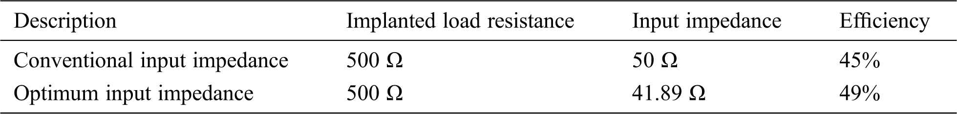
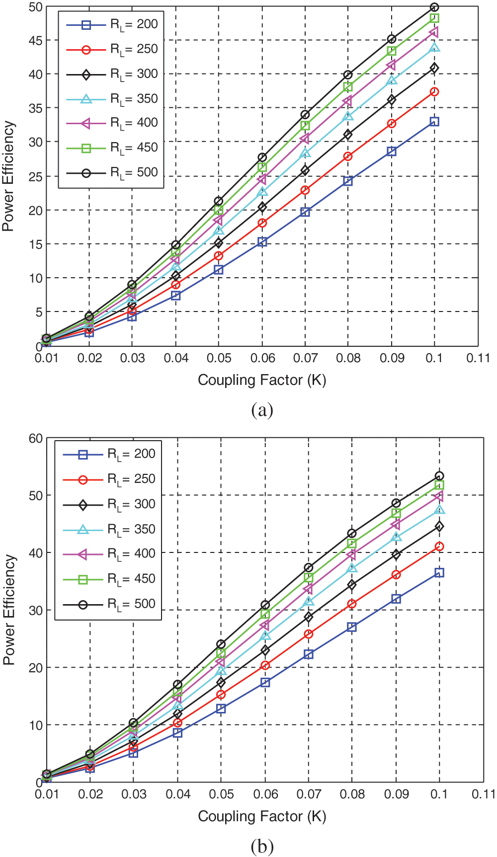
Figure 5: (a) PTE at input impedance 50 Ω (b) PTE at input impedance of 41.89 Ω
To verify these results, the proposed design is compared with other works, as shown in Tab. 3. The proposed design has greater efficiency even though the coil dimensions of other designers are larger than the proposed coil.
Table 3: Values of the proposed inductive compared with other works
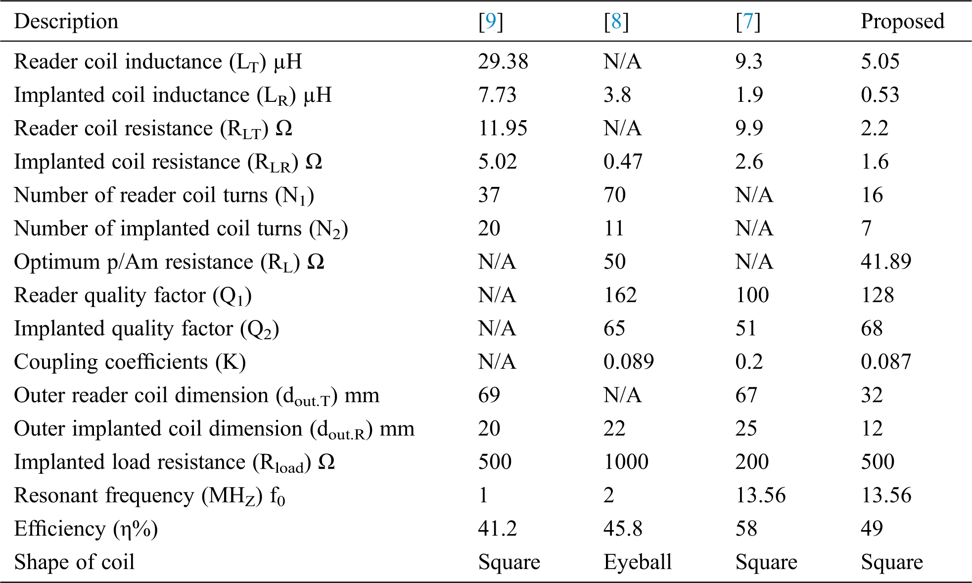
The inductive coupling link is widely used to power batteries in bio-implanted devices. Input impedance is the main factor effecting system efficiency. Most researchers used inductive self-impedance which is presented as parasitic resistance varied in several ohms. This is either not suitable, or they are assuming that the power amplifier resistance is 50 Ω as input impedance, which is suitable. In this paper, the optimum load resistance (Rload = 41.89 Ω) was used instead of 50 Ω by using a matching network. The total system efficiency increased from 45% to 49% with use of the optimal load instead of 50 Ω. These results are compared with other works as given in Tab. 1 where the performance of the proposed method is better.
Funding Statement: The authors received no specific funding for this study.
Conflicts of Interest: The authors declare that they have no conflicts of interest to report regarding the present study.
1. A. M. Hannan, S. Mutashar, A. S. Salina and A. Hussain. (2012). “Modulation techniques for biomedical implanted devices and their challenges,” Sensors, vol. 12, no. 1, pp. 297–319. [Google Scholar]
2. R. Jegadeesan and Y. X. Guo. (2010). “A study on the inductive power links for implantable biomedical devices,” in IEEE Antennas and Propagation Society Int. Sym., Toronto, Canada, pp. 11–17. [Google Scholar]
3. E. J. David, R. J. Johnny, L. H. John and D. S. Peter. (2006). “Basic electric circuit analysis,” Third edition, pp. 585–606. [Google Scholar]
4. C. Zierhofer and E. Hochmair. (1990). “High-efficiency coupling-insensitive transcutaneous power and data transmission via an inductive link,” IEEE Transactions on Biomedical Engineering, vol. 37, no. 7, pp. 716–722. [Google Scholar]
5. S. Atluri and M. Ghovanloo. (2005). “Design of a wideband power-efficient inductive wireless link for implantable biomedical devices using multiple carriers,” in Conf. Proc. 2nd Int. IEEE EMBS Conf. on Neural Engineering, New Jersey USA, pp. 533–537. [Google Scholar]
6. R. F. Xue, K. W. Cheng and J. Minkyu. (2013). “High efficiency wireless power transfer for biomedical implants by optimal resonant load transformation,” IEEE Transactions on Circuits and Systems 1: Regular Papers, vol. 60, no. 4, pp. 867–874. [Google Scholar]
7. K. Jungsuk, K. Hyunchul and D. P. Kenneth. (2011). “Power efficient inductive link optimization for implantable systems,” in IEEE Int. Conf. on radio and wireless symposium (RWSPhoenix, Arizona, USA, pp. 218–421. [Google Scholar]
8. U. M. Jow and M. Ghovanloo. (2007). “Design and optimization of printed spiral coils for efficient transcutaneous inductive power transmission,” IEEE Transection on Biomedical Circuits and Systems, vol. 1, no. 3, pp. 193–202. [Google Scholar]
9. X. HE. (2004). “Fully integrated transceiver design in SOI processes,” Kansas State University, Manhattan, Kansas, ProQuest Dissertations Publishing. [Google Scholar]
10. S. Mutashar, M. A. Hannan, S. A. Samad and A. Hussain. (2013). “Efficient low power recovery circuits for bio-implanted micro sensors,” Przegladelektrotechniczny (ERJ), vol. 89, no. 5, pp. 15–18. [Google Scholar]
11. M. K. Kazimierczuk. (1986). “Class E tuned power amplifier with nonsinusoidal output voltage,” IEEE Journal of Solid-State Circuits, vol. 21, no. 4, pp. 575–581. [Google Scholar]
12. L. H. Thomas. (2004). “The design of CMOS Radio frequency integrated circuits,” 2nd Edition Communications Engineer, vol. 2, no. 6, pp. 4–7. [Google Scholar]
13. A. Yahyai, I. Raisi, F. Sheryani, M. Hooti, F. Touati et al. (2009). , “High efficiency switching mode class-E power amplifier design for RF,” in IEEE Int. Conf. on Research and Development (SCOReD). Serdang Malaysia, pp. 1–4. [Google Scholar]
14. C. Yang, C. Chang, S. Lee, S. Chang and L. Chiou. (2017). “Efficient four coil wireless power transfer for deep brain stimulation,” IEEE Transactions on Microwave Theory and Techniques, vol. 65, no. 7, pp. 2496–2507. [Google Scholar]
15. K. Finkenzeller. (2010). RFID Handbook: Fundamentals and Applications in Contactless Smart Cards, Radio Frequency Identification and near-Field Communication, 3rd ed. John Wiley and Sons. [Google Scholar]
16. S. Mutashar, M. A. Hannan, S. A. Samad and A. Hussain. (2014). “Development of Bio-implanted micro-system with self recovery ASK demodulator for transcutaneous applications,” Journal of Mechanics in Medicine and Biology (JMMB), vol. 14, no. 04, pp. 1450062. [Google Scholar]
17. A. S. Ezzulddin and A. A. Ibraheem. (2017). “Design and optimization of printed spiral coils used in wireless power transmission systems for powering 10 mm2 receiver size at 13.56 MHz operating frequency,” Int. Journal of Current Engineering and Technology, vol. 7, no. 5, pp. 1835–1841. [Google Scholar]
18. S. Mutashar, M. A. Hannan, S. A. Samad and A. Hussain. (2012). “Efficient data and power transfer for bio-implanted devices based on ASK modulation techniques,” Journal of Mechanics in Medicine and Biology (JMMB), vol. 11, no. 5. [Google Scholar]
 | This work is licensed under a Creative Commons Attribution 4.0 International License, which permits unrestricted use, distribution, and reproduction in any medium, provided the original work is properly cited. |