
 Submit a Paper
 Propose a Special lssue
 Open Access
ARTICLE

Advancing PCB Quality Control: Harnessing YOLOv8 Deep Learning for Real-Time Fault Detection
1 Faculty of Cognitive Sciences and Human Development, Universiti Malaysia Sarawak, Kota Samarahan, 94300, Malaysia
2 School of Computer Science and Engineering, Anhui University of Science and Technology, Huainan, 232001, China
3 Department Electronic, Quaid-i-Azam University, Islamabad, 45320, Pakistan
* Corresponding Author: Fazal Shah. Email:
Computers, Materials & Continua 2024, 81(1), 345-367. https://doi.org/10.32604/cmc.2024.054439
Received 28 May 2024; Accepted 22 August 2024; Issue published 15 October 2024
 View Full Text
 Download PDF
Abstract
Printed Circuit Boards (PCBs) are materials used to connect components to one another to form a working circuit. PCBs play a crucial role in modern electronics by connecting various components. The trend of integrating more components onto PCBs is becoming increasingly common, which presents significant challenges for quality control processes. Given the potential impact that even minute defects can have on signal traces, the surface inspection of PCB remains pivotal in ensuring the overall system integrity. To address the limitations associated with manual inspection, this research endeavors to automate the inspection process using the YOLOv8 deep learning algorithm for real-time fault detection in PCBs. Specifically, we explore the effectiveness of two variants of the YOLOv8 architecture: YOLOv8 Small and YOLOv8 Nano. Through rigorous experimentation and evaluation of our dataset which was acquired from Peking University’s Human-Robot Interaction Lab, we aim to assess the suitability of these models for improving fault detection accuracy within the PCB manufacturing process. Our results reveal the remarkable capabilities of YOLOv8 Small models in accurately identifying and classifying PCB faults. The model achieved a precision of 98.7%, a recall of 99%, an accuracy of 98.6%, and an F1 score of 0.98. These findings highlight the potential of the YOLOv8 Small model to significantly improve the quality control processes in PCB manufacturing by providing a reliable and efficient solution for fault detection.Keywords
Smart technologies demand for more compact and powerful electronic devices that drive engineers to design PCBs with intricate layouts, enhancing functionality within limited space. However, this progress presents a challenge—PCBs become more susceptible to faults and defects [1]. Even minor imperfections in signal traces can disrupt electronic systems, necessitating rigorous quality control, particularly surface inspection [2]. Manual inspection methods, though labor-intensive and prone to errors, have traditionally been used for this purpose [3], especially with increasingly complex PCB designs.
As technology progresses and PCBs become more complex, the limitations of manual inspection become increasingly apparent [4]. No matter how skilled, the human eye is fallible, and its efficiency diminishes in the face of intricate designs, miniaturized components, and densely populated boards. The need for a more robust and efficient inspection system has led to a paradigm shift towards automation in the field of PCB quality control [5]. Early automated PCB inspection used high-resolution charge coupled device (CCD)/complementary metal oxide semiconductor (CMOS) sensors, representing a technological leap. However, accurately interpreting images was a challenge. Traditional machine vision struggled with precise pass/fail criteria, especially with limited failure samples. Advanced techniques were explored to overcome these challenges [6]. Convolutional Neural Networks (CNNs) have significantly improved image recognition and detection and can provide generalized solutions [7]. CNNs automatically learn image features without explicit extraction methods. AlexNet, a notable CNN, showed significant improvement in ImageNet LSVRC-2012, surpassing previous models by 10% [8]. CNNs have also demonstrated near-human performance in recognition tasks [9]. The objective of the research is to design and develop an effective PCB inspection system using YOLOv8. YOLOv8 is renowned for real-time processing and high accuracy in object detection. We evaluated YOLOv8-based models for fault detection in PCBs using an Open Lab dataset of 30,512 images [10]. Our assessment considered precision, recall, accuracy, mAP (Mean Average Precision), and IoU (Intersection over Union) thresholds to evaluate the model performance thoroughly. Traditional machine vision has limited accuracy and is not suited for the industrial context. Furthermore, manual inspection is very time-consuming, tedious, and prone to human errors. Therefore, we addressed the limitations of traditional machine vision and manual inspection using YOLOv8 for PCB inspection. The model was trained to recognize various faults, such as missing holes, open circuits, and incorrect placements. Our YOLOv8-based small Model effectively identified common defects in PCBs, as shown in Fig. 1 below.
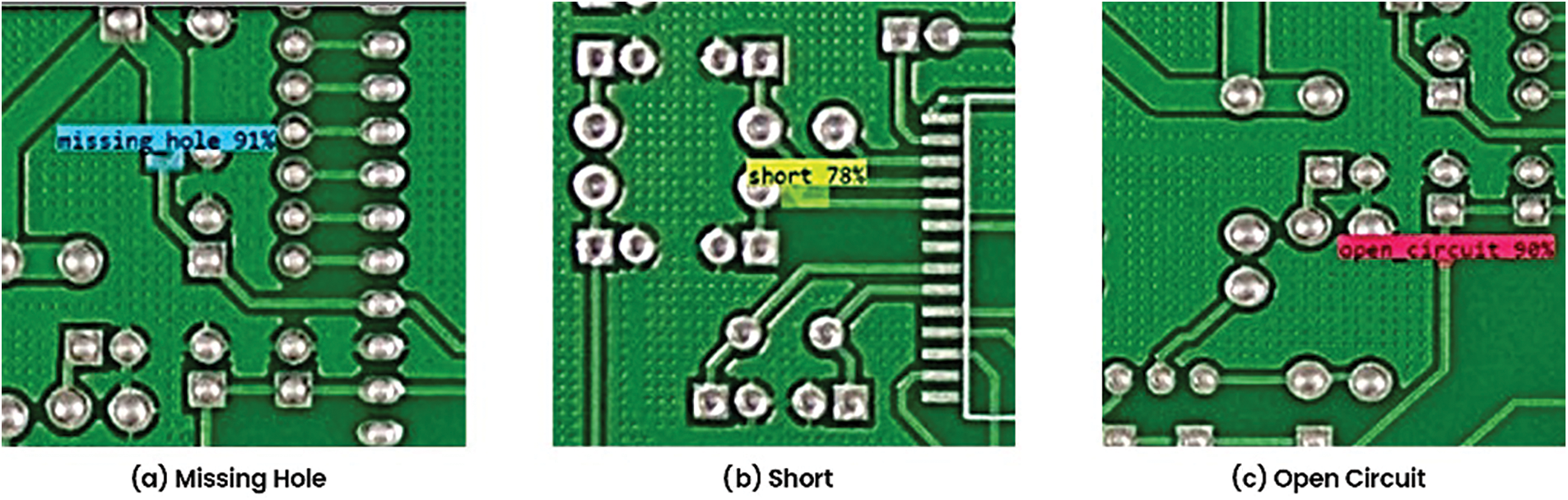
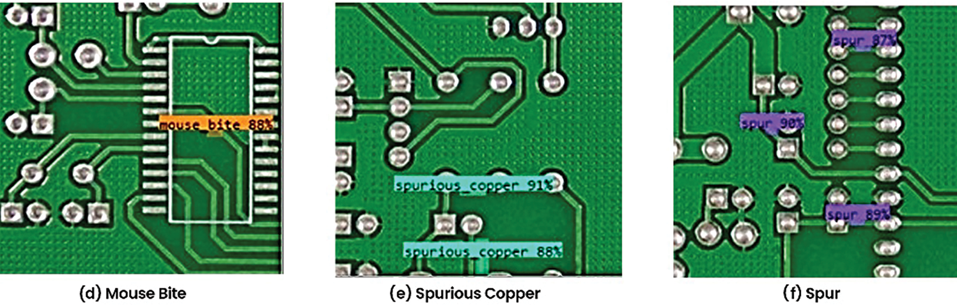
Figure 1: Detection by our YOLOv8-based models of common defects (a) Missing hole (b) Short (c) Open circuit (d) Mouse bite (e) Spurious copper (f) Spur
2.1 PCPs Defect Detection Using Machine Learning
For some time, conventional computer vision techniques have been utilized in PCB defect detection, combining image processing with classical machine learning algorithms [5]. Despite the rise of deep learning, traditional methods remain crucial, especially for interpretability, computational efficiency, and limited labelled data [11]. Deep learning models have revolutionized object detection, enabling automated identification, classification, and localization of defects [12,13]. These techniques leverage labelled data to learn patterns and relationships, significantly advancing PCB defect detection as evidenced by extensive literature [14,15]. Recent studies have extensively explored supervised learning, particularly Convolutional Neural Networks (CNNs), showcasing their effectiveness in learning hierarchical features from raw image data for accurate defect classification.
Supervised learning, using labelled datasets of defective and non-defective PCB images, is common in defect detection. CNNs are favored for automatically learning hierarchical features from raw image data [7]. Trained end-to-end on large datasets, CNNs extract relevant features and classify images into defect or non-defect categories [16]. Transfer learning techniques have been particularly effective in scenarios with limited labelled data [17]. Beyond CNNs, architectures like RNNs (Recurrent Neural Networks) and GANs (Generative Adversarial Networks) hold promise in PCB defect detection. RNNs, like LSTM (Long Short-Term Memory) networks, capture temporal dependencies in assembly images, while GANs generate synthetic defect images for data augmentation or unsupervised anomaly detection [11]. Shen et al. [18] explored LSTM networks for temporal dependencies in assembly images. Yu et al. used GANs to generate synthetic defect images and unsupervised anomaly detection [19].
Ensemble learning techniques, such as Random Forests and Gradient Boosting Machines (GBMs), were applied to improve classification accuracy and robustness in PCB defect detection. These methods combined multiple base classifiers to make predictions, which are particularly useful in scenarios with complex data distributions or imbalanced datasets. Ensemble learning techniques discussed by Li et al. [20] have been utilized to improve classification accuracy and robustness in PCB defect detection. Clustering algorithms group similar features, and autoencoders have been used for PCB defect detection. Auto encoders identify deviations from learned representations, signalling potential defects [21].
Furthermore, in [22], the researchers have explored the use of variational autoencoders (VAEs) to estimate reconstruction uncertainty and detect anomalies in PCB images, contributing to the field of unsupervised fault detection techniques. As studied by [23], semi-supervised learning methods used labelled and unlabelled data for PCB defect detection. Semi-supervised CNNs, initialized with pre-trained weights on unlabelled datasets and fine-tuned on labelled PCB images, improved performance and robustness in defect classification tasks.
YOLO, which stands for You Only Look Once, is a single-stage object detection network that contrasts with two-stage networks like R-CNN (Region-CNN) and Faster R-CNN [9,24]. While YOLO’s accuracy may be slightly lower, its detection speed is faster, maintaining excellent accuracy [25,26]. Many scholars have utilized YOLO networks to enhance object detection results [27]. The YOLO represents a paradigm shift in object detection networks, distinguished by its one-stage approach [28]. In contrast to R-CNN [7] and Faster R-CNN, the YOLO series is efficient in requiring only a single pass over the image to generate the detection results [29].
The YOLO object detection algorithm has evolved significantly from version 1 to version 8, improving accuracy, speed, and overall performance [30]. Fig. 2 visually depicts this evolution from YOLOv1 in 2015 to the latest iteration, YOLOv8, introduced in 2023.
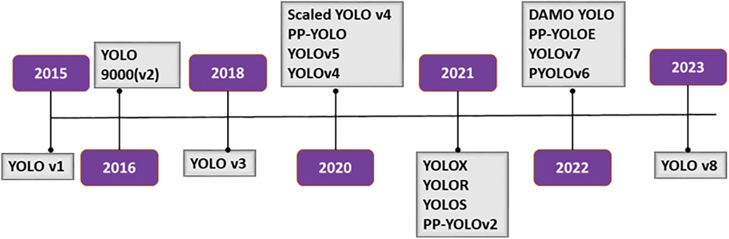
Figure 2: YOLO object detection methods timeline
The YOLOv8 architecture introduces changes like replacing the initial 6 × 6 convolution with a 3 × 3 convolution in the stem and incorporating Concatenated Bottleneck Stem (CBS) in C2f (Channel-to-Pixel) and C3 (Cross Stage Partial Bottleneck with 3 convolutions) [31]. Fig. 3 illustrates the YOLOv8 C2f Module’s design for efficient feature extraction and fusion. It begins with a Convolutional Block with Stride (CBS) operation, down-sampling spatial dimensions and extracting essential features. Subsequent concatenation operations fused feature maps from different network stages, enabling multi-scale information utilization for better object detection. A bottleneck structure within the module reduces computational complexity while maintaining representational capacity, enhancing feature extraction and fusion efficiency.
Figure 3: YOLOv8 C2f module
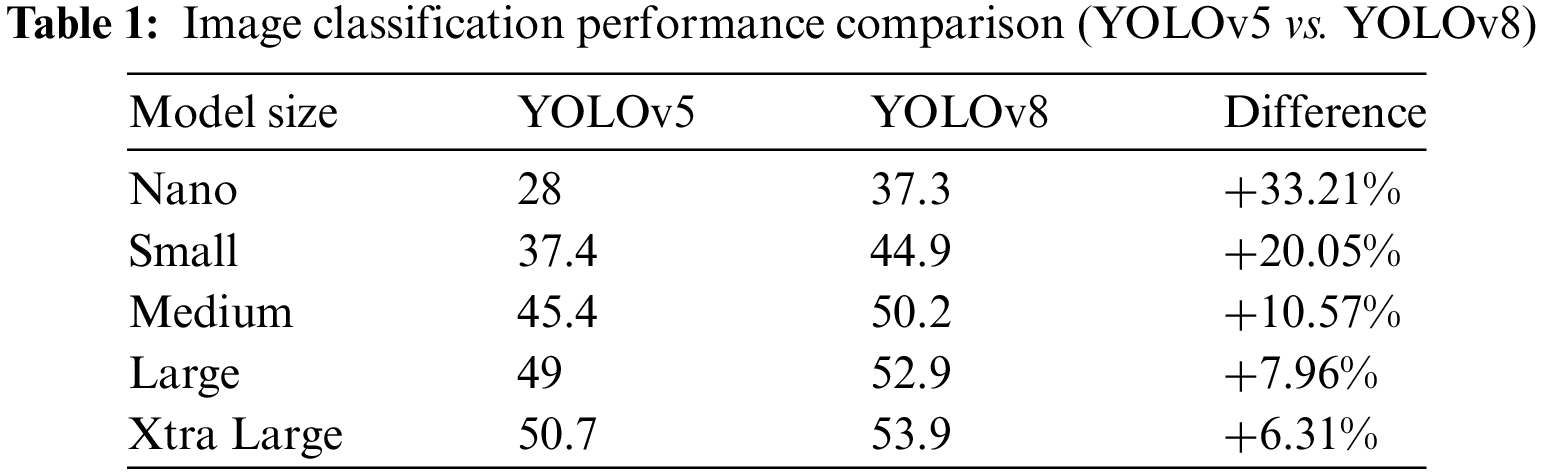
YOLOv8 utilizes mosaic augmentation, combining four images to diversify training scenarios for better object detection. The anchor-free model simplifies detection by predicting object centers, which is crucial for precise localization in PCBs. Table 1 compares classification performance between YOLOv5 and YOLOv8, highlighting differences in model size and capabilities.
Recently, domestic studies have applied YOLO-based detection. For example, Lan et al. [32] applied YOLOv3 in complex and multiple target backgrounds. Their model achieved high accuracy in real-time operations. The YOLO (You Only Look Once) model has been extensively used worldwide, and its performance and speed are increasing. Researchers like Bochkovskiy et al. [33] used YOLOv4 for real-time object detection in autonomous vehicles, achieving high accuracy and efficiency. Most of the local studies focused on agriculture, while international research seems to focus on various fields, such as autonomous vehicles and real-time processing. However, there is a gap in the integration of YOLO in PCB, and the aim of this study is to bridge the gap.
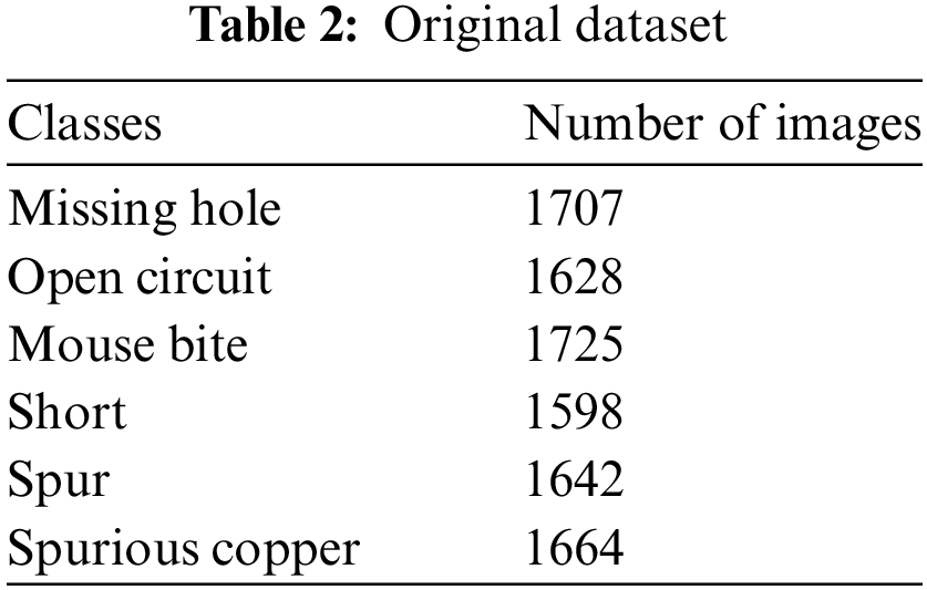
The PCB dataset used here originates from TDD (Test Driven Development)-net [34], a small fault detection network for PCBs provided by Peking University’s Open Lab on Human-Robot Interaction. It comprises 9964 images and annotations, showcasing various PCB configurations and simulated defects, including Missing Holes, Rate Bites, Open Circuit, Short, Spur, and Spurious Copper. These defects mimic common real-world PCB anomalies encountered during manufacturing and usage, as shown in Fig. 4 and Table 2 below.
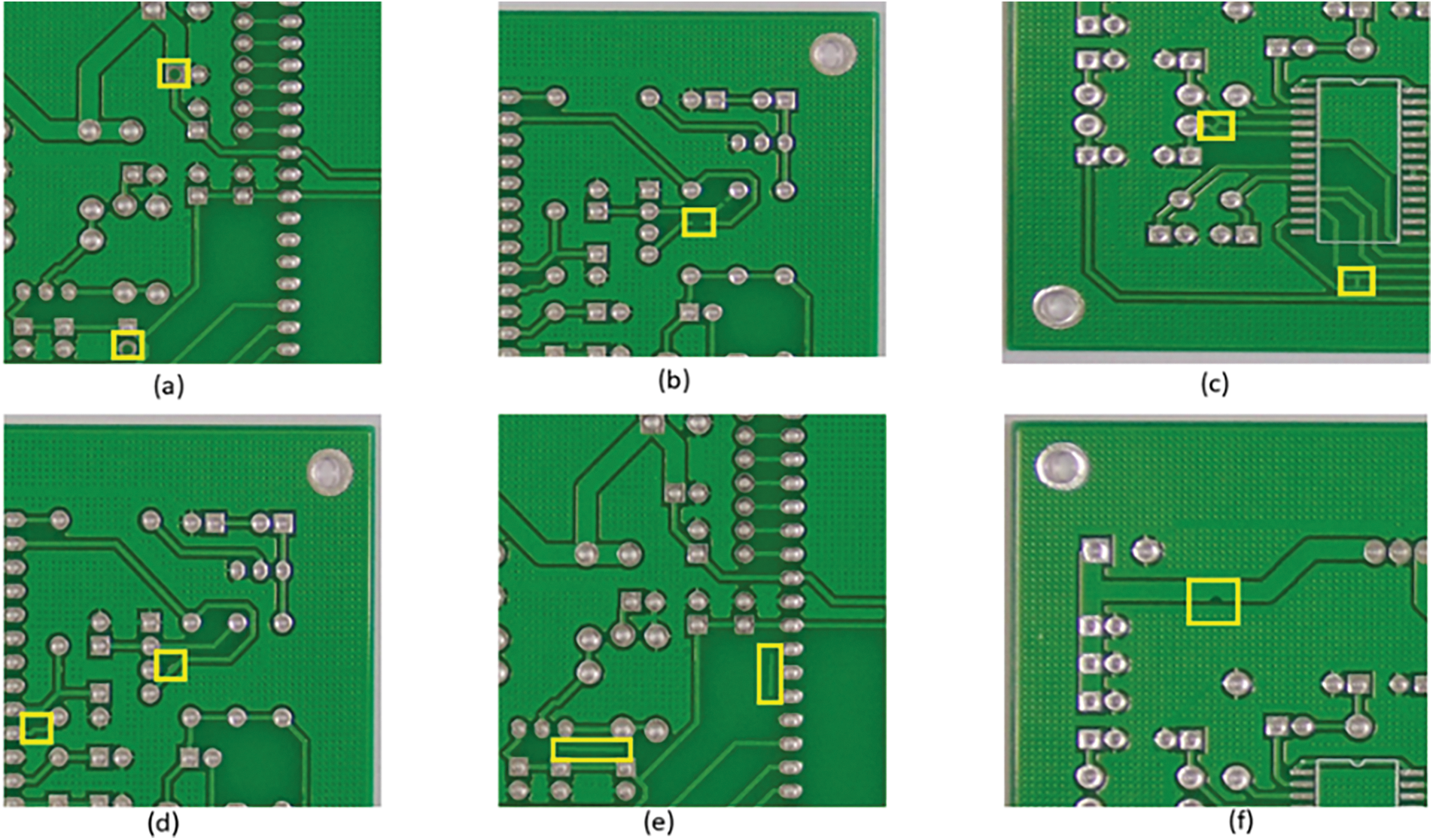
Figure 4: PCB defects (a) Missing hole (b) Open circuit (c) Short (d) Spur (e) Spurious copper (f) Mouse bite
The PCB dataset was annotated using Roboflow, where images were imported, and classes for components and fault types were defined, as shown in Fig. 5 below. Bounding box annotation tools were used to label regions of interest, with iterative refinement allowing for adjustments. Roboflow’s dataset management features aided organization and versioning.
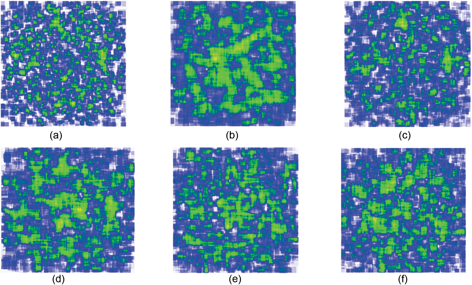
Figure 5: Annotation heatmap of all classes (a) Open circuit (b) Short (c) Mouse bite (d) Spur (e) Spurious copper (f) Missing hole
3.3 Pre-Processing and Augmentation
The dataset for our PCB fault detection model underwent thorough pre-processing and augmentation to optimize its suitability for training. Standardization of the average image size to 0.36 megapixels ensured uniform representation. Auto-orientation aligned images consistently and resized them to a 640 × 640 pixels standardized input size while introducing augmentation. Each training example yielded three outputs, diversifying the dataset and promoting a better understanding of PCB configurations and fault instances.
Horizontal and vertical flips were incorporated into the augmentation process, expanding the dataset by introducing mirrored versions of the original images. This horizontal and vertical mirroring helped the model generalize better than before by exposing it to component placement and orientation variations commonly encountered in real-world PCBs. Cropping, another augmentation technique, was applied with a minimal zoom of 0% and a maximum zoom of 20%. This feature introduced variability in the dataset by presenting different scales of the same images, mimicking varying distances or perspectives. Such variations are crucial for training a model that can effectively identify faults across scales and zoom levels.
Color representations were diversified through adjustments in saturation and exposure. Saturation levels were varied between −25% (desaturation) and +25% (enhanced saturation), introducing a range of color tones to the dataset. Similarly, exposure levels were modulated between −10% (reduced exposure) and +10% (increased exposure), contributing to variations in brightness. These adjustments simulated the diverse lighting conditions encountered in real-world scenarios, preparing the model for the challenges of detecting faults in varying environmental conditions.
To replicate real-world imperfections, up to 0.61% of pixels in each image underwent noise simulation. This introduced subtle irregularities, enhancing dataset realism and aiding the model in identifying faults amidst image noise. These pre-processing and augmentation measures greatly enhanced dataset diversity and robustness. Variations introduced through resizing, flipping, cropping, and color adjustments simulated real-world complexities, providing the fault detection model with a comprehensive training set. The deliberate noise introduction challenges the model to discern genuine faults from image irregularities.
This research utilised Google Colab’s computational power, specifically NVIDIA Tesla K80 GPUs, to expedite training deep learning models like YOLOv8. Leveraging GPUs (Graphics Processing Unit) accelerate complex model training by handling intensive tasks, reducing training times, and enhancing efficiency. Google Colab’s accessibility and scalability make it ideal for PCB defect detection research, where large dataset processing and model training are common. We employed Google Colab to train and evaluate YOLOv8 models on a dataset of 30,512 PCB images, facilitating accurate and efficient defect detection performance assessment.
In our experiment, we trained and fine-tuned both YOLOv8 Small and YOLOv8 Nano models on the same annotated PCB image dataset. We utilised transfer-learning techniques for defect detection tasks, to ensure that both models had access to the same data and underwent comparable training procedures. Fig. 6 illustrates the workflow.

Figure 6: Model workflow
YOLOv8 utilized a modified CSPDarknet53 as its backbone network to improve feature extraction and overall performance. This network underwent downsampling five times, generating five scale features labelled B1-B5. The structure is illustrated in Fig. 7 below.
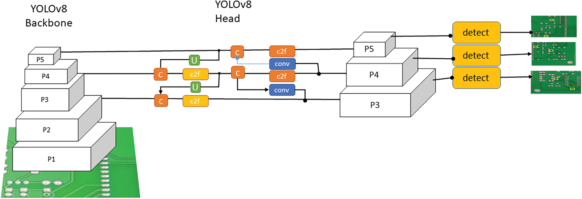
Figure 7: Model architecture
YOLOv8 substituted the Cross Stage Partial (CSP) module with the C2f module to optimize feature extraction while maintaining computational efficiency. It included gradient shunt connections to boost information flow, enhancing efficiency while maintaining a lightweight model. Additionally, the CBS module applied convolutional operations on input data and then used batch normalization and activation through the SiLU (Sigmoid Gated Linear Unit) function. The backbone network finished with the Spatial Pyramid Pooling Fast (SPPF) module, which pooled the input feature maps into a fixed-size map to produce an adaptive size output.
Drawing from PANet (Path Aggregation Network), YOLOv8 integrated a PAN-FPN (Path Aggregation Network with Feature Pyramid Network) structure into its design. Unlike previous models like YOLOv5 and YOLOv7, YOLOv8 simplified the PAN structure by eliminating the convolution operation after up-sampling, maintaining performance while achieving a lightweight model. In the YOLOv8 PAN structure, two feature scales were denoted as P4-P5 and N4-N5, corresponding to PAN and FPN structures, respectively. Traditional Feature Pyramid Networks (FPNs) adopt a top-down approach for conveying deep semantic information, which may lead to the loss of object localization details. To address this, PAN-FPN merged PAN with FPN, creating a network structure that integrates both top-down and bottom-up pathways. This integration improved the learning of location information by merging P4-N4 and P5-N5 features, thereby enhancing path development in a top-down approach. Consequently, PAN-FPN achieved comprehensive feature fusion, merging shallow positional with deep semantic information. By integrating both top-down and bottom-up pathways, PAN-FPN guaranteed the complementary nature of shallow positional and deep semantic information, enhancing the diversity and completeness of features. This fusion enhanced the model’s efficiency in object detection and localization problems.
The detection mechanism in YOLOv8 utilizes a decoupled head structure, as illustrated in Fig. 7. Unlike traditional models, this architecture uses two distinct branches specifically designed for object classification and bounding box regression tasks. Each branch applies unique loss functions suited to its requirements. The binary cross-entropy loss (BCE Loss) was used for object classification, while distribution focal loss (DFL) and Complete Intersection over Union (CIoU) were used for bounding box regression.
The decoupled head structure of YOLOv8 improved detection and sped up its convergence. Separating classification and regression tasks into distinct branches allowed the model to independently focus on learning and optimising each aspect. This task compartmentalisation enabled more targeted training, capturing intricate patterns and nuances associated with object classification and localisation more effectively. Additionally, YOLOv8 adopted an anchor-free detection approach, simplifying the training process by eliminating predefined anchor boxes. This process reduced computational complexity and improved efficiency.
Additionally, YOLOv8 leveraged the task-aligned assigner technique to assign samples dynamically during training. This approach enhanced detection accuracy and robustness by adapting samples with their respective tasks, ensuring the model received diverse and representative training data.
The pre-processed dataset was divided into training (80%), validation (20%), and testing (20%) sets to facilitate model training and evaluation. The validation set was used to validate the model and tune hyperparameters, while the testing set served as an independent benchmark for evaluating model performance. Transfer learning techniques were applied to fine-tune the selected YOLOv8 model on the training set, with adjustments made to hyperparameters as necessary. Model performance was evaluated on the validation set to avoid overfitting and ensure robustness. During the training phase, both models underwent a rigorous training regimen to optimize their performance for defect detection. Hyperparameters such as learning rate, batch size, and optimization algorithms were carefully tuned to ensure optimal convergence and generalization.
To ensure a comprehensive and objective comparison, we established evaluation criteria encompassing various aspects of model performance. Key metrics included precision, recall, mean Average Precision (mAP), computational requirements, and deployment feasibility. By considering multiple performance indicators, we aimed to gain a holistic understanding of each model’s capabilities and limitations. Recall is the ratio of true positive predictions to actual positives, as shown in Eq. (1). Precision is the ratio of true positive predictions to all positive predictions, as shown in Eq. (2).
True Positive (TP) is the count of accurately predicted positive cases, whereas False Positive (FP) represents the count of incorrectly predicted positive cases. True Negative (TN) refers to the number of correctly identified negative cases, and False Negative (FN) signifies the number of incorrectly identified negative cases.
In Eq. (3), the F-Measure (FM) is computed using precision, recall, and their harmonic mean. Precision (P) denotes the ratio of true positive cases to the total number of cases predicted as positive, whereas recall (R) indicates the ratio of true positive cases to the total number of actual positive cases.
The F-Measure (FM) integrates precision and recall into a single metric that balances both. It is computed using the formula provided in Eq. (3).
This metric enables a thorough evaluation of a classification model’s performance by taking into account its ability to accurately identify positive cases and to detect all positive cases within the dataset.
In the YOLOv8 algorithm, the localization loss is calculated using the Complete Intersection over Union (CIoU) metric using Eq. (4) below:
Here, α shows the trade-off, and v measures the consistency of the aspect ratio. These parameters, α and v, are defined in Eqs. (5) and (6).
LCIoU represents localization loss, α shows trade-off, and v measures the aspect ratio consistency. Here, wgt and hgt denote the width and height of the ground truth box, while w and h denote the width and height of the predicted box. The term c refers to the diagonals of the smallest enclosing rectangle for the actual and predicted boxes, respectively.
The loss function covers the overlap area, centroid distance, and aspect ratio in bounding box regression, but it primarily focuses on aspect ratio differences rather than confidence levels. This emphasis can impede effective similarity optimization and precise positioning. EIoU (Expected Intersection over Union) improves upon CIoU by separating the aspect ratio influence factor to independently compute the lengths and widths of the target and anchor boxes. EIoU consists of overlap loss, centre distance loss, and width-height loss components. While the overlap loss and centre distance loss follow CIoU principles, the width-height loss directly minimises differences in the widths and heights of the target and anchor boxes, speeding up convergence. By leveraging the actual length and width discrepancies between the predicted and labelled boxes, EIoU enhances the back-propagation process and improves the detection performance of small targets.
Evaluating the YOLOv8 Nano model for PCB defect detection offered valuable insights into its performance across various metrics, revealing its effectiveness for real-world applications in industrial quality control. With a precision (P) score of 0.95 and a recall (R) score of 0.919, the model demonstrated commendable accuracy in identifying defect instances, as depicted in Fig. 8 and the confusion matrix in Fig. 9. Moreover, the mean Average Precision (mAP) values of 0.956 for mAP50 and 0.429 for mAP50-95 showcase the model’s consistent detection performance across different Intersection over Union (IoU) thresholds. Furthermore, its consistent performance across different IoU thresholds enhances its reliability in detecting defects under varying conditions, ensuring comprehensive defect detection capabilities.

Figure 8: Training loss, precision, recall, and mean average precision results of the YOLOv8n model
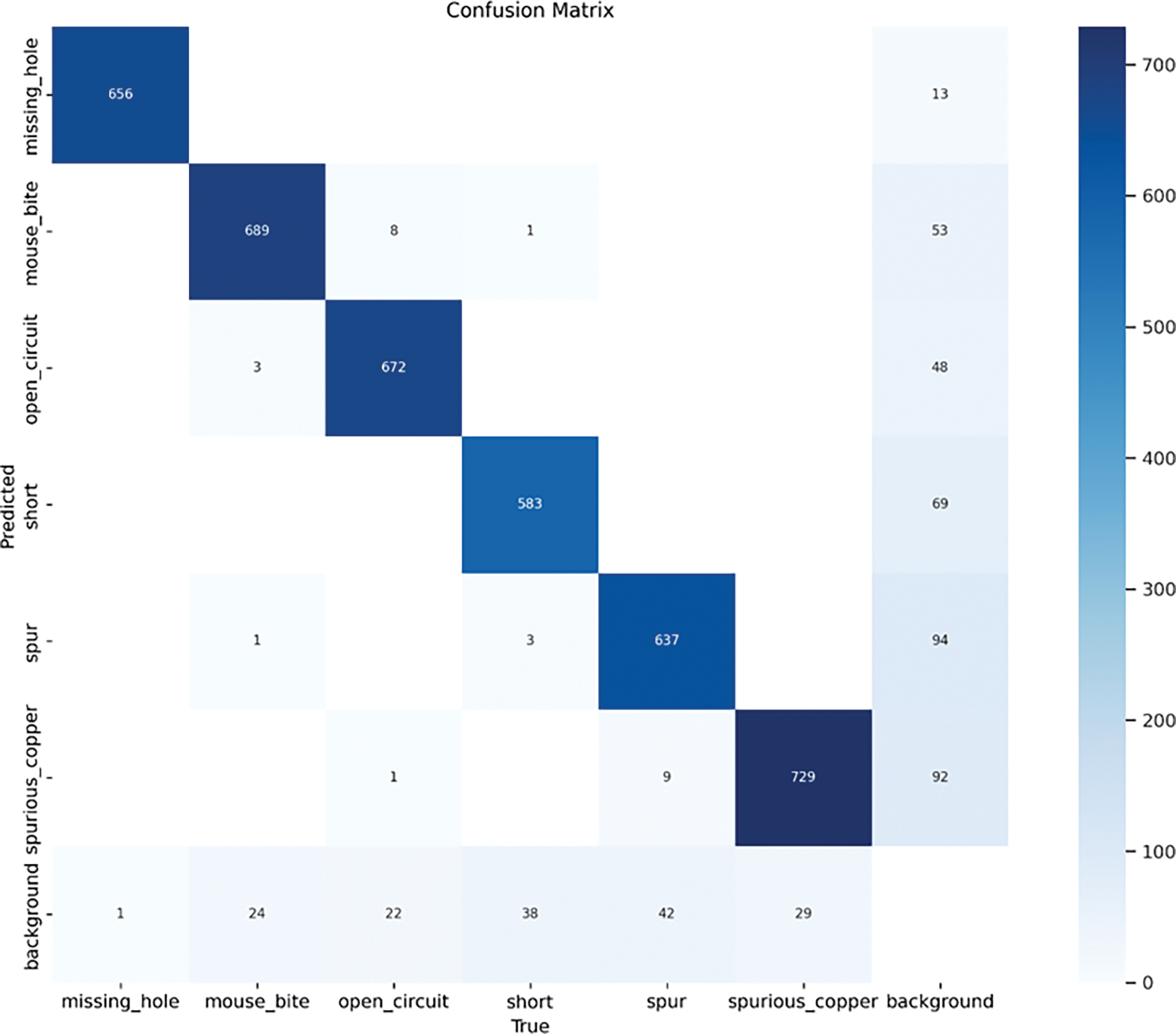
Figure 9: Confusion matrix of the YOLOv8n model
4.1.2 Model Precision Confidence in Fault Detection
The training results of the YOLOv8 Nano-based model revealed a remarkable confidence score of 1, attained at a confidence threshold of 0.89, as shown in Fig. 10. This exceptional precision level signified the model’s unparalleled accuracy at a relatively high confidence threshold, effectively minimizing false positive predictions.
Figure 10: Precision confidence curve of the YOLOv8n model
Its cautious labelling minimized false alarms, ensuring only genuine defects were flagged. This precision is due to the YOLOv8 Nano model’s advanced architecture and feature extraction, trained to discriminate accurately. The model’s conservative thresholding strategy prioritizes accuracy, reducing noise and false positives for reliable defect detection, which are crucial in industrial settings to prevent disruptions.
The F1 score is a comprehensive metric for assessing the model’s overall classification performance. A high F1 score signifies that the model effectively identifies defect instances while reducing both false positives and false negatives. Fig. 11 shows an F1 score of 0.93 at a confidence threshold of 0.370 across all classes. This indicated strong classification performance, effectively balancing precision and recall. The chosen confidence threshold represents the optimal operational point, maximizing the model’s F1 score and affirming its reliability in accurate classifications. Additionally, consistent F1 scores across all classes highlight the Nano model’s effective generalization capability, ensuring stable performance across diverse defect categories.
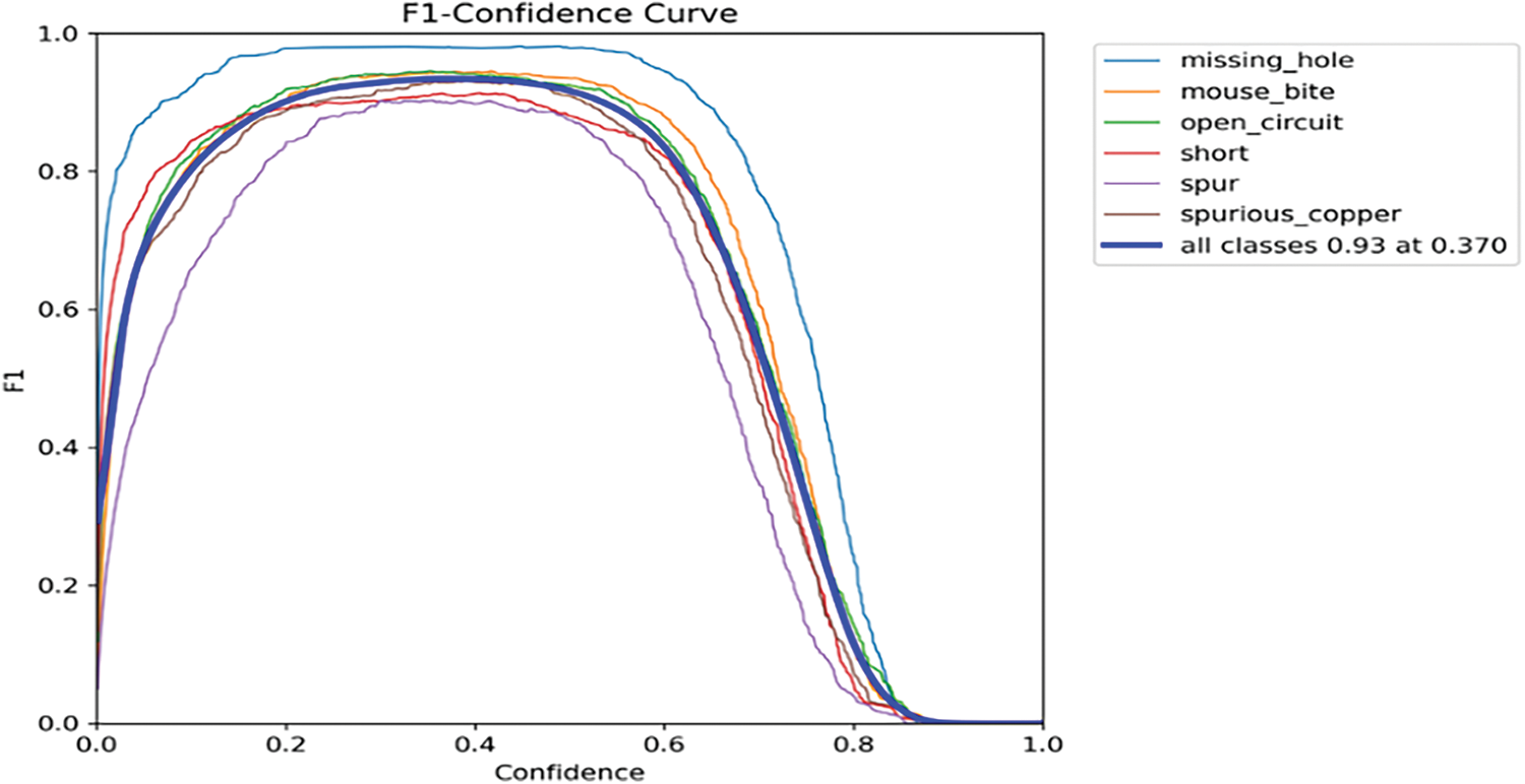
Figure 11: F1-Confidence curve
The model achieved a mean Average Precision (mAP) of 0.956 at an Intersection over Union (IoU) threshold of 0.5 for all classes, as depicted by the precision-recall curve in Fig. 12 below. The attainment of a high mAP score shows the model’s effectiveness in achieving both high precision and recall, which are vital for ensuring reliable defect detection systems. The mAP score of 0.956 demonstrates the model’s proficiency in accurately detecting defect instances across different categories in the PCB images. Precision performance is crucial for industries where even minor defects can lead to significant consequences in product performance and reliability. Industries can leverage this model to enhance quality control processes, ensuring the production of high-quality PCBs with minimal defects.
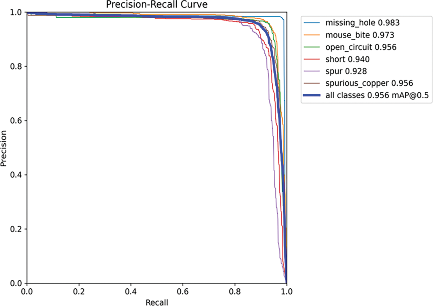
Figure 12: Precision recall curve of the YOLOv8n model
4.2 YOLOv8s Model Training Results
The evaluation of the YOLOv8 Small model for PCB defect detection shows its robust performance. The model effectively identifies defect instances with high precision and recall scores while minimising false positives and negatives. Additionally, the model shows outstanding mean Average Precision (mAP) values at various Intersections over Union (IoU) thresholds, highlighting its consistent detection performance and the dependable distinction between true positive and false positive detections.
In comparison to the YOLOv8 Nano model, the YOLOv8 Small model demonstrated superior detection accuracy and performance. Despite both models showing commendable precision and recall, the Small model outperformed the Nano model in mAP values, as depicted in Fig. 13. This indicated that the Small model excelled in capturing relevant defect instances, especially with varying degrees of overlap with ground truth annotations. Its effectiveness lies in its balanced architecture, achieving a harmonious balance between model complexity and detection accuracy. Unlike the Nano model prioritizing lightweight processing for resource-constrained environments, the small model offers enhanced detection capabilities without sacrificing computational efficiency. This makes it well-suited for applications requiring higher detection accuracy, such as industrial quality control in PCB manufacturing.
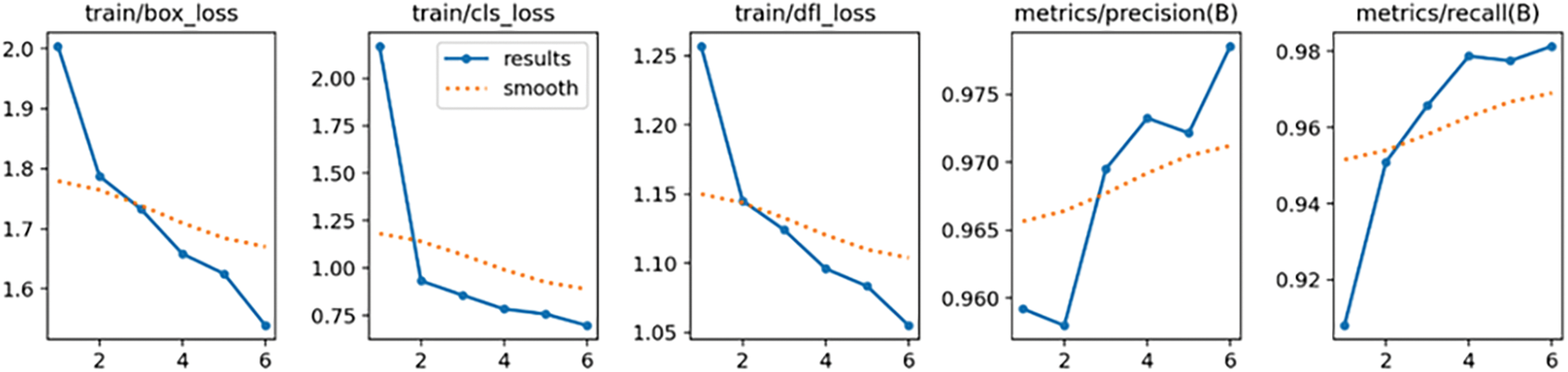
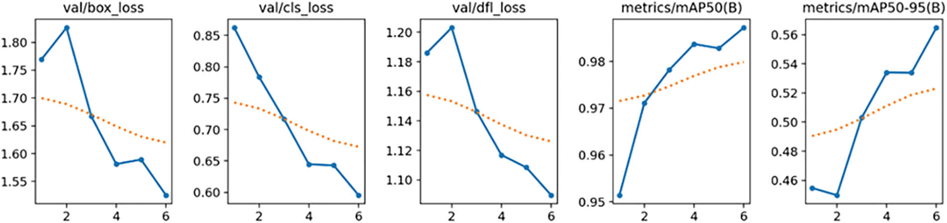
Figure 13: Training loss, precision, recall, and mean average precision results of the YOLOv8s model
Fig. 14 displays our model’s confusion matrix, contrasting predicted classifications with true ones across various classes like ‘missing hole’, ‘mouse bite’, ‘open circuit’, ‘short’, ‘spur’, ‘spurious copper’, and ‘background.’ Each cell in the matrix represents the prediction count for a specific pairing of predicted and true categories. The intensity of blue shading within cells indicates count magnitude, with darker shades indicating higher counts. Cells along the diagonal represent correct predictions (true positives), where the predicted category matches the true one, while off-diagonal cells represent errors (false positives and false negatives). Analyzing this matrix offers crucial insights into our model’s predictive capabilities and nuances.

Figure 14: Confusion matrix of the YOLOv8s model
Our model demonstrated excellent proficiency in accurately classifying specific defect categories. Particularly, ‘mouse bite,’ ‘open circuit,’ and ‘spurious copper’ showcase successful prediction, evident from the high true positive counts within corresponding diagonal cells of the matrix. This outstanding performance underscores the model’s ability to recognize subtle nuances and patterns within defect categories, ensuring highly accurate classification.
Furthermore, ‘missing hole’ emerges as another category wherein our model demonstrates notable success, evident from the substantial number of true positive counts encapsulated within the corresponding diagonal cells. However, amidst this triumph lies a tale of occasional misclassification, as evidenced by a small subset of instances wherein ‘missing hole’ is erroneously categorized as ‘background.’ This observation prompts a deeper inquiry into the underlying features and characteristics that may contribute to this misclassification, signalling a potential area for refinement and optimization within the model architecture.
Similarly, the ‘short’ category exhibits successes but challenges misclassifications, particularly with adjacent categories like ‘spur’ and ‘spurious copper.’ While the model accurately identifies ‘short’ defects, further exploration into distinguishing features is needed to improve discriminative capabilities. Similarly, the ‘spur’ category shows successes but complexities with misclassifications, highlighting the challenges in accurately classifying these defective categories.
The elements along the diagonal represent the samples accurately classified. Out of 4148 samples, 4090 were predicted correctly, resulting in an overall accuracy of 98.6%.
The findings indicated an F1 score of 0.98 with the YOLOv8 Small model using a confidence threshold of 0.408 for all classes, whereas the YOLOv8 Nano model attained an F1 score of 0.93 with a confidence threshold of 0.370 for all classes. These findings indicated that the YOLOv8 Small model surpassed the Nano model in terms of F1 score, reflecting a better balance between precision and recall.
The comparative analysis of F1 confidence curves highlighted the performance disparities between the YOLOv8 Small and YOLOv8 Nano models, as shown in Fig. 15 below. The higher F1 score attained by the Small model signified its superior precision and recall in defect detection tasks, indicating its potential for more accurate and reliable classifications. This suggested that the Small model may be better suited for applications where precision is critical, such as in quality control processes.

Figure 15: F1-Confidence curve of the YOLOv8s model
The results showed a precision-recall value of 0.987 mAP with the YOLOv8 Small model, using an IoU threshold of 0.5, while the YOLOv8 Nano model achieved a precision-recall value of 0.93 mAP at a comparable threshold, as shown in Fig. 16 below. These results indicated differences in the precision-recall characteristics between the two models, with the Small model demonstrating higher precision and recall values.
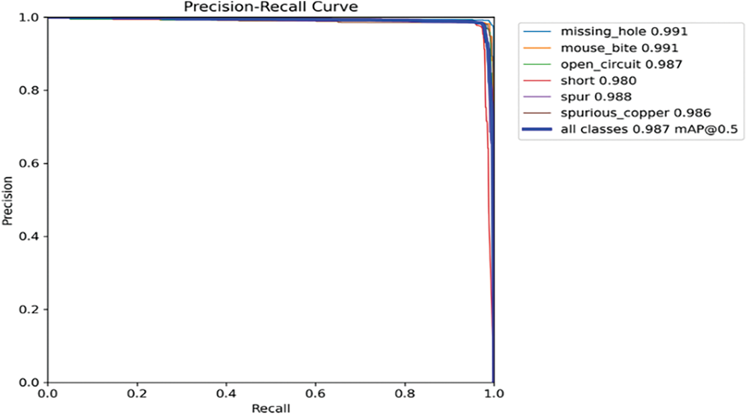
Figure 16: Precision recall curve of the YOLOv8s model
Moreover, the choice of IoU threshold plays a pivotal role in determining the precision-recall trade-off. A higher IoU threshold results in stricter criteria for accepting detected objects, leading to higher precision but potentially lower recall. Conversely, lowering the IoU threshold may improve recall at the expense of precision. Thus, understanding the implications of different IoU thresholds is crucial for optimising model performance according to specific application needs.
4.3 Performance Comparison with Other YOLO Versions
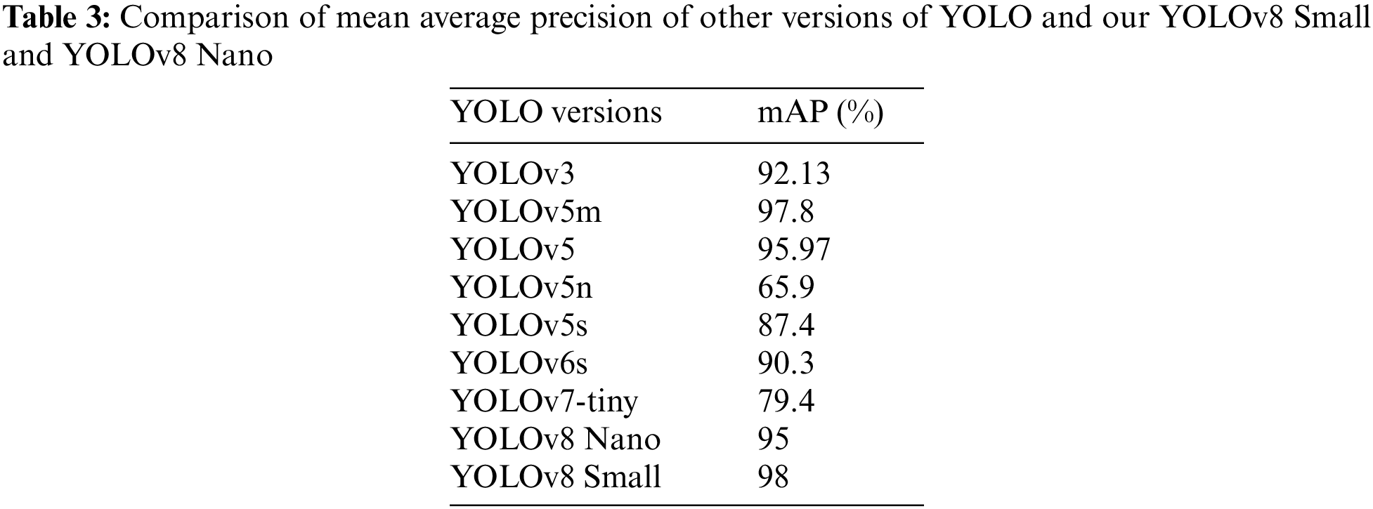
The YOLO-MBBi model [1] achieved a precision of 95.3% and a recall of 94.6% with a dataset size of 1200. Pan et al.’s YOLOv5m model achieved a precision of 97.8% [4]. Tang et al.’s YOLOv5 model achieved a precision of 95.97% [35]. Our proposed YOLOv8s model surpassed these with a precision of 98.7% and a recall of 99%. Furthermore, the YOLOv8 model handled a dataset size of 30,512 efficiently. These results underscored the YOLOv8 architecture’s effectiveness in achieving high precision and recall rates while managing larger datasets. Fig. 17 shows the fault detection in random images.

Figure 17: Detection of faults using random PCB images
The following Table 3 shows a comparison of YOLOv3 [32], YOLOv5m [4], YOLOv5 [35], and YOLOv7 [36] and our YOLOv8 Small and YOLOv8 Nano comparison.
While our study offers valuable insights into the efficacy of YOLOv8-based models for fault detection in printed circuit boards (PCBs), it is imperative to recognize the inherent limitations of our research. The narrow scope of our investigation, focusing solely on YOLOv8 Small and YOLOv8 Nano models, imposes constraints on the generalizability of our findings. This limitation underscores the necessity for broader exploration across a diverse array of deep learning architectures to understand their applicability in PCB fault detection comprehensively.
Moreover, it is crucial to diversify the datasets used for training and evaluation to enhance the robustness and applicability of research findings. While our study leveraged a specific dataset, extending research to encompass datasets with varying characteristics, such as size, complexity, and domain-specific challenges, will provide a more comprehensive assessment of model performance. By incorporating diverse datasets representative of real-world PCB inspection scenarios, researchers can better understand the generalizability of their findings and ensure the development of robust fault detection systems capable of handling a wide range of practical challenges.
This research demonstrated the efficacy of the YOLOv8 small-based deep learning model in enhancing fault detection in PCBs. Both YOLOv8 Small and YOLOv8 Nano achieved commendable levels of precision and recall, accurately identifying and classifying various fault types. Comparative analyses unveiled performance discrepancies between the two models, with YOLOv8 Small showcasing a marginally superior detection accuracy of 98.6%, necessitating more computational resources than YOLOv8 Nano, which has an accuracy of 95.6%. Our study findings underscored the robustness of YOLOv8 Small and YOLOv8 Nano models in defect detection within printed circuit boards, yielding a precision-recall value of 0.987 mAP at an IoU threshold of 0.5. In contrast, the latter achieved a slightly lower precision-recall value of 0.93 mAP at a comparable threshold, indicating a marginally decreased detection accuracy relative to YOLOv8 Small. This nuanced trade-off between detection accuracy and computational efficiency emphasizes the imperative of deliberating over factors such as model intricacy and resource demands when opting for a deep learning architecture for PCB fault detection tasks. Consequently, our findings underscored the critical significance of factoring in aspects like model complexity and computational efficiency while selecting a deep learning architecture tailored for PCB fault detection endeavors. Future research could explore optimizing the computational efficiency of the YOLOv8 models or developing hybrid approaches to balance accuracy and resource demands for enhanced PCB fault detection.
Acknowledgement: We gratefully acknowledge the support and resources provided by the School of Computer Science and Engineering, Anhui University of Science and Technology, Huainan, China, and the Research, Innovation and Enterprise Centre (RIEC) and Faculty of Cognitive Sciences and Human Development Universiti Malaysia Sarawak.
Funding Statement: This research did not receive any specific grant from funding agencies in the public, commercial, or not-for-profit sectors.
Author Contributions: The authors confirm their contribution to the paper as follows: study conception and design: Rehman Ullah Khan, Fazal Shah; data collection: Fazal Shah, Hamza Tahir, Ahmad Ali Khan; analysis and interpretation of results: Rehman Ullah Khan, Fazal Shah; draft manuscript preparation: Rehman Ullah Khan, Fazal Shah. All authors reviewed the results and approved the final version of the manuscript.
Availability of Data and Materials: The research data and related materials used are available at: https://github.com/Rehmanullah/PCB-Fault-Detection.git (accessed on 16 August 2024).
Ethics Approval: Not applicable.
Conflicts of Interest: The authors declare that they have no conflicts of interest to report regarding the present study.
References
1. B. W. Du, F. Wan, G. Lei, L. Xu, C. Xu and Y. Xiong, “YOLO-MBBi: PCB surface defect detection method based on enhanced YOLOv5,” Electronics, vol. 12, no. 13, 2023, Art. no. 2821. doi: 10.3390/electronics12132821. [Google Scholar] [CrossRef]
2. V. U. Sankar, G. Lakshmi, and Y. S. Sankar, “A review of various defects in PCB,” J. Electron. Test., vol. 38, no. 5, pp. 481–491, 2022. doi: 10.1007/s10836-022-06026-7. [Google Scholar] [CrossRef]
3. O. T. K. Thomas and P. P. Gopalan, “PCB defects,” in Electronics Production Defects and Analysis. Singapore: Springer, 2022, pp. 39–73. doi: 10.1007/978-981-16-9824-8. [Google Scholar] [CrossRef]
4. L. Pan et al., “Efficient and precise detection of surface defects on PCBs: A YOLO based approach,” in Proc. Adv. Intell. Comput. Technol. Appl., Zhengzhou, China, Springer, Aug. 10–13, 2023, vol. 14087, pp. 601–613. [Google Scholar]
5. Q. Ling and N. A. M. Isa, “TD-YOLO: A lightweight detection algorithm for tiny defects in high-resolution PCBs,” Adv. Theory Simul., vol. 7, no. 4, 2023, Art. no. 2300971. doi: 10.1002/adts.202300971. [Google Scholar] [CrossRef]
6. M. Yuan, Y. Zhou, X. Ren, H. Zhi, J. Zhang and H. Chen, “YOLO-HMC: An improved method for PCB surface defect detection,” IEEE Trans. Instrum. Meas., vol. 73, pp. 1–11, Apr. 2024, Art. no. 2001611. doi: 10.1109/TIM.2024.3351241. [Google Scholar] [CrossRef]
7. P. Wei, C. Liu, M. Liu, Y. Gao, and H. Liu, “CNN-based reference comparison method for classifying bare PCB defects,” J. Eng., vol. 2018, no. 16, pp. 1528–1533, Nov. 2018. doi: 10.1049/joe.2018.8271. [Google Scholar] [CrossRef]
8. A. Allah, H. Elahi, Z. Sun, A. Khatoon, and I. Ahmad, “Comparative analysis of AlexNet, ResNet18 and SqueezeNet with diverse modification and arduous implementation,” Arab. J. Sci. Eng., vol. 47, no. 2, pp. 2397–2417, Oct. 2021. doi: 10.1007/s13369-021-06182-6. [Google Scholar] [CrossRef]
9. F. Fan, B. Wang, G. Zhu, and J. Wu, “Efficient faster R-CNN: Used in PCB solder joint defects and components detection,” in IEEE 4th Int. Conf. Comput. Commun. Eng. Technol. (CCET), Beijing, China, 2021, pp. 1–5. doi: 10.1109/CCET52649.2021.9544356. [Google Scholar] [CrossRef]
10. Peking University Open Lab, “Printed circuit board (PCB) defect dataset,” Accessed: Aug. 09, 2024, 2022. [Online]. Available: https://robotics.pkusz.edu.cn/resources/datasetENG/ [Google Scholar]
11. A. Bhattacharya and S. G. Cloutier, “End-to-end deep learning framework for printed circuit board manufacturing defect classification,” Sci. Rep., vol. 12, no. 1, p. 12559, 2022. doi: 10.1038/s41598-022-16302-3. [Google Scholar] [PubMed] [CrossRef]
12. I. C. Chen, R. C. Hwang, and H. C. Huang, “PCB defect detection based on deep learning algorithm,” Processes, vol. 11, no. 3, p. 775, 2023. doi: 10.3390/pr11030775. [Google Scholar] [CrossRef]
13. V. -T. Nguyen and H. -A. Bui, “A real-time defect detection in printed circuit boards applying deep learning,” EUREKA: Phys. Eng., vol. 2, pp. 143–153, 2022. doi: 10.21303/2461-4262.2022.002127. [Google Scholar] [CrossRef]
14. J. -H. Park, Y. -S. Kim, H. Seo, and Y. -J. Cho, “Analysis of training deep learning models for PCB defect detection,” Sensors, vol. 23, no. 55, 2023, Art. no. 2766. doi: 10.3390/s23052766. [Google Scholar] [PubMed] [CrossRef]
15. V. A. Adibhatla, J. -S. Shieh, M. F. Abbod, H. -C. Chih, C. -C. Hsu and J. Cheng, “Detecting defects in PCB using deep learning via convolution neural networks,” in 13th Int. Microsyst. Packaging Assembl. Circuit. Technol. Conf. (IMPACT), Taipei, Taiwan, 2018. doi: 10.1109/IMPACT.2018.8625828. [Google Scholar] [CrossRef]
16. S. Mohapatra, A. Kabra, D. H. Gowda, S. S. Gaonkar, and S. Sadhukha, “PCB defect detection using CNN-based deep learning,” in Int. Conf. Soft Comput. Secur. Appl., Tamil Nadu, India, Springer, Apr. 17–18, 2023, vol. 1449, pp. 363–37. [Google Scholar]
17. L. K. Cheong, S. A. Suandi, and S. Rahman, “Defects and components recognition in printed circuit boards using convolutional neural network,” in 10th Int. Conf. Robot. Vis. Sig. Process. Pow. Appl.: Enabl. Res. Innovat. Towards Sustain., Singapore, Springer, Apr. 5–6, 2019, pp. 75–81. [Google Scholar]
18. J. Shen, N. Liu, and H. Sun, “Defect detection of printed circuit board based on lightweight deep convolution network,” IET Image Process., vol. 14, no. 15, pp. 3932–3940, 2020. doi: 10.1049/iet-ipr.2020.0841. [Google Scholar] [CrossRef]
19. X. Yu and Y. He, “PCB defect detection based on GAN data generation with self-attentive mechanism,” in 2nd Int. Conf. Front. Electron. Info. Comput. Technol. (ICFEICT), Wuhan, China, IEEE, 2022, pp. 55–60. doi: 10.1109/ICFEICT57213.2022.00018. [Google Scholar] [CrossRef]
20. Y. -T. Li, P. Kuo, and J. -I. Guo, “Automatic industry PCB board DIP process defect detection system based on deep ensemble self-adaption method,” IEEE Trans. Compon. Packaging Manufact. Technol., vol. 11, no. 2, pp. 312–323, 2020. doi: 10.1109/TCPMT.2020.3047089. [Google Scholar] [CrossRef]
21. R. A. Melnyk and R. B. Tushnytskyy, “Detection of defects in printed circuit boards by clustering the etalon and defected samples,” in IEEE 15th Int. Conf. Adv. Trends Radioelect. Telecommun. Comput. Eng. (TCSET), Lviv-Slavske, Ukraine, IEEE, 2020, pp. 961–964. doi: 10.1109/TCSET49122.2020.235580. [Google Scholar] [CrossRef]
22. S. Khalilian, Y. Hallaj, A. Balouchestani, H. Karshenas, and A. Mohammadi, “PCB defect detection using denoising convolutional autoencoders,” in Int. Conf. Mach. Vis. Image Process. (MVIP), Iran, IEEE, 2020, pp. 1–5. doi: 10.1109/MVIP49855.2020.9187485. [Google Scholar] [CrossRef]
23. Y. Wan, L. Gao, X. Li, and Y. Gao, “Semi-supervised defect detection method with data-expanding strategy for PCB quality inspection,” Sensors, vol. 22, no. 20, 2022, Art. no. 7971. doi: 10.3390/s22207971. [Google Scholar] [PubMed] [CrossRef]
24. W. Chen, Z. Huang, Q. Mu, and Y. Sun, “PCB defect detection method based on transformer-YOLO,” IEEE Access, vol. 10, pp. 129480–129489, 2022. doi: 10.1109/ACCESS.2022.3228206. [Google Scholar] [CrossRef]
25. X. Huo, “Development of a real-time Printed Circuit board (PCB) visual inspection system using You Only Look Once (YOLO) and fuzzy logic algorithms,” J. Intell. Fuzz. Syst., vol. 45, no. 3, pp. 4139–4145, 2023. doi: 10.3233/JIFS-223773. [Google Scholar] [CrossRef]
26. Y. -L. Lin, Y. -M. Chiang, and H. -C. Hsu, “Capacitor detection in PCB using YOLO algorithm,” in Int. Conf. Syst. Sci. Eng. (ICSSE), New Taipei, Taiwan, IEEE, 2018, pp. 1–4. doi: 10.1109/ICSSE.2018.8520170. [Google Scholar] [CrossRef]
27. K. Xia et al., “Global contextual attention augmented YOLO with ConvMixer prediction heads for PCB surface defect detection,” Sci. Rep., vol. 13, no. 1, p. 9805, 2023. doi: 10.1038/s41598-023-36854-2. [Google Scholar] [PubMed] [CrossRef]
28. X. Wang, H. Zhang, Q. Liu, W. Gong, S. Bai and H. You, “YOLO’s multiple-strategy PCB defect detection model,” IEEE Multimed., vol. 31, no. 1, pp. 76–87, 2024. doi: 10.1109/MMUL.2024.3359267. [Google Scholar] [CrossRef]
29. H. J. Yoon and J. J. Lee, “PCB component classification algorithm based on YOLO network for PCB inspection,” J. Korea Multimed. Soc., vol. 24, no. 8, pp. 988–999, 2021. [Google Scholar]
30. J. Li, J. Gu, Z. Huang, and J. Wen, “Application research of improved YOLO V3 algorithm in PCB electronic component detection,” Appl. Sci., vol. 99, no. 18, 2019, Art. no. 3750. doi: 10.3390/app9183750. [Google Scholar] [CrossRef]
31. J. Terven, D. -M. Córdova-Esparza, and J. -A. Romero-González, “A comprehensive review of YOLO architectures in computer vision: From YOLOv1 to YOLOv8 and YOLO-NAS,” Mach. Learn. Knowl. Extract., vol. 5, no. 4, pp. 1680–1716, 2023. doi: 10.3390/make5040083. [Google Scholar] [CrossRef]
32. Z. Lan, Y. Hong, and Y. Li, “An improved YOLOv3 method for PCB surface defect detection,” in Proc. IEEE Int. Conf. Pow. Electron., Comput. Appl. (ICPECA), Shenyang, China, 2021, pp. 1009–1015. doi: 10.1109/ICPECA51329.2021.9362675. [Google Scholar] [CrossRef]
33. A. Bochkovskiy, C. -Y. Wang, and H. -Y. M. Liao, “YOLOv4: Optimal speed and accuracy of object detection,” 2020, arXiv:2004.10934. [Google Scholar]
34. R. Ding, L. Dai, G. Li, and H. Liu, “TDD-net: A tiny defect detection network for printed circuit boards,” CAAI Trans. Intell. Technol., vol. 44, no. 2, pp. 110–116, 2019. doi: 10.1049/trit.2019.0019. [Google Scholar] [CrossRef]
35. J. Tang, S. Liu, D. Zhao, L. Tang, W. Zou and B. Zheng, “PCB-YOLO: An improved detection algorithm of PCB surface defects based on YOLOv5,” Sustainability, vol. 15, no. 7, 2023, Art. no. 5963. doi: 10.3390/su15075963. [Google Scholar] [CrossRef]
36. Y. Long, Z. Li, Y. Cai, R. Zhang, and K. Shen, “PCB defect detection algorithm based on improved YOLOv8,” Academ. J. Sci. Technol., vol. 7, no. 3, pp. 297–304, 2023. doi: 10.54097/ajst.v7i3.13420. [Google Scholar] [CrossRef]
Cite This Article
 Copyright © 2024 The Author(s). Published by Tech Science Press.
This work is licensed under a Creative Commons Attribution 4.0 International License , which permits unrestricted use, distribution, and reproduction in any medium, provided the original work is properly cited.
 Downloads
 Citation Tools