
 Submit a Paper
 Propose a Special lssue
 Open Access
ARTICLE

FPGA Accelerators for Computing Interatomic Potential-Based Molecular Dynamics Simulation for Gold Nanoparticles: Exploring Different Communication Protocols
1 Department of Electrical Engineering, Indian Institute of Technology Indore, Indore, 453552, India
2 Department of Chemistry, Indian Institute of Technology Indore, Indore, 453552, India
* Corresponding Authors: Srivathsan Vasudevan. Email: ; Satya Bulusu. Email:
(This article belongs to the Special Issue: Advanced Computer Technology for Materials Characterization, Properties Prediction, Design and Discovery)
Computers, Materials & Continua 2024, 80(3), 3803-3818. https://doi.org/10.32604/cmc.2024.052851
Received 17 April 2024; Accepted 26 July 2024; Issue published 12 September 2024
 View Full Text
 Download PDF
Abstract
Molecular Dynamics (MD) simulation for computing Interatomic Potential (IAP) is a very important High-Performance Computing (HPC) application. MD simulation on particles of experimental relevance takes huge computation time, despite using an expensive high-end server. Heterogeneous computing, a combination of the Field Programmable Gate Array (FPGA) and a computer, is proposed as a solution to compute MD simulation efficiently. In such heterogeneous computation, communication between FPGA and Computer is necessary. One such MD simulation, explained in the paper, is the (Artificial Neural Network) ANN-based IAP computation of gold (Au147 & Au309) nanoparticles. MD simulation calculates the forces between atoms and the total energy of the chemical system. This work proposes the novel design and implementation of an ANN IAP-based MD simulation for Au147 & Au309 using communication protocols, such as Universal Asynchronous Receiver-Transmitter (UART) and Ethernet, for communication between the FPGA and the host computer. To improve the latency of MD simulation through heterogeneous computing, Universal Asynchronous Receiver-Transmitter (UART) and Ethernet communication protocols were explored to conduct MD simulation of 50,000 cycles. In this study, computation times of 17.54 and 18.70 h were achieved with UART and Ethernet, respectively, compared to the conventional server time of 29 h for Au147 nanoparticles. The results pave the way for the development of a Lab-on-a-chip application.Keywords
High Performance Computing (HPC) applications, such as simulating Molecular Dynamics (MD), forecasting weather patterns, studying nuclear physics, Data Science and Engineering (DSE), and the Internet of Things (IoT), require diverse computing infrastructures ranging from individual desktop setups to extensive parallel processing environments [1,2]. With the tremendous increase in data volume, traditional Central Processing Units (CPUs) are finding it challenging to keep up with the demands of HPC [3]. Researchers are working on improving the speed of HPC applications. With advancements in the Very Large-Scale Integration (VLSI) hardware industry, they use Heterogeneous Computing platforms to improve the performance of these HPC applications. Heterogeneous computing is a unique kind of parallel computing where different tasks are allocated to different systems to achieve optimal performance and power efficiency [4,5]. Researchers are integrating various systems such as CPUs, Graphics Processing Units (GPUs), FPGAs, and Application Specific Integrated Circuits (ASICs) to accelerate the performance of heterogeneous computing systems [6–8]. One such HPC application that our group is working on is the molecular dynamics simulation using ANN-based interatomic potential of gold (Au13, Au55, Au147, Au309, etc.) nanoparticles, Gold nanoparticles have always been a subject of interest in various applications such as biomedical, chemical, plasmonics, and non-linear optics, among others [9].
MD simulation, a vital application of HPC, is a technique for computer simulations of chemical systems for predicting their structural and thermodynamic properties. It involves 1. Time evolutions of atoms or molecules in the system, and 2. Interactions between the atoms and/or molecules in the system for a fixed period of time. Time evolution of the system is followed via integrating classical equations of motions of atoms and/or molecules in the system. The Verlet algorithm [10,11] is used to integrate the equation of motion. It is well known that the evaluation of interatomic interactions between atoms and/or molecules, in the studied material system, is the most computationally expensive task in MD simulations.
The modeling of inter-atomic (molecular) interactions requires calculations of force acting on each atom due to all other atoms in the systems, which is always a computational bottleneck in an MD simulation. To address this, researchers are exploring the concept of heterogeneous computing [12]. In MD simulation, various heterogeneous computing models, such as GPUs, FPGAs, and ASICs, are considered alongside CPUs [13–15]. FPGAs stand out due to their ability to handle parallelized computations and their potential to overcome computation time challenges [16–18].
Our group’s earlier work Bulusu et al. [19] presents an innovative approach for implementing the use of MD simulations using FPGAs. Using an MD simulation for ANN-based Interatomic Potential (IAP), the study focuses on gold nanoparticles, specifically the Au147 & Au309 nanoparticles. The complete system was implemented on the Xilinx Kintex-7 KC705 evaluation board [20]. The implemented design is shown in Fig. 1, illustrating a hardware-software co-design model.
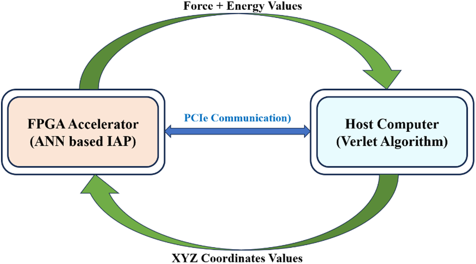
Figure 1: The hardware-software Co-design prototype for MD simulation
The prototype design shown in Fig. 1 divides the system into two parts. The FPGA hardware handles complex, time-intensive computations while the host computer manages controlling functions and sequential computations. The heterogeneous computing-based MD simulation shown in the model requires constant communication between the host computer and the FPGA board to function correctly. Peripheral Component Interconnect Express (PCIe) communication protocol is indeed used for communication between the FPGA and the host computer. In the hardware-software co-design shown in Fig. 1, the Cartesian coordinates (X, Y, and Z) are sent from the host computer to the FPGA, and the outputs (forces and energy values) are sent from the FPGA to the host computer using PCIe communication. Thus, in every MD cycle, around 3.5 KB (Kilobytes) of data transfer occurs between the FPGA and host computer using PCIe for Au147. With PCIe communication 50,000 MD cycles, PCIe took 19.84 h, whereas HPC Server took 29 h for Au147 nanoparticles. With PCIe, the computation time was reduced by 1.5 times as reported by Bulusu et al. [19].
Due to its high-speed serial point-to-point capabilities, PCIe is widely used in heterogeneous computing, especially in applications requiring large amounts of data transfer. However, PCIe comes with limitations. A thorough study by Marcin et al. [4] on FPGA applications highlights the first drawback, emphasizing the necessity for dedicated hardware and drivers, specifically a PCIe slot and associated drivers, leading to increased programming complexities. The second limitation involves the absence of support for hot plug operations, thus requiring a system restart for configuration. Also, PCIe’s complexity overhead is unnecessary for small data transfers like a few KBs (here, 3.5 KB for Au147 and 7.2 KB for Au309). Hence, the advantage of high-speed and low-latency data transfer is reduced due to the complexity overhead in a few KB data transfers.
This paper presents a novel approach to exploring UART (Universal Asynchronous Receiver/Transmitter) and Ethernet communication protocols for the same MD computation. We aim to reduce computation time further. Communication protocols like UART and Ethernet present versatile and user-friendly alternatives. Utilizing simplified, universally applicable code across operating systems helps mitigate the complexities associated with PCIe implementations. Both UART and Ethernet protocols support hot plug operations, eliminating the need for system restarts. These protocols are also easier to use than PCIe, and using them in embedded heterogeneous computing systems makes it easier to control the complete system by letting embedded processors step in. This attempt is for two atomic gold nanoparticles Au147 and Au309.
To reduce computation time, UARTLite and EthernetLite IP (Intellectual Property) are explored in the design with the following key setup:
1. Explore UART and Ethernet communication protocols as alternatives to PCIe communication for ANN-based MD simulation for gold nanoparticles.
2. Integrate the Microblaze soft-core processor to enhance hardware control ensuring an easily debuggable system.
3. Implement the MD calculation in the FPGA-Computer (CPU) based system using both communication protocols.
The paper is structured as follows: Section 2 outlines the system architecture overview. Section 3 discusses the hardware-software co-design for UART and Ethernet-based design implementation. The obtained results are presented in Section 4. Section 5 provides a detailed discussion, and Section 6 concludes the paper.
2 System Architecture Overview
The block diagram of hardware-software co-design for ANN-based MD simulation of gold nanoparticles is shown in Fig. 2. Several FPGA IPs have been used to design hardware in Xilinx Vivado. A brief overview of these IPs is given below.
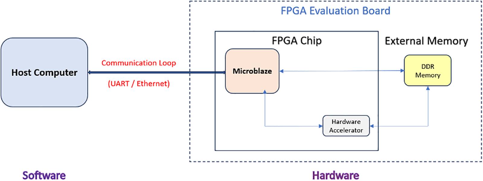
Figure 2: Block diagram of hardware-software Co-design for MD simulation
2.1.1 Microblaze: Soft-Core Processor
It is a 32-bit general-purpose Reduced Instruction Set Computer (RISC) soft-core processor. This processor features a 32-bit general-purpose register, RISC Harward Architecture, a 3-stage pipeline, and an interrupt module [21]. Utilizing the local memory bus (LMB), Microblaze accesses on-chip memory and is compatible with the IEEE 754 single-precision floating-point format. It also includes an Instruction Cache (IC) and Data Cache (DC), exception handling, a debug module, and a barrel shifter. Except for the Zynq family, Microblaze is supported in most Xilinx FPGA families (Artix-7, Kintex-7, Spartan, etc.). A comprehensive explanation of Microblaze is provided in XilinxMicroblaze [22].
Xilinx provides a software environment called Software Development Kit (SDK) with the Embedded processor (Microblaze) [22]. The SDK supports C/C++ languages for writing software code and is responsible for controlling the operation of the Microblaze soft-core processor. It extends support to all peripherals IPs used with the processor.
2.1.2 Communication IP (AXI UARTLite/EthernetLite)
The Advanced eXtensible Interface (AXI) UARTLite serves as a control interface for asynchronous serial data transfer. It supports full-duplex communication, providing AXI4-Lite interface register access and data transfer. The receiver and transmitter (First in First out) FIFO size are limited to 16 Bytes. This module incorporates configurable baud rates (e.g., 9600, 115200, 421800, 921600, etc.). A comprehensive explanation of AXI UARTLite is available in XilinxUart [23]. UARTLite IP follows the standard UART frame format as shown in Fig. 3. In this implementation, the parity bit is not used, and the stop bit size is one bit. Thus, each UART packet (frame) is 10 bits in size.
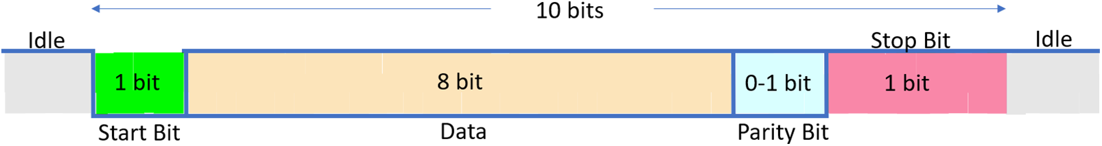
Figure 3: UART frame format
The AXI EthernetLite is designed to incorporate the features of the IEEE 802.3 Ethernet standard. It facilitates connection to external 10/100 Mb/s physical (PHY) transceivers through the Media Independent Interface (MII). It utilizes the AXI4/AXI4-Lite on-chip communication protocol to enable communication with the Microblaze soft-core Processor. A comprehensive explanation of the AXI EthernetLite is provided in XilinxEthernet [24]. EthernetLite IP follows the IEEE 802.3 standard Ethernet frame format for communication as shown in Fig. 4. This frame format allows a maximum of 1500 bytes of actual data to be sent, along with an additional 14 bytes for the header and 4 bytes for the Cyclic Redundancy Check (CRC). Therefore, for larger data sizes, multiple Ethernet frames have been used.

Figure 4: IEEE 802.3 ethernet frame format
2.2 Hardware Accelerator HLS IP for ANN-Based IAP Calculation
In this subsection, FPGA hardware blocks are introduced for reconfigurable high-performance computation. Generally, high-performance computation contains multiple loops. So, in conventional processors, all loops run sequentially. However, FPGA has the ability to take up several independent serial loops and can parallelize them [25]. So, when implemented on FPGA, similar tasks are performed concurrently, and the algorithm will be converted into multipliers and adders (MAC blocks) that go along multiple loops.
The Algorithm 1 [19] for constructing the ANN-based IAP for gold nanoparticles is described below. Firstly, obtaining cartesian coordinates from the host computer via UART/Ethernet communication. The cartesian coordinates are used to calculate radial and angular descriptors and their derivatives. The descriptors serve as input to the NN (Neural Network) to evaluate the energy for each atom. Force components are calculated using the derivatives of the descriptors. Finally, the force components are sent back to the host computer.

Vivado-HLS (High-Level Synthesis) software has been chosen to accelerate this high-performance computation algorithm. Utilizing C-based code in Vivado HLS, it was converted into Hardware Description Language (HDL). As shown in Fig. 5, after composing the C language code, the AXI_return directive was used to make it AXI-compatible. After that, a pipeline was applied to enhance the latency and throughput of the system. Also, all operations are floating-point operations and contain multidimensional arrays. So, it requires significant space in memory. Array partitioning directive is used to optimize multidimensional arrays. Upon achieving the optimal design, the algorithm was exported to the RTL (Register Transfer Level) design and then converted into IP. The physics and mathematical calculations of this module are completely discussed in Bulusu et al. [19].

Figure 5: Design flow for HLS IP creation
The inputs of the proposed system are (X, Y, Z) cartesian coordinates of atoms and the outputs are forces and total energy of the nanoparticles. Thus, data being large, are stored in the DDR (Double Data Rate) memory present in the FPGA evaluation board. Microblaze, a microcontroller IP was used to control data from the host computer to memory and vice-versa. Fig. 6 shows the sequence of data transfer for one single operation.
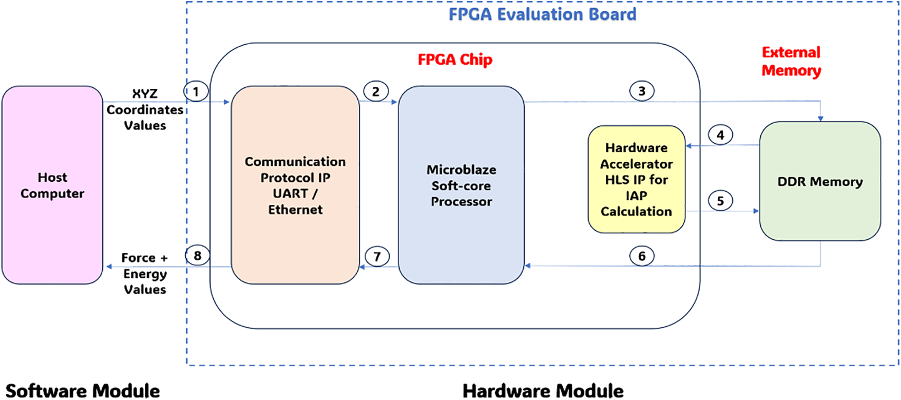
Figure 6: Data flow diagram of system implementation for MD simulation
The complete FPGA implementations of UART and Ethernet communication-based heterogeneous computing systems are discussed in detail in the following subsection.
3.1 IAP Implementation Using UART/Ethernet
To design a communication interface, a schematic-based design was developed in Xilinx Vivado as shown in Fig. 4 hardware module [26]. This design included DDR3 (Double Data Rate3) SDRAM (Synchronous Dynamic Random-Access Memory) on the Kintex KC-705 board for data storage during processing. The Microblaze soft-core processor acted as the master controller, operating at 300 MHz, while the hardware accelerator MD simulation IP operated at 100 MHz. Communication between the FPGA and the host computer was handled by the AXI UARTLite IP / EthernetLite IP. Other Peripheral IPs communicated with the Microblaze processor through AXI Interconnect or SmartConnect IP.
An Embedded-C language code was written in Xilinx SDK to control the hardware [27]. This code handled tasks such as data reception and transmission, data storage in DDR memory, and initiation and termination of the hardware accelerator module. The flowchart of the SDK code is shown in Fig. 7. The structure of the SDK code is nearly identical for UART and Ethernet-based designs. Changes related to communication interfaces were highlighted with different colored rectangular dotted boxes, with an orange box denoting UART communication and a green box for Ethernet communication.

Figure 7: SDK flow diagram for UART and ethernet communication implementation
The entire IAP computation is implemented as a hardware-software co-design. The Microblaze acts as a master and the hardware accelerator IP serves as a slave. The Microblaze starts with a polling to expect ‘X, Y, Z’ coordinates values from the computer. Upon receiving the same, the accelerator IP is activated and the Microblaze goes into SLEEP mode. Parallelly, it will initiate another polling mode to wait for the forces & energy deposition with the memory.
The accelerator IP uses the parallel algorithm on the FPGA to calculate the forces & energy and deport the same in the DDR memory. Further, it ends the wait for the Microblaze. The Microblaze gets activated and transfers the data through UART/Ethernet IP to the host computer. Depending on the number of cycles, the entire process is repeated.
The Verlet algorithm was used to execute the remaining sequential operations and compile all necessary MD files in the host computer. The C-program in the host computer manages the UART/Ethernet communication between the host computer and FPGA.
For performing the MD simulation, two different examples are explored. They are Au147 and Au309 nanoparticles. The FPGA used was Xilinx Kintex-7 KC-705 evaluation FPGA board. In addition to the accelerator IP developed, a Microblaze-based microcontroller system was also implemented through the block design of the Xilinx Vivado software. The accelerator outputs energy and force values which need to be transferred to the computer. A separate Verlet algorithm will take the force and energy values and calculate the next set of coordinates on the computer side. The accelerator IP on the FPGA works at 100 MHz, while the Microblaze processor and its peripherals operate at 300 MHz. For communicating between the FPGA and the computer, AXI UARTLite and AXI EthernetLite IPs were implemented. Microblaze processor controls the data transfer between the FPGA Random Access Memory (RAM) and the different communication IPs, and this program was written in embedded C.
The first step in this exploration is to identify the accuracy of the results obtained through the proposed communication strategies. The calculated energy for every MD cycle from the FPGA-based heterogeneous computing system should match the conventional approach (using a server). To check the accuracy, both UART and Ethernet-based communication were implemented, and the MD simulations were run on the board for 500 cycles. The results of energy and forces obtained at every cycle were compared with a conventional approach, and the results are plotted in Fig. 8. There is no difference between the results obtained from all the approaches, and this proves that the proposed approach yields accurate results for several cycles as well. It validates that the total potential energy obtained using UART and Ethernet designs is correct and identical to the PCIe-based design and HPC server, as explained in Bulusu et al. [19].
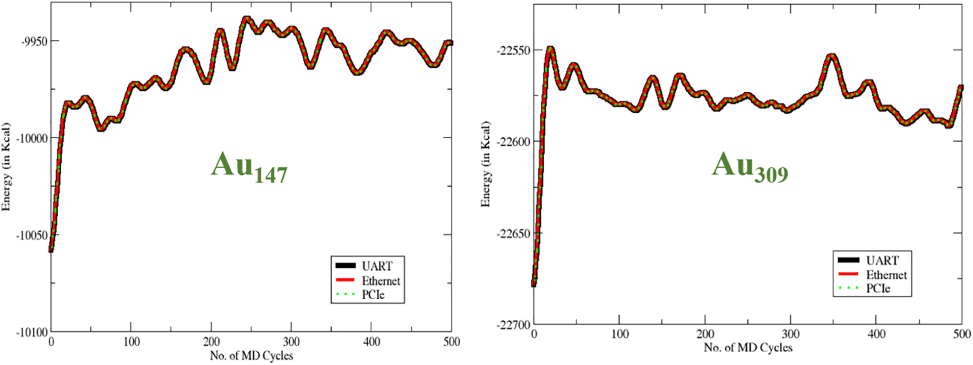
Figure 8: Potential energy of Au147 & Au309 vs. number of MD cycles
Now that the accuracy of the system is verified, the system was explored to determine the computation time for the two different communication protocols implemented onto the FPGA board. A comparison of the computation time of the proposed two communication approaches with the conventional PCIe and HPC server is shown in Table 1. UART operates at a baud rate of 921,600 bits/sec, while Ethernet works at a standard speed of 100 Mb/sec. PCIe speed is noted as 5 GT/sec, and in the HPC server, seven CPUs run in parallel at a frequency of 2600 MHz (Megahertz). Interestingly, UART and Ethernet-based communication protocols can withstand 50,000 iterations of MD computations, and the time it takes for 50,000 iterations comes to 17.54 & 18.7 h for UART & Ethernet communication, respectively for Au147 and 64.36 & 65.56 h respectively for Au309. This shows the robustness of the system and the potential to provide a lab-on-a-chip solution for such IAP computations.
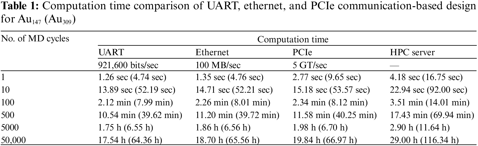
Initially, X, Y, and Z values were sent to the FPGA and the returning data were the computed force and energy values. For the Au147 atoms, 442 32-bit numbers (147 force values in each X, Y, and Z direction + 1 total energy value) were transmitted from the memory to the computer. The return communication was 441 32-bit numbers back to the FPGA. In such cases, the total data transfer was 3.5 KB per cycle. Even though PCIe communication is faster, the overheads (e.g., frame construction) and loading of the drivers take more time. It is interesting to note that UART and Ethernet communication can achieve better computational efficiency compared to PCIe communication, despite PCIe being faster.
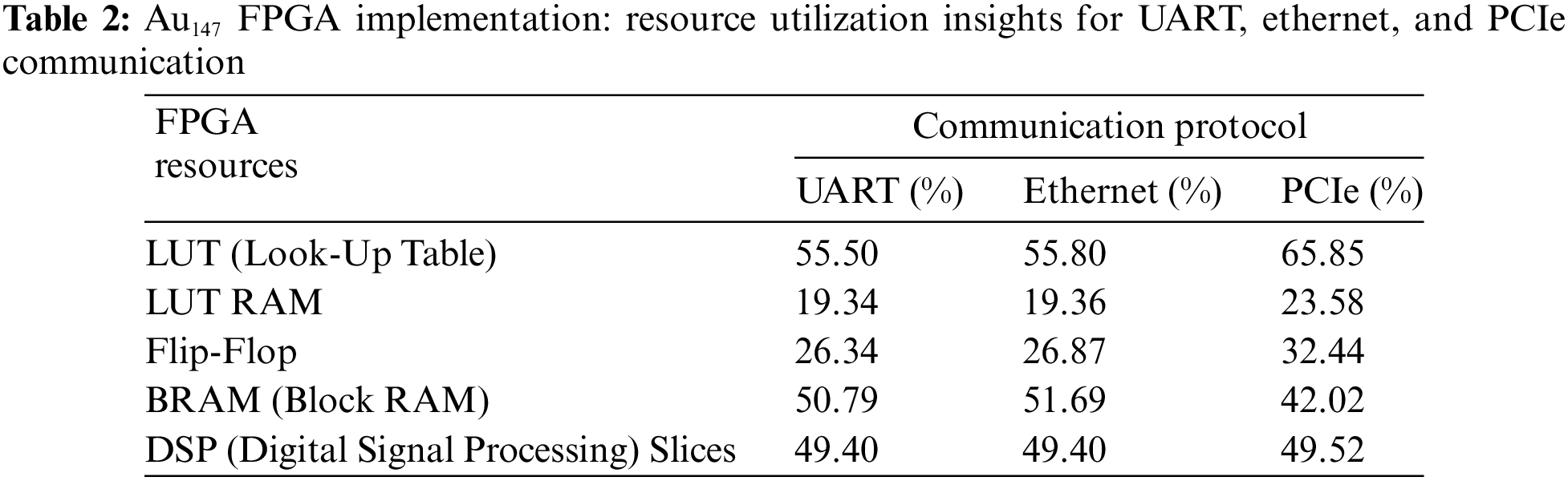
The next step is to determine the resources used by the FPGA board in both communication approaches. This has a direct correlation to the power of the system. The results, as tabulated in Table 2, reveal that the UART and Ethernet designs, leveraging a Microblaze soft-core processor, demonstrate lower overall resource utilization than the PCIe-based design.
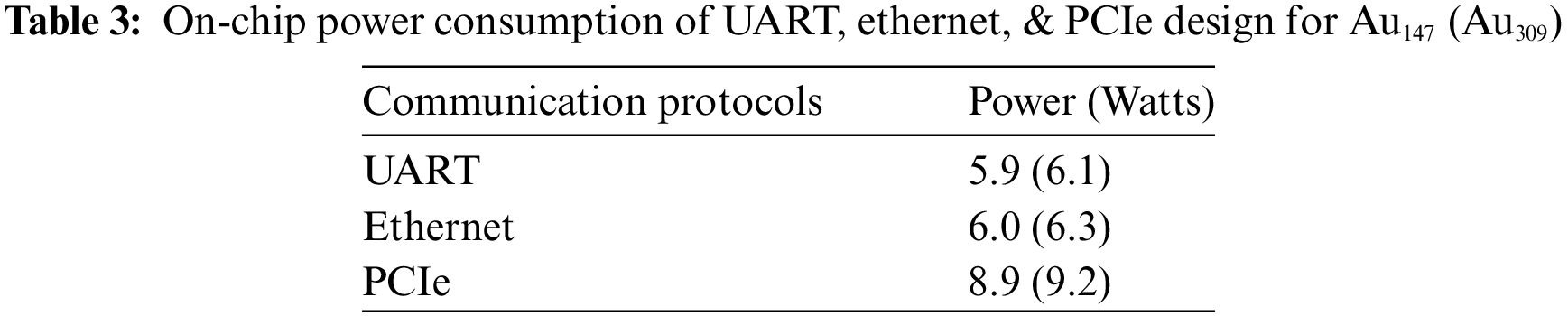
For a Lab-on-a-chip application, power consumption plays a very important role. Table 3 shows the power consumed by the different communication protocols. It is clear that UART consumes the least power, followed by the other protocols. This again can be attributed to the simplicity of the communication protocols.
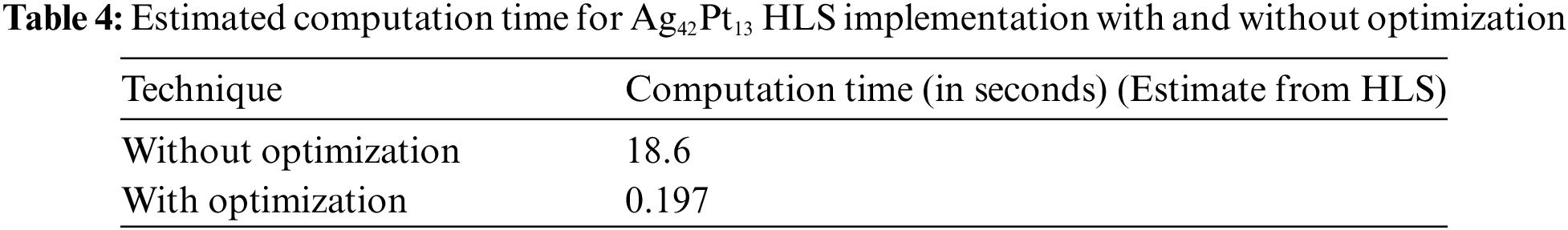
To check the efficiency of the proposed setup to experiment on new systems, an exploration Ag42Pt13 system was explored. This system utilized the same feed-forward ANN model (59-30-30-1). However, since this alloy consists of two types of nanoparticles in the atomic cluster, the HLS code was modified with several additional conditional statements and loops. The algorithm for this system was written in an HLS-based FPGA program and the latency and the estimated computation time were calculated from the HLS synthesis. Table 4 shows the details of the estimated time before and after parallel operations. It is clear from this table that the proposed system can provide a significant reduction in computation time for up to two orders.
The communication speeds of UART and Ethernet (100 ×
While the packet size of UART is 10 bits of communication (8 bits of actual data), ethernet and PCIe communication communicates with several initial frames and library initialization. The reason behind such a contradictory result could be ascertained by estimating the overheads of these communication protocols. Needless to say, that UART has minimal overhead and can be considered negligible compared to its own communication speed.
Ideally, one complete cycle of the MD calculation with any communication protocol is a combination of computation and communication time. This is shown in Eq. (1) below:
where
❖ Au147 Time Calculations:
In the case of UART Communication for 1 cycle,
From Eq. (1),
In case of Ethernet Communication for 1 cycle,
From Eq. (1) we know that
From the above analogy, it is very clear that to find the tipping point where Ethernet communication will have a better hand compared to UART, the accountability of overhead of 0.032 s should be looked into. With these overheads in mind, one can propose which communication protocol should be used and can be predicted with simple calculations. The tipping point occurs when the time taken in 1 cycle using UART is same as the time taken in 1 cycle using Ethernet in transferring some data. This can be shown as
In Eq. (11), we omitted
To explain it experimentally, Table 5 shows
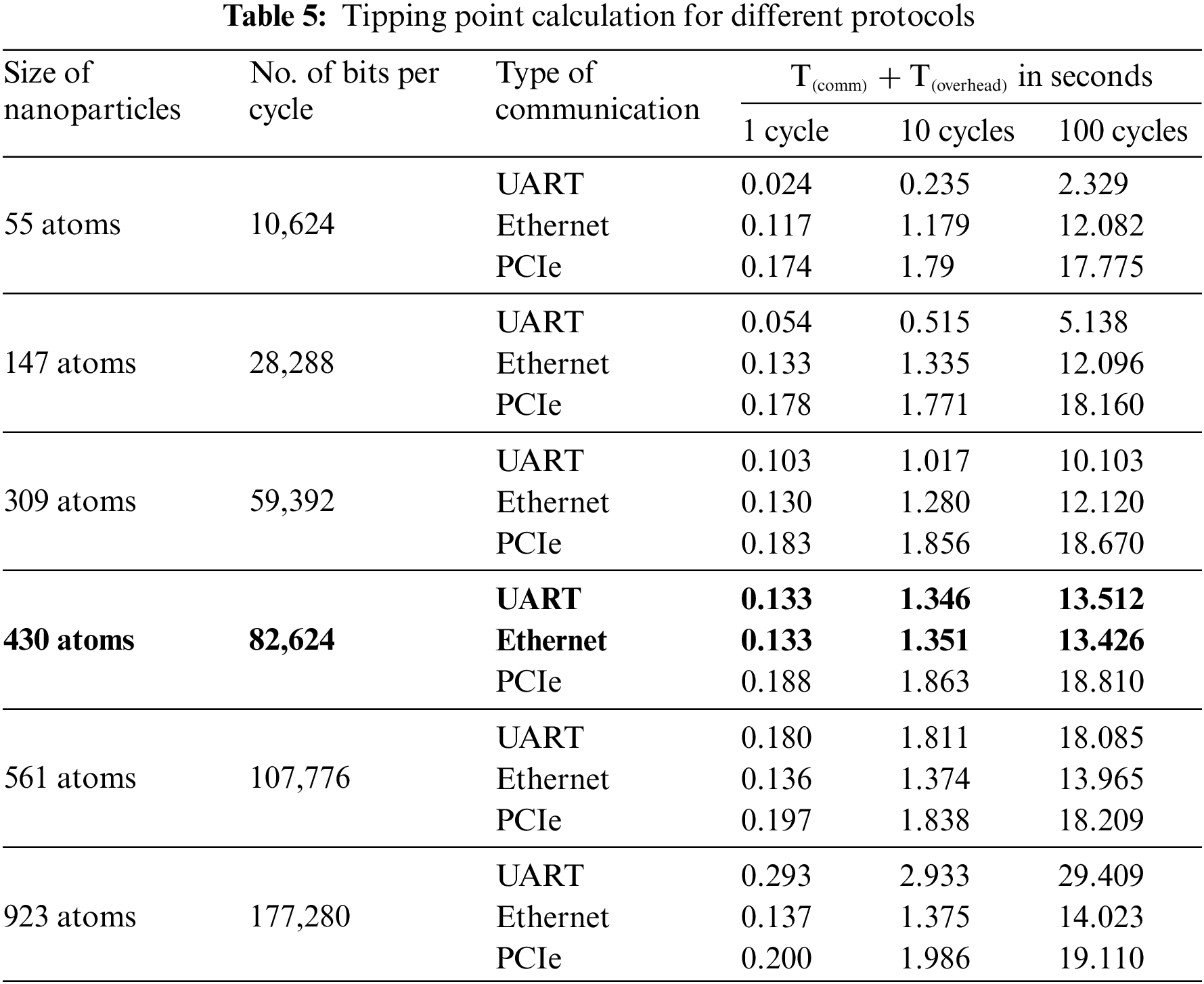
The ANN-based MD Simulation for Au147 and Au309 was implemented on the Xilinx Kintex-7 KC705 evaluation FPGA board. A hardware accelerator module with new communication strategies is proposed and implemented for 50,000 MD cycles. The computation time for 50,000 MD cycles is 17.54 and 18.7 h for UART and Ethernet communication, respectively for Au147 and 64.36 & 65.56 h respectively for Au309. Compared to the conventional HPC server, the proposed methodology has improved the computation time by 1.65 (1.81) times in UART and 1.55 (1.77) times in Ethernet communication for Au147 (Au309) nanoparticles. The actual MD simulation requires more than 1 million cycles, so this computation time difference becomes more significant. The proposed systems significantly reduce resource utilization, resulting in decreased on-chip power consumption. In the implemented system, on-chip power consumption measured from Xilinx Vivado was 5.9 (6.1) Watts for UART and 6.0 (6.5) Watts for Ethernet, respectively, for Au147 (Au309). Compared to conventional PCIe, on-chip power is reduced by 33% and 32% in UART and Ethernet, respectively. From this, we concluded that where the nanoparticle size is larger than 430 atoms, Ethernet communication is preferable in comparison to UART and PCIe and if the nanoparticle size is less than 430 atoms, then UART is more efficient. Both UART and Ethernet communication are robust, hot-pluggable, and user-friendly. This can lead to low-cost HPC for students and researchers to explore nanoparticles of experimental relevance. This application paves the way for the development of a Lab-on-a-Chip platform for the computation of IAP in the future.
Acknowledgement: Ankitkumar Patel thanks Kishore Reddy Kurapati and Dharmendra Kartikey for their valuable suggestions and discussions during this research. The authors also extend their thanks to Kritika Bhardwaj for providing assistance related to PCIe work. Additionally, Ankitkumar Patel acknowledges IIT Indore for providing research fellowship and facilities.
Funding Statement: The authors received no specific funding for this study.
Author Contributions: Ankitkumar Patel: Investigation, Data collection, Methodology, Analysis and Results interpretation, Draft manuscript preparation. Srivathsan Vasudevan: Project Design and Proposal, Conceptualization, Resources, Supervision, Validation, Draft review and editing. Satya Bulusu: Project Design and Proposal, Conceptualization, Resources, Supervision, Validation, Draft review and editing. All authors reviewed the results and approved the final version of the manuscript.
Availability of Data and Materials: Not applicable.
Ethics Approval: Not applicable.
Conflicts of Interest: The authors declare that they have no conflicts of interest to report regarding the present study.
References
1. L. Bin, Z. Dawid, S. Henry, and G. Laxmi, “Accelerating high performance computing applications: Using CPUs, GPUs, Hybrid CPU/GPU, and FPGAs,” in Proc. 13th Int. Conf. PDCAT, Beijing, China, Dec. 2012, pp. 337–342. [Google Scholar]
2. L. Xu, O. Hibat-Allah, G. Abdelouahed, W. Li, and C. Mohamed, “A hybrid GPU-FPGA based design methodology for enhancing machine learning applications performance,” J. Ambient Intell. Humaniz. Comput., vol. 11, no. 6, pp. 2309–2323, Jun. 2020. doi: 10.1007/s12652-019-01357-4. [Google Scholar] [CrossRef]
3. V. Mario and N. Horacio, “Trends of CPU, GPU and FPGA for high-performance computing,” in Proc. 24th Int. Conf. FPL, Munich, Germany, Sep. 2014, pp. 1–6. [Google Scholar]
4. K. Marcin and D. Grzegorz, “Simple communication with FPGA device over ethernet interface,” in Proc. 20th Int. Conf. CN, Lwowek Slaski, Poland, Jun. 2013, pp. 290–299. [Google Scholar]
5. Y. Li, X. Zhao, and T. Cheng, “Heterogeneous computing platform based on CPU+FPGA and working modes,” in Proc. 12th Int. Conf. CIS, Wuxi, China, Dec. 2016, pp. 669–672. [Google Scholar]
6. L. Shi, H. Chen, J. Sun, and K. Li, “vCUDA: GPU-accelerated high-performance computing in virtual machines,” IEEE Trans. Comput., vol. 61, no. 6, pp. 804–816, Jun. 2011. doi: 10.1109/TC.2011.112. [Google Scholar] [CrossRef]
7. J. Fang, K. Zhou, M. Y. Zhang, and W. Xiang, “Resource scheduling strategy for performance optimization based on heterogeneous CPU-GPU platform,” Comput. Mater. Contin., vol. 73, no. 1, pp. 1621–1635, Jun. 2022. doi: 10.32604/cmc.2022.027147. [Google Scholar] [CrossRef]
8. M. Herbordt et al., “Achieving high performance with FPGA-based computing,” Computer, vol. 40, no. 3, pp. 50–57, Mar. 2007. doi: 10.1109/MC.2007.79. [Google Scholar] [PubMed] [CrossRef]
9. S. Jindal, S. Chiriki, and S. Bulusu, “Spherical harmonics based descriptor for neural network potentials: Structure and dynamics of Au147 nanocluster,” J. Chem. Phys., vol. 146, no. 20, 2017, Art. no. 3168. doi: 10.1063/1.4983392. [Google Scholar] [PubMed] [CrossRef]
10. G. Helmut, H. Helmut, W. Andreas, and S. Klaus, “Generalized Verlet algorithm for efficient molecular dynamics simulations with long-range interactions,” Mol. Simul., vol. 9, no. 1–3, pp. 121–142, Jun. 1991. doi: 10.1080/08927029108022142. [Google Scholar] [CrossRef]
11. M. Nicos and M. Raymond, “Velocity Verlet algorithm for dissipative-particle-dynamics-based models of suspensions,” Phys. Rev. E, vol. 59, no. 3, pp. 3733–3736, Mar. 1999. doi: 10.1103/PhysRevE.59.3733. [Google Scholar] [CrossRef]
12. S. Pál et al., “Heterogeneous parallelization and acceleration of molecular dynamics simulations in GROMACS,” J. Chem. Phys., vol. 153, no. 13, pp. 121–142, Oct. 2020. doi: 10.1063/5.0018516. [Google Scholar] [PubMed] [CrossRef]
13. D. Jones et al., “Accelerators for classical molecular dynamics simulations of biomolecules,” J. Chem. Theory Comput., vol. 18, no. 7, pp. 4047–4069, Jun. 2022. doi: 10.1021/acs.jctc.1c01214. [Google Scholar] [PubMed] [CrossRef]
14. N. Kondratyuk, V. Nikolskiy, D. Pavlov, and V. Stegailov, “GPU-accelerated molecular dynamics: State-of-art software performance and porting from Nvidia CUDA to AMD HIP,” Int. J. High Perform. Comput. Appl., vol. 35, no. 4, pp. 312–324, Apr. 2021. doi: 10.1177/10943420211008288. [Google Scholar] [CrossRef]
15. Y. Chen et al., “Fully integrated FPGA molecular dynamics simulations,” in Proc. SC 19 Int. Conf. High Perform. Comput., Netw., Storage, Anal., New York, NY, USA, Nov. 2019, pp. 1–31. [Google Scholar]
16. Z. Li, Q. Li, H. Liu, and Z. Zhao, “FPGA optimized accelerator of DCNN with fast data readout and multiplier sharing strategy,” Comput. Mater. Contin., vol. 77, no. 3, pp. 3237–3263, Dec. 2023. doi: 10.32604/cmc.2023.045948. [Google Scholar] [CrossRef]
17. S. Ronald, G. Maya, T. Frans, and P. Viktor, “Hardware/software approach to molecular dynamics on reconfigurable computers,” in 2006 14th Annual IEEE Symp. Field-Programmable Custom Comput. Mach., Napa, CA, USA, IEEE, 2006. Accessed: Jan. 20, 2024. [Online]. Available:https://ieeexplore.ieee.org/abstract/document/4020892 [Google Scholar]
18. C. Pascoe, L. Stewart, B. Sherman, V. Sachdeva, and M. Herbordt, “Execution of complete molecular dynamics simulations on multiple FPGAs,” in Proc. IEEE Conf. High Perform. Extreme Comput. (HPEC), Waltham, MA, USA, Sep. 22–24, 2020, pp. 1–2. [Google Scholar]
19. S. Bulusu and S. Vasudevan, “FPGA accelerator for machine learning interatomic potential-based molecular dynamics of gold nanoparticles,” IEEE Access, vol. 10, pp. 40338–40347, Apr. 2022. doi: 10.1109/ACCESS.2022.3165650. [Google Scholar] [CrossRef]
20. Inc Xilinx, “KC705 evaluation board for the Kintex-7 FPGA user guide,” version: UG810 v1.9, USA, Feb. 4, 2019. Accessed: Mar. 13, 2023. [Online]. Available: https://docs.amd.com/v/u/en-US/ug810_KC705_Eval_Bd [Google Scholar]
21. T. Jason, I. Anderson, and K. Mohammed, “Soft-core processors for embedded systems,” in Proc. Int. Conf. Microelectron. (ICM), Dhahran, Saudi Arabia, Sep. 2006, pp. 170–173. [Google Scholar]
22. Inc Xilinx, “MicroBlaze processor reference guide,” version: UG984 v2021.2, USA, Oct. 27, 2021. Accessed: Nov. 15, 2022. [Online]. Available: https://www.xilinx.com/content/dam/xilinx/support/documents/sw_manuals/xilinx2021_2/ug984-vivado-microblaze-ref.pdf [Google Scholar]
23. Inc Xilinx, “AXI UART Lite LogiCORE IP product guide,” version: PG142 v2017. 2, USA, Apr. 5, 2017. Accessed: Dec. 6, 2022. [Online]. Available: https://docs.amd.com/v/u/en-US/pg142-axi-uartlite [Google Scholar]
24. Inc Xilinx, “AXI Ethernet lite MAC LogiCORE IP product guide,” version: PG135 v2021. 3, USA, Nov. 2, 2021. Accessed: Feb. 2, 2023. [Online]. Available: https://docs.amd.com/r/en-US/pg135-axi-ethernetlite/AXI-Ethernet-Lite-MAC-v3.0-LogiCORE-IP-Product-Guide [Google Scholar]
25. M. Gokhale and L. Shannon, “FPGA Computing,” IEEE Micro, vol. 41, no. 4, pp. 6–7, Jul. 2021. doi: 10.1109/MM.2021.3088975. [Google Scholar] [CrossRef]
26. Inc Xilinx, “Vivado design suite user guide: Embedded processor hardware design,” version: UG898 v2021.1, USA, Jun. 16, 2021. Accessed: Jan. 17, 2023. [Online]. Available: https://docs.amd.com/v/u/2021.1-English/ug898-vivado-embedded-design [Google Scholar]
27. Inc Xilinx, “UltraFast embedded design methodology guide,” version: UG1046 v2018.2.3, USA, Apr. 20, 2018. Accessed: Aug. 6, 2023. [Online]. Available:https://docs.amd.com/v/u/en-US/ug1046-ultrafast-design-methodology-guide [Google Scholar]
Cite This Article
 Copyright © 2024 The Author(s). Published by Tech Science Press.
This work is licensed under a Creative Commons Attribution 4.0 International License , which permits unrestricted use, distribution, and reproduction in any medium, provided the original work is properly cited.
 Downloads
 Citation Tools