
 Submit a Paper
 Propose a Special lssue
 Open Access
ARTICLE
CNN Accelerator Using Proposed Diagonal Cyclic Array for Minimizing Memory Accesses
1 Department of Electronics, College of Electrical and Computer Engineering, Chungbuk National University, Cheongju, 28644, Korea
2 Department of Electrical Engineering, College of Engineering, Al-Azhar University, Cairo, 11651, Egypt
* Corresponding Author: Hyung-Won Kim. Email:
Computers, Materials & Continua 2023, 76(2), 1665-1687. https://doi.org/10.32604/cmc.2023.038760
Received 28 December 2022; Accepted 12 April 2023; Issue published 30 August 2023
 View Full Text
 Download PDF
Abstract
This paper presents the architecture of a Convolution Neural Network (CNN) accelerator based on a new processing element (PE) array called a diagonal cyclic array (DCA). As demonstrated, it can significantly reduce the burden of repeated memory accesses for feature data and weight parameters of the CNN models, which maximizes the data reuse rate and improve the computation speed. Furthermore, an integrated computation architecture has been implemented for the activation function, max-pooling, and activation function after convolution calculation, reducing the hardware resource. To evaluate the effectiveness of the proposed architecture, a CNN accelerator has been implemented for You Only Look Once version 2 (YOLOv2)-Tiny consisting of 9 layers. Furthermore, the methodology to optimize the local buffer size with little sacrifice of inference speed is presented in this work. We implemented the proposed CNN accelerator using a Xilinx Zynq ZCU102 Ultrascale+ Field Programmable Gate Array (FPGA) and ISE Design Suite. The FPGA implementation uses 34,336 Look Up Tables (LUTs), 576 Digital Signal Processing (DSP) blocks, and an on-chip memory of only 58 KB, and it could achieve accuracies of 57.92% and 56.42% mean Average Precession @0.5 thresholds for intersection over union (mAP@0.5) using quantized 16-bit and 8-bit full integer data manipulation with only 0.68% as a loss for 8-bit version and computation time of 137.9 and 69 ms for each input image respectively using a clock speed of 200 MHz. These speeds are expected to be doubled five times using a clock speed of 1 GHz if implemented in a silicon System on Chip (SoC) using a sub-micron process.Keywords
CNNs are among the most popular neural network structures increasingly adopted in deep learning image recognition and processing. The research on CNNs has enabled countless applications, and it accomplished phenomenal improvement in accuracy [1]. However, the complexity of modern CNN structures is rapidly increasing due to the mounting number of arithmetic computations and memory accesses. Real-time applications of CNNs, especially for mobile applications, require accelerators with higher execution speeds at lower power consumption. The main challenges for designing a CNN hardware accelerator are the limited bandwidth and resources [2]. The proposed DCA could achieve a remarkable reduction regarding memory access. The FPGA-based accelerators that improve the performance and energy efficiency of the computation-demanding CNN became an attractive alternative [3]. Enabling the balance of parallel computing while reducing system power consumption could be achieved by utilizing an innovative kernel partition technique that reduces feature maps and kernel data repetition [4]. Due to bandwidth issues and small on-chip memory size, the performance of CNN FPGA-based accelerators is limited. Based on extensive analysis of CNN models, the convolutional layers are computationally centric. At the same time, accessing is much more critical in fully connected memory, so in this case, the dynamic-precision data quantization and an effective hardware design can solve bandwidth issues and improve resource utilization [5]. Furthermore, a hardware-friendly quantization uses only integer arithmetic with power-of-two scale factors to replace multiplication and division operations with shift operations can be utilized to reduce the memory footprint and complexity of computations [6].
To improve the speed and efficiency of Convolutional Neural Networks (CNNs), researchers have proposed various CNN accelerators that utilize specialized hardware architectures. These accelerators typically consist of numerous parallel Processing Element (PE) units. Each PE comprises a Multiplier and Accumulator (MAC), which is heavily utilized in implementing CNN operations. The goal of accelerator design is generally to maximize the utilization of the PEs. The authors in [7] proposed a configurable (interleaved/elementwise for the input data) vector-wise 1-D 3 × 3 filter CNN accelerator. This low-area design could achieve 99% hardware utilization for VGG-16. A low latency accelerator architecture is proposed in [8], with padding skip a fine-grained column-based pipeline could reduce the pipeline start-up time. Also, to shrink the computational time, they introduced a double signed-multiplication correcting circuit. Furthermore, a shared buffer for the pooling unit was proposed to reduce storage costs. As a result, they could minimize accelerator latency to (2.125×∼2.34×) compared to previous work, increase the DSP efficiency up to 95.2%, and shrink 20.7% for BRAM consumption, all previous results for the YOLOv2-tiny CNN model. An acceleration for various types of neural networks was proposed in [9]. In this case, only network description files and input images are required. They used the dynamic fixed-point for network quantization. For SqueezeNet accelerating, they got 0.054GOPS/DSP as performance density and 5.24GOPS/W as power efficiency. Special array architectures have been studied to efficiently utilize PE units. Systolic Array architectures have been used to reuse the data and weight parameters and reduce repeated memory accesses [10–13]. Many research works employed this architecture and reported reduced memory access and power consumption [14–28]. For example, the work [14] used a systolic array without a multiplier to reduce hardware resources. The work [15] introduced a 3D architecture of a systolic array to reduce memory accesses. Several studies have proposed architectures for CNN accelerators that aim to minimize overall latency by propagating data and parameters and accumulated results within the Processing Element (PE) units to maximize data reuse [16–18]. There has also been an effort to reduce the on-chip memory size, such as input data memory size. When conducting convolution operation with a large input image, upper layers require a large memory due to large input data, but deeper layers often require smaller memory due to decreasing feature map size. This property causes a problem of memory size mismatch for most of the architectures reusing the same memory for multiple layers. Multiple studies have proposed partitioning large input images and feature maps [14–18] to address this issue. Although this method can reduce the memory size, it requires additional data reloading from Dynamic Random Access Memory (DRAM), causing a loss of data reuse efficiency. Furthermore, as the number of needed PEs increases to achieve the speed goal for a given clock speed, the utilization of PE hardware resources decreases. Most accelerator designs take weight parameters from the training process conducted by the CNN software model that usually uses floating point (FP) operations. However, FP operations’ initial weight and feature map data lead to excessive chip size and power consumption. Therefore, optimal quantization of weight and feature map data is vital for minimizing the chip size and power consumption. Many research works address quantization methods for accelerator designs [2–6,16–18,27–29]. In this paper, we proposed some modifications to optimize Yolov2-tiny. For further optimization, the trained model batch normalization parameters have been folded into only weights and biases, which facilitate the implementation process. Furthermore, the flooded floating-point parameters and activations were quantized to an 8-bit integer.
This paper proposes the following architecture components to meet the goal of smaller memory, fewer repeated memory accesses, and lower hardware resources.
• Diagonal Cyclic Array Architecture is a novel systolic array structure that recycles the data through diagonal cyclic paths through an array of PEs in a way that maximizes the data reuse rate and the computation speed.
• In Data Recycle First In First Out (FIFO) Architecture, a group of FIFOs inserts retrieved data to the next stage FIFO in a rotating position for data recycling. For n × n convolutional kernel, n − 1 FIFOs and a register are employed. For example, if the kernel size is 3 × 3, 2 FIFOs and one register are used.
• Integrated Post-Convolution Process, an integrated computation architecture for the activation function, max-pooling, and scaling function after convolution calculation, further reduces the hardware resource.
• Hierarchical Iteration Controller, an adaptive iteration controller that allows maximal reuse of DCA by hierarchical iterations for input channels, feature map slices, and output channels, offers flexibility to support various CNN.
• Weight Parameter Quantization, to reduce hardware cost and inference execution time, the trained the 32-bit floating-point model that was optimized by folding its batch normalization parameters and swapping the max pooling with activation functions. This optimization reduced 75% of all activation operations in the first five layers. The optimized 32-bit floating-point parameters were quantized into an 8-bit integer.
The rest of this paper is organized as follows. Section 2 introduces the overall architecture of the proposed CNN accelerator, while Section 3 describes Diagonal Cyclic Array and demonstrates its advantages. Also, it describes Post-Convolution Process and introduces. Section 4 presents the hierarchical iteration operation of the proposed architecture. Section 5 discusses the methodology for 8-bit weight quantization. Finally, Section 6 demonstrates the implementation and measurement results, followed by conclusions.
2 Overall Architecture of Proposed Accelerator
Fig. 1 illustrates the overall architecture of the proposed CNN accelerator. It consists of arrays of Processing Elements (PEs) called DCA, data recycle FIFOs for input buffer, global input buffer fetching a slice of input data for concurrent input channels Conv-Mem, a memory storing convolution results integrated Post-Convolution Process (PCP) blocks that calculate Pooling, Normalization, Activation function, and Output Memories storing the final results for individual output channels.
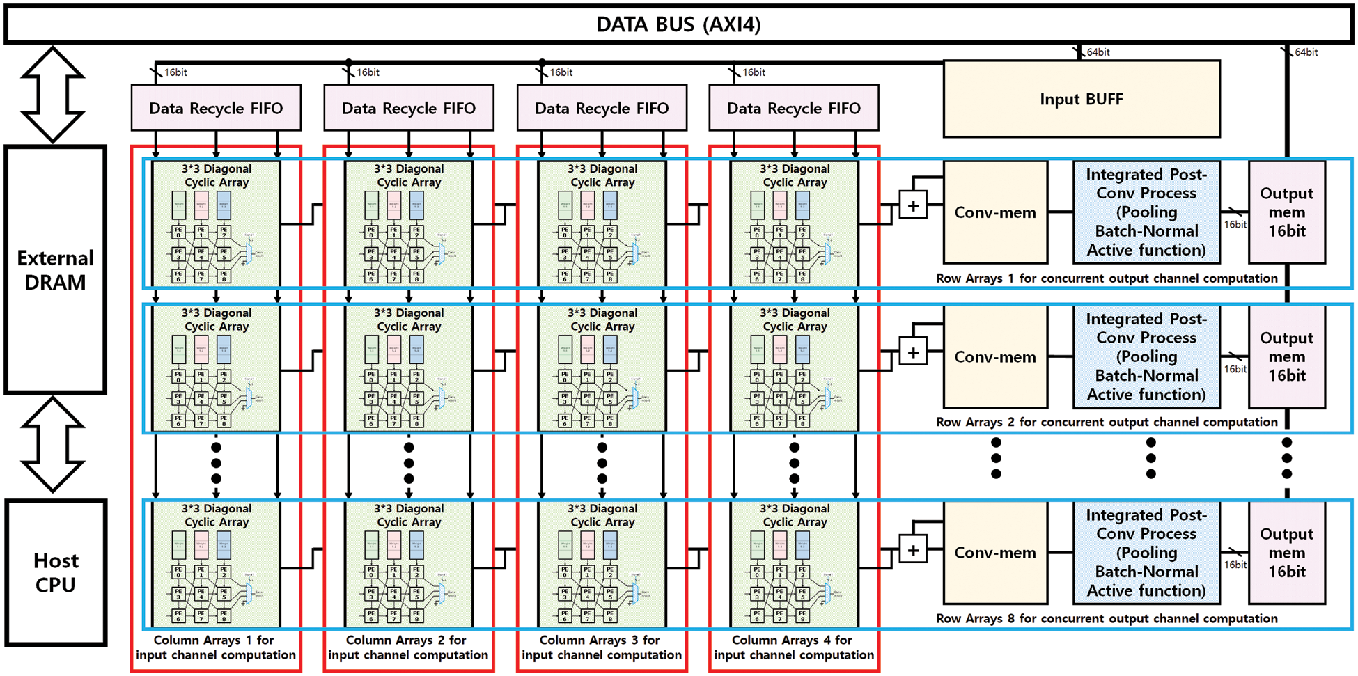
Figure 1: Proposed accelerator architecture
The accelerator receives data and weight parameters from external DRAM with a DRAM Controller through a 64-bit AXI4 system bus. The accelerator requires only compact on-chip memories, a global input buffer, and output memories for concurrent output channels, which communicate with the external DRAM. The flowchart in Fig. 2 explains the proposed accelerator processing steps, and the proposed accelerator configuration parameters can be found in Table 1.
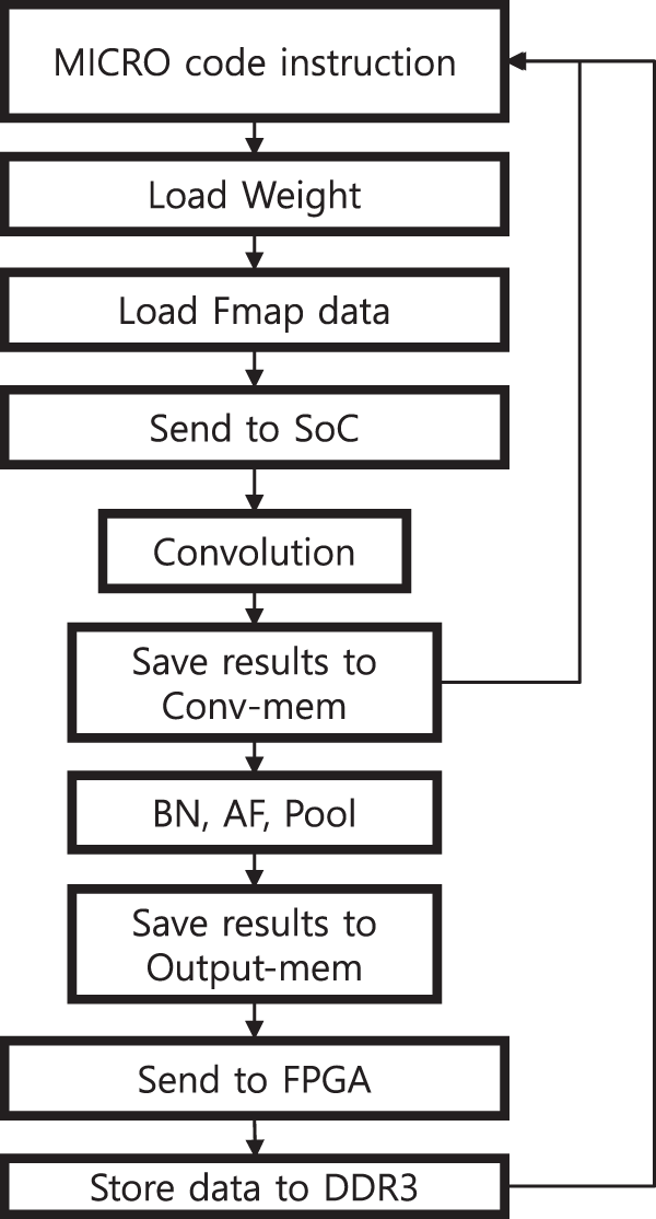
Figure 2: Proposed accelerator flowchart

2.1 The Proposed Diagonal Cyclic Array
This study proposes a novel Systolic Array called DCA. DCA takes sequential input data and weight parameters from the global input memory. Then it processes Convolution filter calculation by propagating the weight parameters in the vertical direction and the input data in the horizontal direction. Inside a DCA, each PE computes a MAC result and propagates it in the diagonal direction through cyclic paths of the array. In most of the existing systolic array architectures, each PE implements a complete convolution filter calculation iteratively. In the proposed DCA, in contrast, a string of PEs formed along each diagonal cyclic path implements each convolution filter calculation in cooperation. The proposed DCA is composed of two levels of arrays: Upper array represents concurrent channel level operations, which consists of M rows × N columns in Fig. 1. Here, M indicates the number of concurrent output channels calculated simultaneously in one iteration, whereas N denotes the number of concurrent input channels processed simultaneously in one iteration. The lower layer represents kernel-level operations, which comprise a sub-array for each M × N component in the upper array. A sub-array comprises K × K PEs, where K indicates the convolution kernel size. For example, suppose the target CNN model needs a (5 × 5) kernel. In that case, we can configure the sub-array to 5 × 5 PEs as illustrated in Fig. 3. In this paper, to demonstrate the structure and operation of DCA, an implementation example of CNN accelerator for YOLOv2-Tiny which uses 3 × 3 convolutional kernels in all nine layers leading to a sub-array of size 3 × 3 (K = 3). In the example implementation, we chose a DCA consisting of 8 rows × 4 columns = 32 kernel-level sub-arrays. The M = 8 rows of the 32 sub-arrays produce eight concurrent output channels, while the N = 4 columns of the 32 sub-arrays can take four input channels from the global input memory and compute their convolution kernels simultaneously. Since the above DCA implementation simultaneously produces eight output convolution filter results for the concurrent output channels, Conv-Mem consists of eight parallel local memories to store the eight outputs. For the same reason, PCP Block consists of eight parallel structures that concurrently calculate pooling, batch normalization, and activation functions for the eight output channels. The final result of the output Channels is stored in Output Buffer.
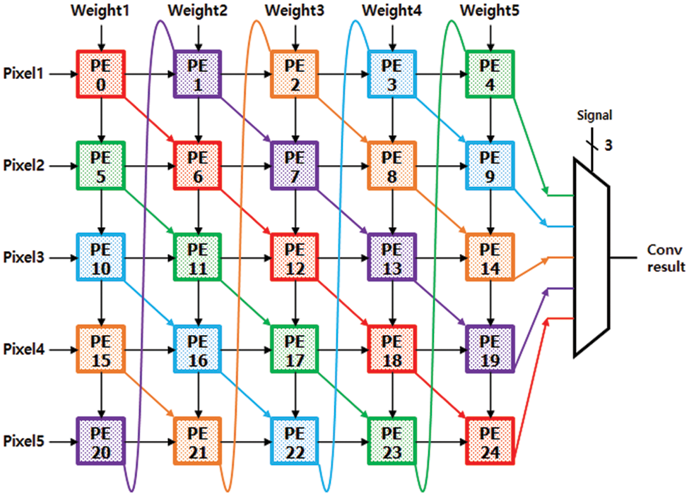
Figure 3: 5 × 5 diagonal cyclic array architecture
2.2 Loading Input Buffers and FIFOs
The host CPU loads Image data and weight parameters to the external DRAM to start a new inference process. The DRAM also stores Feature MAP (FMAP) data and configuration parameters for each layer of the target AI network. In order to prevent stalls in pipeline cycles while loading a burst of data from DRAM to DCA, a common approach is to first store the loaded data in the global input buffer. This data is then transmitted to the weight memories within the DCA and the registers in the PCP block.
Each data-recycle FIFO consists of a register and two FIFO, keeping the data from the global buffer. In the DCA, each of the four columns of sub-arrays has a data-recycle FIFO which is shared by the eight rows of sub-arrays in each column.
2.3 Iteration of DCA for Input Channels
The four columns of the example DCA take four Input Channel data simultaneously from the data-recycle FIFOs, while the eight individual rows of the DCA produce eight FMAP data by sharing the four Input Channel data. DCA then accumulates the partial output FMAP data for each output channel in on-chip memory Conv-mem. DCA iterates the above accumulation process by taking the next four input channels until it finishes entire input channels are taken for the current layer. For this paper’s running example CNN, YOLOv2-Tiny, the first layer has only three channels, while other layers grow up to 1024 channels. In this example, CNN DCA needs only 1 iteration to finish the input channel processing, while other layers require up to 256 iterations.
2.4 Iteration of DCA for Output Channels
Once the input channel iteration is finished for the target output channel in the current layer, the convolution result accumulated in the corresponding address of Conv-mem is passed to the PCP block. PCP block conducts pooling, batch normalization, and activation functions, then stores the results in the on-chip output memory. Since the example of DCA consists of eight rows, it concurrently accumulates eight partial output channel data in Conv-mem, followed by eight concurrent PCP results. The eight PCP results are temporarily stored in the on-chip output memory and then moved to DRAM through the AXI bus. For each layer, if the number of output channels is greater than the DCA’s concurrent output channels (eight in this example), DCA conducts iterations of the above process, including the PCP block, until the entire output channels are finished.
2.5 Iteration of DCA for Input Image Slices
For the above DCA process with input and output channel iterations, Conv-mem tends to increase rapidly as the input image size grows. This is attributed to the nature of Conv-mem that keeps the output FMAP results for all input channels iteratively. To limit the size of on-chip Conv-mem and input buffer to an acceptable range for compact and low-power SoC, we introduce a notion of slice–segmenting the input image to a set of slices of size HS × WS pixels.
3 Operation of the Proposed Architecture
This section describes the proposed accelerator architecture in detail and demonstrates its advantages. Since the primary goal of this study is to reduce the repetition of data loading from DRAM and therefore increase the throughput of data processing, a group of novel ideas, DCA Data recycling FIFO, and post-convolution processes integrated to satisfy this goal in Fig. 4 we can see the block diagram of the proposed accelerator.
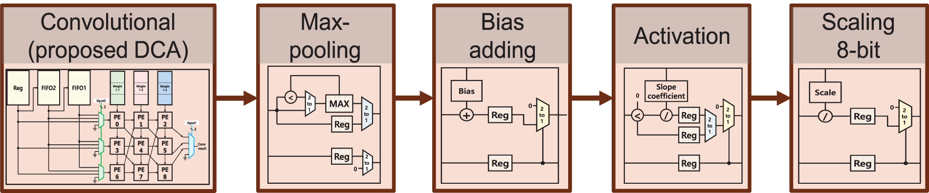
Figure 4: The proposed accelerator bock diagram
3.1 Operation of Diagonal Cyclic Array
For fast Convolution operation, this paper introduces a novel structure of PE array called Diagonal Cyclic Array (DCA), which propagates the convolution results through the diagonal direction in a cyclic fashion. This section describes the structure and operation of the DCA using the above example DCA implementation for the YOLOv2-Tiny model. Fig. 5 illustrates the structure of one sub-array of DCA, which consists of 3 × 3 PEs to calculate one kernel, while Fig. 6 gives the detailed internal structure of one PE. In the kernel-level sub-array, the input feature map or image data is propagated through the horizontal direction of each row.
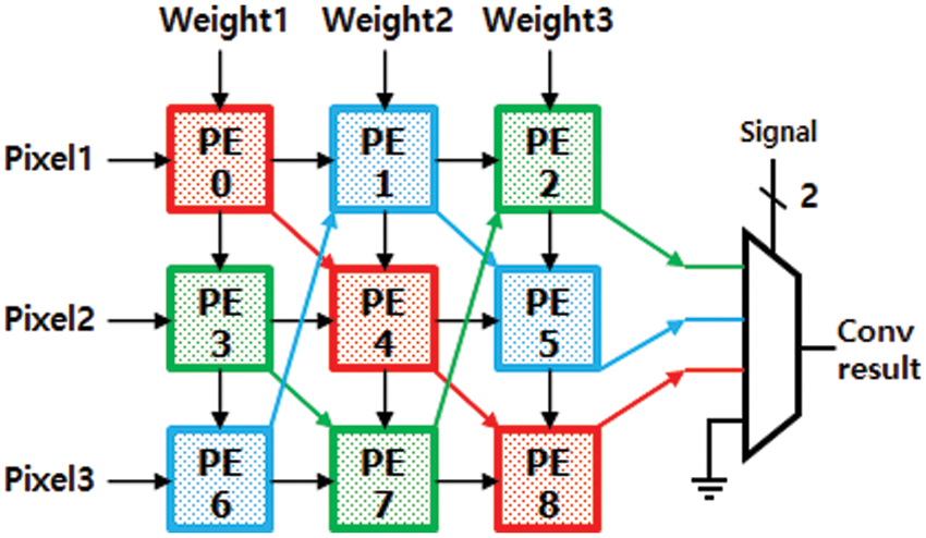
Figure 5: 3 × 3 diagonal cyclic array architecture
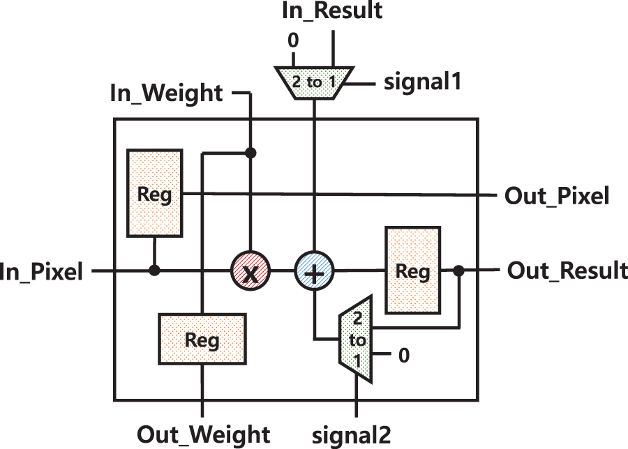
Figure 6: 3 × 3 PE architecture
The weight parameters are passed through the vertical direction of each column of the sub-array. Unlike the conventional PE arrays, DCA has an additional path in the K diagonal directions for a sub-array implementing a kernel of K × K size. For the example of a 3 × 3 kernel, there are three diagonal cyclic paths, which progressively propagate the partial accumulation values of the convolution kernel to the next PE along the three paths until 9 MAC operations for the 3 × 3 convolution kernel are completed. Each of the three diagonal cyclic paths is denoted by three PE boxes with the same colour in Fig. 3. For example, a blue path is denoted by three blue PEs connected by blue arrows. Each PE of each path computes three MACs and propagates the result to the next PE, while the final PE of the path sends the final 3 × 3 kernel result to Conv-mem. For the red path, for example, PE0 multiplies three input image data with three weight parameters, accumulates the three MAC results, and propagates it to PE4 in the red diagonal path. PE4 then accumulates the received value into its 3 MAC results. Finally, PE8 gets the result from PE4 and accumulates it into its own three MAC results, completing 3 × 3 kernel computation and storing it at Conv-mem. All the PEs in the sub-array, upon completion of the three MACs, immediately receive the next sequence of 3 input data and corresponding weights and starts the MACs for the next kernel computation. The controller of DCA reads data from the slice in the following order. Its read window for 3 × 3 FMAP data starts from the top left corner of the slice and moves down to the bottom, then the window shifts to the right by 1 pixel and then moves down. The above read cycles are repeated until the read pointer reaches the bottom right corner of the slice.
Fig. 7a illustrates an example slice of FMAP of size 6 × 6 using a 3 × 3 kernel. Fig. 7b shows the sequences of MACs calculated by the 9 PEs in the example sub-array of Fig. 5. As depicted in Fig. 5b, all PEs operate in a pipelined manner and thus continuously compute MACs for the next kernel without waiting for the completion of the current kernel. In this example sub-array, up to 7 kernel convolutions are performed simultaneously from conv1 to conv8 in Fig. 7b.
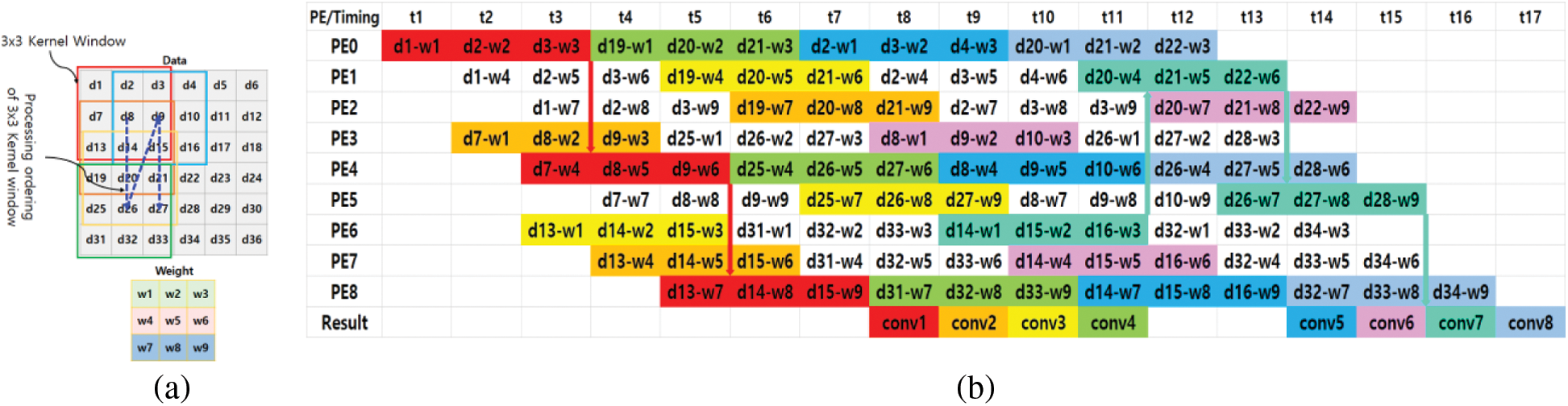
Figure 7: 3 × 3 (a) example slice of input FMAP and a 3 × 3 kernel, (b) timing table of PE’s data input during DCA convolution
3.2 Operation of Data-Recycle FIFOs
Fig. 8 illustrates the proposed input buffer and data-recycle FIFOs connected to the sub-array of the 3 × 3 kernel. The proposed input FIFOs substantially reduce repeated loading of the same data from DRAM, which incurs excessive time and power consumption in conventional architectures. When convolution of one column is performed, since data transmitted in the vertical and horizontal directions are used in multiple PEs, there is no need for duplicate input of the input image. However, for the next column, the same data must be loaded from DRAM up to 3 times because the previously used two lines must be reused. This study proposes a memory structure that enables the reuse of a single value multiple times, thus preventing the issue. The register takes input image or FMAP data from the global input buffer in Fig. 1. The global input buffer receives a burst of input data from DRAM via the AXI bus and forwards it to the register, which also delivers the data to FIFO2. FIFO2 also passes its data to FIFO1. The depth of the FIFOs is configured to the column size of the input slice FMAP. For example, the FIFO depth is set to 6 for the example FMAP size 6 × 6 for the case of Fig. 8.

Figure 8: Input FIFOs and weight buffer for a (3 × 3) sub-array
Fig. 9 illustrates the operation of data-recycle FIFOs for the example sub-array of a (3 × 3) kernel in Fig. 7a. When a predefined amount of data is stored in FIFO1 and FIFO2, all sub-arrays of DCA start their convolution computations. To continuously feed a sequence of input data to the first column of the sub-array, the three data from the register, FIFO2, and FIFO1, respectively, are also connected to the neighbouring FIFOs, not only feeding the PEs of the first column. Steps 1 through 6 in Fig. 9 illustrate how data-recycle FIFOs provide the first 3 × 3 input data (highlighted by a red box in Fig. 7a) to the sub-array. Each step shows how the next three input data and three weights are simultaneously fed to the first column of the sub-array. The red arrows in Fig. 9 show the forwarding paths from register to FIFO2 and then to FIFO1 in a way that maximizes data recycling. The dotted boxes in Fig. 9 indicate the current read pointers that feed three data to the first column of the sub-array: PE0, PE3, and PE6 in this example. The weights from the weight memory are also continuously fed to the first row: PE0, PE1, and PE2 in steps 1 through 6. Using the input data and weights fed by the data-recycle FIFOs and weight memory, the MAC operations conducted by 3 × 3 PEs are illustrated in Fig. 9 along the cycle time. Initially, it takes a latency of 7 cycles after the first data is fed to PE0 for the first convolution to complete. The following convolution results are continuously completed without additional latency. The latency can occur only when the (3 × 3) kernels are completed with the first three columns of the input data slice, and the next three columns are fed. For the small slice example (a slice of 6 × 6 pixels) in Fig. 7a, the sub-array incurs a latency of two cycles when it starts the kernel computation for the next three columns indicated by the blue box; See the two empty results on the bottom row of in Fig. 7b. However, for a larger slice size, the additional latency becomes negligible in overall computation time.
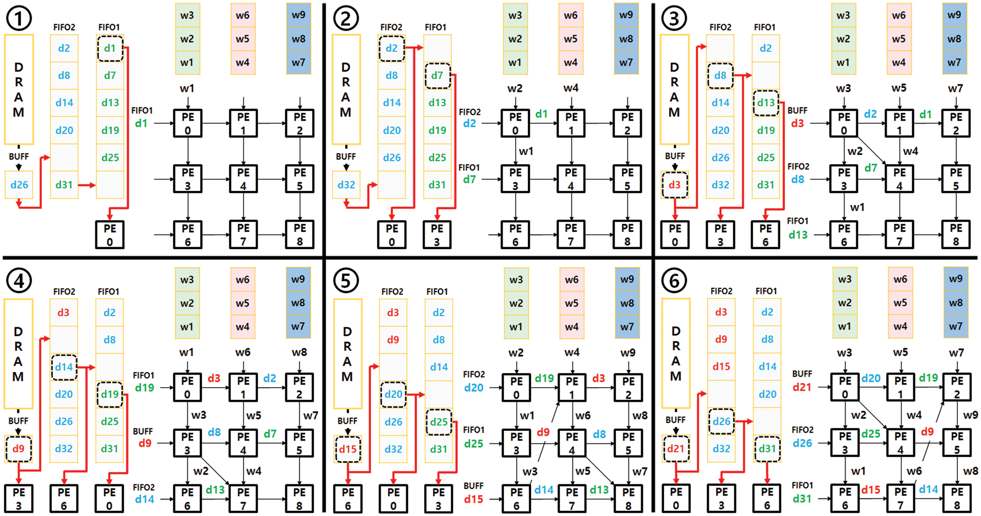
Figure 9: Data-recycle FIFOs and input data flow for the sub-array of 3 × 3 kernel
Eq. (1) calculates the computation latency (in terms of the number of cycles) incurred when the data column changes in a slice, while Eq. (2) calculates the computation latency of the convolution for one slice after the entire data of the slice is fed to the DCA. In Eq. (2),
Fig. 10 compares the number of repeated data loadings for each pixel for GPU-based accelerators and this work. In conventional accelerators based on GPUs or CPUs, to compute convolution, each pixel data in an input slice should be repeatedly reloaded nine times for the case of using a 3 × 3 kernel, as expressed by Eq. (6), which is illustrated in the left image of Fig. 10. However, in the proposed DCA, as defined by Eq. (4), it can reduce data reloading time by up to nearly nine times.
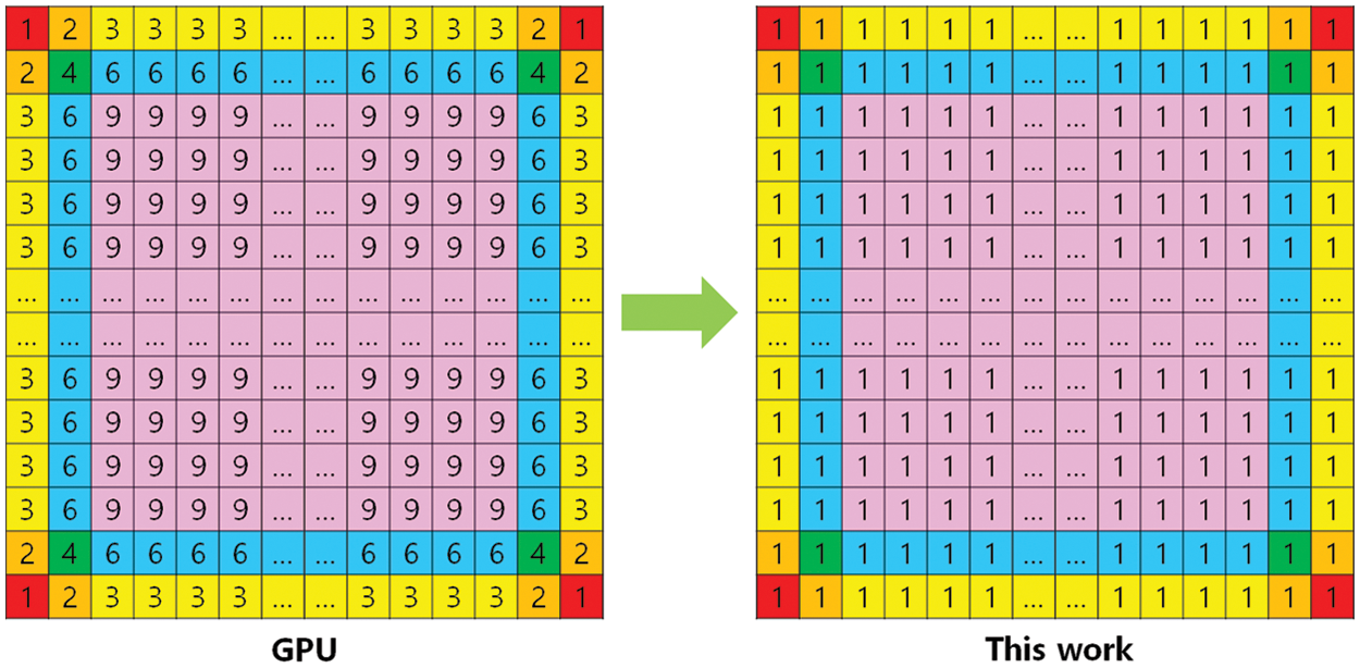
Figure 10: Comparison of repeated data loadings for each pixel for GPU-based accelerators and this work
Fig. 11 compares the number of data load cycles incurred by the proposed work with the conventional implementations based on CPU and GPU, respectively. The proposed work is about eight times more efficient than the GPU-based implementation, which repeatedly reads all the FMAP data needed for convolution calculations. Furthermore, it is about 56 times more efficient than the CPU-based implementation that frequently loads data again from DRAM for every MAC operation.
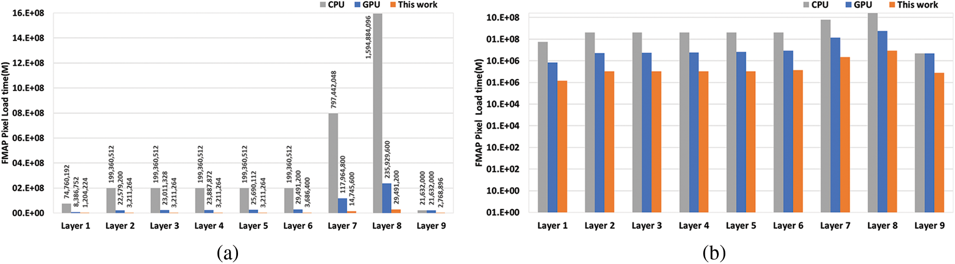
Figure 11: Comparison of the number of data load times from DRAM: (a) Linear scale plot, (b) log scale plot
Through the DCA structure, it was confirmed that the slice size of FMAP determines the convolution latency. However, since one set of DCA structures can calculate one FMAP, it takes a lot of time to calculate all convolutions. To compensate for this, several DCAs implemented in parallel to calculate various channels simultaneously. One approach to increasing the number of parallel input channels is to add the DCAs to the column path. To increase the parallel output channel, again DCAs were added, but in this case, to row way. The example DCA showed in Fig. 1 consists of 8 Rows × 4 Columns which give 32 sub-arrays leading to 288 PEs. To accumulate the convolution results of sub-arrays in the same row, we added an adder to each sub-array which is chained through all sub-arrays in the same row. The accumulated data from these adders in each row is stored in Conv-mem. The output of Conv-mem is passed to the Integrated PCP block, which processes the data concurrently in each row.
3.4 Integrated Post-Convolution Process
To reduce the number of memory accesses for pooling, batch normalization, and activation functions and to reduce overall latency, the PCP block is integrated into a pipelined circuit. Fig. 12 illustrates the pipeline circuit. In conventional architectures, pooling is performed after batch normalization and activation function, which incurs problems of unnecessarily high computation overhead and power consumption. To prevent this problem, we change the operation order. Our architecture conducts first pooling followed by Batch Normalization and Activation functions, significantly reducing computation overhead because the pooling reduces the feature map by four times. We implement a 2 × 2 Max Pooling circuit with one Max register. Max register takes the first data and then compares this data with the following data one by one. If the following data is bigger than the previous data, the next data replaces the maximum register’s value. The pooling stage is bypassed for the layers that do not need pooling. For the layers that do not need pooling, the pooling stage is bypassed. Leaky ReLU is an activation function modified from ReLU by adding a small slope coefficient for the negative values. While YOLOv2 tiny model commonly uses 0.1 for the slope coefficient, the proposed accelerator employs a variable slope coefficient that can be configured to facilitate improving the accuracy performance. The proposed CNN accelerator applies quantization to weight parameters and FMAP data. For the example YOLOv2-tiny model, we used 8-bit quantization.
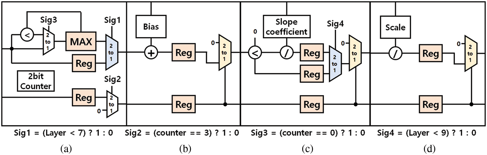
Figure 12: Pipeline architecture, (a) max pooling (b), bias addition (c), activation function, and (d) scale function
The quantization requires a scaling process to recover the original range of the floating-point values. After the activation function, we scale down the output FMAP data by dividing the values by the scale factor in each layer. In most CNN models, padding is added around the input FMAP to calculate convolutions accurately, even at the edges around the FMAP. To reduce on-chip memory size, our padding controller inserts a 0 value instead of reading it from the memory when padding is needed.
The 32 sub-arrays of DCA of the example accelerator implement a small array of 8 rows × 4 columns, which can compute eight output channels with four input channels at the same time. This can cover only a small portion compared to the convolution calculations needed to complete the target CNN model. Therefore, DCA iterates over the input channels that exceed four channels and repeats over the output channels that exceed eight channels in each layer. In each iteration, the temporary convolution results are accumulated into Conv-Mem. The convolution process of each consists of three hierarchical iterations, iterations for covering all input channels, iterations for scanning the entire FMAP by shifting the slice, and iterations for covering all output channels.
Fig. 13 illustrates the three hierarchical iterations assuming that the current layer has 16 input channels, an FMAP size of 54 × 52, and 32 output channels. Since the example DCA has four columns, it can cover the 16 input channels in 4 input iterations. Assuming the slice size of 26 × 26, it can cover the FMAP in four iterations. Since the DCA has eight rows, it can cover the 32 output channels in four output iterations, and to cover the FMAP data in the slice, it requires four slice iterations. The iteration parameters are programmable depending on the target CNN model. Among the three levels of hierarchical iterations, the number of input iterations is calculated by Eq. (7).

Figure 13: Scanning the input FMAP by shifting the slice vertically over the input FMAP
For the example accelerator of Fig. 1, which has four concurrent input channels, each group of four input channels concurrently produces their partial FMAPs in each iteration. The input iterations continue until the current CNN layer input channels are covered. Fig. 14 shows the on-chip memory occupancy ratio for each block in the accelerator example of Fig. 1. Conv-mem occupies 75% of the total on-chip memory, as shown in Fig. 14. The size of the Conv-Mem increases as the size of FMAP of the layer increases. However, since the size of the FMAP usually becomes smaller for deeper layers, Conv-Mem can be well-spent if too large Conv-Mem is chosen. In order to decrease the size of Conv-Mem, this paper proposes dividing the input image into smaller slices, performing iterative convolutions on each slice, and generating a slice of the output feature map for each output channel. Once all slice iterations are finished, the slice is vertically moved to the next slice in the input FMAP; See Fig. 15.
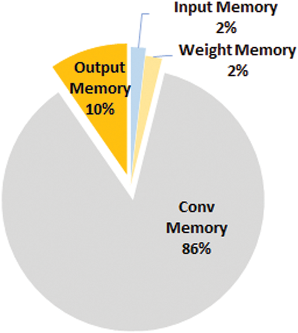
Figure 14: On-chip memory occupancy ratio
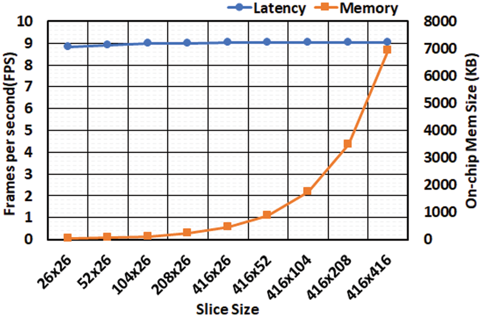
Figure 15: On-chip memory occupancy ratio
When the slice moves, there is overlapped data between the previous slice and the current slice, which is read multiple times (reading two times on the edges and four times on the corners) speed in frames per second (FPS). However, Fig. 16 shows the changes in the required on-chip memory size and the inference speed over increasing slice size. For example, if we compared the slice of 26 × 26 against the slice of 416 × 416, the on-chip memory is substantially reduced by 32 times while the inference speed is marginally dropped only by 3%. This analysis leads to an important design decision. The smallest slice (e.g., 26 × 26) is the best choice since the smallest slice incurs almost no loss in the inference speed while providing minimum on-chip memory. Eq. (8) denotes the number of slice iterations S required to cover the entire input FMAP.
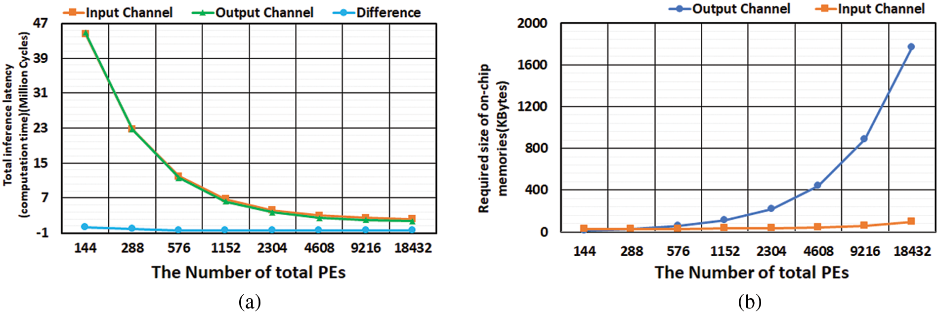
Figure 16: The impact of increasing the number of PEs on (a) inference latency and (b) required memory size
The 3rd level of the hierarchical iterations and the output iteration is conducted as follows. The input and slice iterations are conducted over eight concurrent output channels, for example, DCA of Fig. 1. After the input and slice iterations are completed for the current eight output channels, the DCA starts new input and slice iterations for the following eight output channels. The output iterations continue the above process until all output channels are covered. Eq. (9) shows how to calculate the number of output iterations.
The proposed DCA can configure the number of iterations in the hierarchical iterations for a different number of input and output channels and varying FMAP sizes in each layer. To reduce the on-chip memory size of the accelerator of Fig. 1, we chose a slice of 26-26, which incurs the minimum cost at little loss of inference speed based on the analysis of Fig. 16a. Table 2 summarizes the number of hierarchical iterations in each layer of YOLOv2-tiny implemented using the accelerator of Fig. 1. Each column of Table 2 indicates the size of input FMAP data, the total number of input and output channels, the input iterations, slice iterations, output iterations followed by the total number of all iterations in each layer. The slice iteration affects the size of on-chip memory and the inference latency. Reducing the number of iterations is necessary to decrease the inference latency. There are two ways to minimize the total number of iterations; the first is to increase the number of parallel input channels to reduce the input iterations. However, increasing the parallel data load from the input memory leads to higher hardware costs.

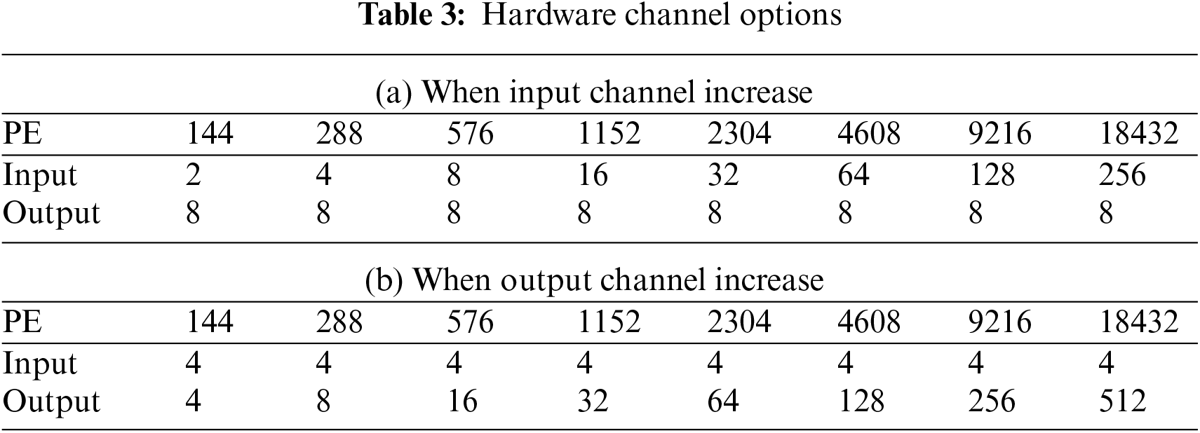
The second method is to increase the number of parallel output channels to reduce output iterations. However, this method dramatically increases the size of on-chip memories, specifically, Conv-Mem and output buff. Figs. 16a and 16b show the changes in inference latency and required memory size when growing the number of PEs by two approaches: first, by increasing the number of parallel input channels and second, by increasing the number of parallel output channels. Table 3(a) shows the first approach with eight parallel output channels, while Table 3(b) shows the second approach with four parallel output channels. For both approaches, the inference latency decreases similarly in Fig. 16b. In contrast, the required memory increase rate drastically differs between the two approaches. Therefore, Figs. 16a and 16b reveal that the better design decision is to increase the number of parallel input channels rather than output channels to reduce the inference latency.
In this work, we propose a network optimization method which includes modifying the DNN model architecture and a straightforward, simple, yet post-training quantization methodology for the object detection tasks. The proposed methodology can be applied to various CNN models. In the network optimization, we use batch normalization folding to reduce computation complexity, as shown in Eq. (10). In Eq. (10),
While the training process determines these parameters, they are constants in the inference process [26,29]. Therefore, we can fold the batch normalization parameters (
To further optimize the model, we merge convolutional and batch normalization processes in one process described by Eqs. (12) and (13).
The proposed quantization method is applied to the model obtained by the folding process, and the following steps describe the quantization method.
We analyze the max/min values of each layer’s output features to determine the ranges and the required bit-width of feature values. Then we determine the scaling factors to represent the output feature values. For the target model, YOLOv2-Tiny, we selected a 750-input image from the Visual Object Classes (VOC) 2007 dataset as a calibration dataset.
For the range determined above, we remove outlier weights that are out of the range. Then, we adjust the range to keep the Mean Squared Error (MSE) for the weights obtained after the outlier removal under a specified limit. We observed that applying this outlier-removing step before the quantization process could keep the performance degradation below 1% in the case of 8-bit full integer quantization.
5.3 Model Parameters Quantization
In this step, we convert the weights and biases of the model from a 32-bit floating-point to an 8-bit integer and calculate the corresponding scaling factors. Eqs. (14) and (15) determine the scaling factor and quantized parameters, respectively, where n represents the number of bits,
Eq. (16) and Fig. 17 show how quantized integer feature data are determined for each layer. Although the activation function (Leak ReLU for YOLOv2) and the scaling function (Divider) produce fractional numbers, the fraction portion is truncated to make them integer values for simplicity with little or no sacrifice of the accuracy. This step completes the quantization process of all feature data and parameters, ensuring the resulting datapath hardware only needs integer operators.

Figure 17: Overview of full 8-bit integer quantization: (a) layers 1∼6; (b) layers 7 and 8; (c) layer 9
To demonstrate the advantages of the proposed accelerator, we implemented the proposed accelerator of Fig. 1 using the Xilinx Zynq ZCU102 Ultrascale+ FPGA platform. We implemented the proposed accelerator based on the example DCA described in Fig. 1, consisting of 288 PEs. We designed the controller for the accelerator using a compact micro-code execution unit, which offers high programmability at a minuscule-hardware cost compared with conventional CPU cores. For the proposed CNN accelerator, we configured the implemented accelerator for the YOLOv2-tiny model that was trained using the PASCAL VOC dataset. Its weight parameters and output FMAP (activation data) are quantized into 16-bit and 8-bit integers. This model’s accuracy (mAP 0.5) evaluated in the software framework is 57.92% and 56.42%. It was confirmed that the FPGA implementation shows the same accuracy as the software framework in both cases. Fig. 18 shows the FPGA platform, where the FPGA board receives image data from a Host PC, computes object detection CNN and sends the detection result back to the Host PC. The FPGA implementation occupies 34336 LUTs, 58 kB BRAMs, and 576 DSPs. The inference computation time for one image is 137.9 ms at an FPGA clock frequency of 200 MHz, corresponding to 7.3 frames per second (FPS). Table 4 compares our FPGA implementation result with prior works [8,31–33], which implement the same CNN model YOLOv2-Tiny. The most prominent advantage of our work is that it requires minimal on-chip memory. The on-chip SRAM (BRAM) used by our FPGA implementation are 4.4, 28.2, 37.2, and 39.8 times smaller than the BRAM required by the work of [8,31–33], respectively. In addition, the FPGA logic size in terms of LUT count used by our implementation is 2.45, 3.3, 2.8, and 2.5 times smaller than the works of [8,31–33], respectively.

Figure 18: FPGA board setup and inference output of (a) VOC 2007 dataset and (b) mask/no mask dataset

After verifying the proposed accelerator design using FPGA, we implemented it in an SoC silicon using the Taiwan Semiconductor Manufacturing Company (TSMC) 55 nm Complementary Metal Oxide Semiconductor (CMOS) process. The chip area is

Figure 19: Full chip layout implemented in 55 nm process
This paper proposes a CNN accelerator that employs a novel architecture based on the diagonal cyclic array (DCA), Data Recycle FIFO. An optimization of the neural network was proposed, including modification of network architecture and integer-only quantization method that can quantize all internal computation as well as the parameters in the memory to reduce resource consumption. While most previous quantization methods can handle simpler models like image classification CNNs and not a pure integer, the proposed quantization method can handle more complex models, including object detection CNNs with only integer operations, which facilitate the data manipulation processes with minor performance loss. The proposed architecture can substantially reduce the on-chip memory and minimize the repeated accesses to external DRAM by maximizing data reuse, which can be suitable for real applications such as autonomous vehicles and allowing the implementation of CNN on resource-constrained devices like modern IoT and mobile devices. Our thorough analysis of the accelerator confirmed that increasing its parallel input channels is more effective than increasing the output channels to obtain higher speeds while minimizing the memory overhead. To demonstrate the performance of the proposed accelerator architecture, we implemented an accelerator with a DCA of 288 PEs employing four parallel input channels and eight parallel output channels. We verified the accelerator design using FPGA implementation for both 8-bit and 16-bit versions and then implemented it in an SoC silicon using a CMOS 55 nm process. Comparison with prior works unveiled that the proposed accelerator significantly reduces on-chip memory by 28.2∼39.8 times and FPGA logic size (LUTs) by 3.3∼2.5 times.
Funding Statement: This work was supported by the National Research Foundation of Korea (NRF) grant funded by the Korea government (MSIT) (No. 2022R1A5A8026986) and supported by the Institute of Information & communications Technology Planning & Evaluation (IITP) grant funded by the Korean government (MSIT) (No. 2020-0-01304, Development of Self-learnable Mobile Recursive Neural Network Processor Technology). It was also supported by the MSIT (Ministry of Science and ICT), Korea, under the Grand Information Technology Research Center support program (IITP-2023-2020-0-01462) supervised by the IITP (Institute for Information & communications Technology Planning & Evaluation) and supported by the National Research Foundation of Korea (NRF) grant funded by the Korea government (MSIT) (No. 2021R1F1A1061314). In addition, this work was conducted during the research year of Chungbuk National University in 2020.
Conflicts of Interest: The authors declare that they have no conflicts of interest to report regarding the present study.
References
1. J. Redmon, S. Divvala, R. Girshick and A. Farhadi, “You only look once: Unified, real-time object detection,” in Proc. of IEEE Conf. on Computer Vision and Pattern Recognition (CVPR), Las Vegas, Nevada, USA, pp. 779–788, 2016. [Google Scholar]
2. Y. C. Lu, C. W. Chen, C. C. Pu, Y. T. Lin, J. K. Jhan et al., “An 176.3 GOPs object detection CNN accelerator emulated in a 28 nm CMOS technology,” in 2021 IEEE 3rd Int. Conf. on Artificial Intelligence Circuits and Systems (AICAS), Washington, DC, USA, IEEE, pp. 1–4, 2021. [Google Scholar]
3. C. Zhang, G. Sun, Z. Fang, P. Zhou, P. Pan et al., “Caffeine: Toward uniformed representation and acceleration for deep convolutional neural networks,” IEEE Transactions on Computer-Aided Design of Integrated Circuits and Systems, vol. 38, no. 11, pp. 2072–2085, 2018. [Google Scholar]
4. J. Li, K. F. Un, W. H. Yu, P. I. Mak and R. P. Martins, “An FPGA-based energy-efficient reconfigurable convolutional neural network accelerator for object recognition applications,” IEEE Transactions on Circuits and Systems II: Express Briefs, vol. 68, no. 9, pp. 3143–3147, 2021. [Google Scholar]
5. J. Qiu, J. Wang, S. Yao, K. Guo, B. Li et al., “Going deeper with embedded FPGA platform for convolutional neural network,” in Proc. of the 2016 ACM/SIGDA Int. Symp. on Field-Programmable Gate Arrays, Monterey, CA, USA, pp. 26–35, 2016. [Google Scholar]
6. J. Kim, J. -K. Kang and Y. Kim, “A resource efficient integer-arithmetic-only FPGA-based CNN accelerator for real-time facial emotion recognition,” IEEE Access, vol. 9, pp. 104367–104381, 2021. [Google Scholar]
7. K. W. Chang and T. S. Chang, “VWA: Hardware efficient vectorwise accelerator for convolutional neural network,” IEEE Transactions on Circuits and Systems I: Regular Papers, vol. 67, no. 1, pp. 145–154, 2020. [Google Scholar]
8. J. Zhang, L. Cheng, C. Li, Y. Li, G. He et al., “A Low-latency FPGA implementation for real-time object detection,” in 2021 IEEE Int. Symp. on Circuits and Systems (ISCAS), Daegu, Korea, pp. 1–5, 2021. [Google Scholar]
9. Y. Yao, Q. Duan, Z. Zhang, J. Gao, J. Wang et al., “A FPGA-based hardware accelerator for multiple convolutional neural networks,” in 2018 14th IEEE Int. Conf. on Solid-State and Integrated Circuit Technology (ICSICT), Qingdao, China, IEEE, pp. 1–3, 2018. [Google Scholar]
10. A. Kyriakos, V. Kitsakis, A. Louropoulos, E. A. Papatheofanous, I. Patronas et al., “High performance accelerator for CNN applications,” in Int. Symp. on Power and Timing Modeling, Optimization and Simulation (PATMOS), Rhodes Island, Greece, IEEE, pp. 135–140, 2019. [Google Scholar]
11. L. Kang, H. Li, X. Li and H. Zheng, “Design of convolution operation accelerator based on FPGA,” in 2020 2nd Int. Conf. on Machine Learning, Big Data and Business Intelligence (MLBDBI), Taiyuan, China, IEEE, pp. 80–84, 2020. [Google Scholar]
12. Y. H. Chen, T. Krishna, J. S. Emer and V. Sze, “Eyeriss: An energy-efficient reconfigurable accelerator for deep convolutional neural networks,” IEEE Journal of Solid-State Circuits, vol. 52, no. 1, pp. 127–138, 2016. [Google Scholar]
13. F. Indirli, A. Erdem and C. Silvano, “A Tile-based fused-layer CNN accelerator for FPGAs,” in 2020 27th IEEE Int. Conf. on Electronics, Circuits and Systems (ICECS), Glasgow, Scotland, IEEE, pp. 1–4, 2020. [Google Scholar]
14. Y. Parmar and K. Sridharan, “A resource-efficient multiplierless systolic array architecture for convolutions in deep networks,” IEEE Transactions on Circuits and Systems II: Express Briefs, vol. 67, no. 2, pp. 370–374, 2019. [Google Scholar]
15. Y. Huan, J. Xu, L. Zheng, H. Tenhunen and Z. Zou, “A 3D tiled low power accelerator for convolutional neural network,” in 2018 IEEE Int. Symp. on Circuits and Systems (ISCAS), Florence, Italy, IEEE, pp. 1–5, 2018. [Google Scholar]
16. F. Tu, S. Yin, P. Ouyang, S. Tang, L. Liu et al., “Deep convolutional neural network architecture with reconfigurable computation patterns,” IEEE Transactions on Very Large Scale Integration (VLSI) Systems, vol. 25, no. 8, pp. 2220–2233, 2017. [Google Scholar]
17. C. N. Liu, Y. A. Lai, C. H. Kuo and S. A. Zhan, “Design of 2D systolic array accelerator for quantized convolutional neural networks,” in 2021 Int. Symp. on VLSI Design, Automation and Test (VLSI-DAT), Hsinchu, Taiwan, IEEE, pp. 1–4, 2021. [Google Scholar]
18. J. Yang, W. Fu, X. Cheng, X. Ye, P. Dai et al., “S2 engine: A novel systolic architecture for sparse convolutional neural networks,” IEEE Transactions on Computers, vol. 71, no. 6, pp. 1440–1452, 2021. [Google Scholar]
19. Y. Li, S. Lu, J. Luo, W. Pang and H. Liu, “High-performance convolutional neural network accelerator based on systolic arrays and quantization,” in 2019 IEEE 4th Int. Conf. on Signal and Image Processing (ICSIP), Wuxi, China, IEEE, pp. 335–339, 2019. [Google Scholar]
20. W. Liu, J. Lin and Z. Wang, “USCA: A unified systolic convolution array architecture for accelerating sparse neural network,” in 2019 IEEE Int. Symp. on Circuits and Systems (ISCAS), Sapporo, Hokkaido, Japan, IEEE, pp. 1–5, 2019. [Google Scholar]
21. Y. Zeng, H. Sun, J. Katto and Y. Fan, “Accelerating convolutional neural network inference based on a reconfigurable sliced systolic array,” in 2021 IEEE Int. Symp. on Circuits and Systems (ISCAS), Daegu, Korea, IEEE, pp. 1–5, 2021. [Google Scholar]
22. H. Kim, S. Lee, J. Choi and J. H. Ahn, “Row-streaming dataflow using a chaining buffer and systolic array+ structure,” IEEE Computer Architecture Letters, vol. 20, no. 1, pp. 34–37, 2021. [Google Scholar]
23. A. Ibrahim, F. Gebali, Y. Bouteraa, U. Tariq, T. Ahanger et al., “Compact bit-parallel systolic multiplier over GF(2m),” IEEE Canadian Journal of Electrical and Computer Engineering, vol. 44, no. 2, pp. 199–205, 2021. [Google Scholar]
24. U. S. Solangi, M. Ibtesam, M. A. Ansari, J. Kim and S. Park, “Test architecture for systolic array of edge-based ai accelerator,” IEEE Access, vol. 9, pp. 96700–96710, 2021. [Google Scholar]
25. C. Kim, H. M. Kim, C. -G. Lyuh, Y. C. P. Cho, J. Yang et al., “Implementation of YOLO-v2 image recognition and other testbenches for a CNN accelerator,” in 2019 IEEE 9th Int. Conf. on Consumer Electronics (ICCE-Berlin), Berlin, Germany, IEEE, pp. 242–247, 2019. [Google Scholar]
26. Z. Xia, J. Chen, Q. Huang, J. Luo and J. Hu, “Neural synaptic plasticity-inspired computing: A high computing efficient deep convolutional neural network accelerator,” IEEE Transactions on Circuits and Systems I: Regular Papers, vol. 68, no. 2, pp. 728–740, 2020. [Google Scholar]
27. Y. Yu, C. Wu, T. Zhao, K. Wang and L. He, “OPU: An FPGA-based overlay processor for convolutional neural networks,” IEEE Transactions on Very Large Scale Integration (VLSI) Systems, vol. 28, no. 1, pp. 35–47, 2019. [Google Scholar]
28. J. Xu, Y. Huan, B. Huang, H. Chu, Y. Jin et al., “A memory-efficient CNN accelerator using segmented logarithmic quantization and multi-cluster architecture,” IEEE Transactions on Circuits and Systems II: Express Briefs, vol. 68, no. 6, pp. 2142–2146, 2020. [Google Scholar]
29. D. Pestana, P. R. Miranda, J. D. Lopes, R. P. Duarte, M. P. Véstias et al., “A full featured configurable accelerator for object detection with YOLO,” IEEE Access, vol. 9, pp. 75864–75877, 2021. [Google Scholar]
30. S. Ioffe and C. Szegedy, “Batch normalization: Accelerating deep network training by reducing internal covariate shift,” in Int. Conf. on Machine Learning, Lille, France, PMLR, vol. 37, pp. 448–456, 2015. [Google Scholar]
31. D. T. Nguyen, T. N. Nguyen, H. Kim and H. J. Lee, “A high-throughput and power-efficient FPGA implementation of YOLO CNN for object detection,” IEEE Transactions on Very Large Scale Integration (VLSI) Systems, vol. 27, no. 8, pp. 1861–1873, 2019. [Google Scholar]
32. S. Zhang, J. Cao, Q. Zhang, Q. Zhang, Y. Zhang et al., “An FPGA-based reconfigurable CNN accelerator for YOLO,” in 2020 IEEE 3rd Int. Conf. on Electronics Technology (ICET), Chengdu, China, IEEE, pp. 74–78, 2020. [Google Scholar]
33. Y. J. Wai1, Z. B. M. Yussof, S. I. B. Salim and L. K. Chuan, “Fixed point implementation of tiny-YOLO-v2 using opencl on FPGA,” International Journal of Advanced Computer Science and Applications, vol. 9, no. 10, pp. 506–512, 2018. [Google Scholar]
Cite This Article
 Copyright © 2023 The Author(s). Published by Tech Science Press.
This work is licensed under a Creative Commons Attribution 4.0 International License , which permits unrestricted use, distribution, and reproduction in any medium, provided the original work is properly cited.
 Downloads
 Citation Tools