
 Submit a Paper
 Propose a Special lssue
 Open Access
ARTICLE

Boosted Stacking Ensemble Machine Learning Method for Wafer Map Pattern Classification
1 Department of Convergence and Fusion System Engineering, Kyungpook National University, Sangju, 37224, Korea
2 Department of Mathematics, Natural and Economic Sciences, Ulm University of Applied Sciences, Ulm, 89075, Germany
* Corresponding Author: Dongjun Suh. Email:
Computers, Materials & Continua 2023, 74(2), 2945-2966. https://doi.org/10.32604/cmc.2023.033417
Received 16 June 2022; Accepted 02 August 2022; Issue published 31 October 2022
 View Full Text
 Download PDF
Abstract
Recently, machine learning-based technologies have been developed to automate the classification of wafer map defect patterns during semiconductor manufacturing. The existing approaches used in the wafer map pattern classification include directly learning the image through a convolution neural network and applying the ensemble method after extracting image features. This study aims to classify wafer map defects more effectively and derive robust algorithms even for datasets with insufficient defect patterns. First, the number of defects during the actual process may be limited. Therefore, insufficient data are generated using convolutional auto-encoder (CAE), and the expanded data are verified using the evaluation technique of structural similarity index measure (SSIM). After extracting handcrafted features, a boosted stacking ensemble model that integrates the four base-level classifiers with the extreme gradient boosting classifier as a meta-level classifier is designed and built for training the model based on the expanded data for final prediction. Since the proposed algorithm shows better performance than those of existing ensemble classifiers even for insufficient defect patterns, the results of this study will contribute to improving the product quality and yield of the actual semiconductor manufacturing process.Keywords
A wafer is a basic unit created to evaluate electrical properties during semiconductor manufacturing [1], where wafer map fabrication is used to visualize the location of defects on the wafer map. Defective IC chips usually show defect patterns on the wafer map. These defect patterns include useful information about the semiconductor manufacturing process. Thus, wafer map defect pattern classification is essential to investigate the root cause of such defects occurring in the semiconductor manufacturing process. For example, physical etching frequently produces edge-ring patterns, while chemical etching often produces circle and scratch patterns. Therefore, accurate identification and classification of these defect patterns increases the chances of fixing the root cause of the main problem [2].
In the actual semiconductor manufacturing process, the occurrence of defects is very rare. In general, there are very few cases with detectable defect patterns when collecting manufacturing process data, and most of the data are in a normal state. Since it is necessary to classify data with a small defect pattern by learning the imbalanced dataset, the classification accuracy is very poor and time consuming [3]. Furthermore, pattern classification for the collected wafer map data relies on visual inspection by skilled engineers. Engineers randomly select samples from entire wafers and use high-resolution microscopy to analyze defects, which is a time-consuming and inconsistent process [4]. In order to save time and money in this process, it is essential to study automated wafer map pattern classification algorithms [5]. A considerable amount of research is underway now on wafer map defect classification using feature extraction algorithms in the semiconductor manufacturing process. Wafer map defect patterns were successfully classified in initial studies by applying only machine learning without applying feature extraction techniques [6]. In addition, research investigating the techniques for extracting features by concentrating on the features of the wafer map has been performed [7–10]. Further, this feature extraction technique was applied to analyze spatial defect patterns using machine learning and automated clustering algorithms [11–13]. In recent studies, defects have been analyzed by directly extracting features from deep learning-based images. There are also many studies that have successfully implemented wafer map defect classification by applying the feature extraction technique followed by an ensemble learning algorithm [14–20].
In order to improve wafer map pattern classification accuracy, this study aims to suggest a Boosted Stacking Ensemble Machine Learning (BSEML) algorithm that applies data augmentation to insufficient defect patterns. With a given training dataset, data augmentation is first performed through CAE-based model learning. Then, features are extracted through handcrafted feature extraction techniques based on features such as density, Radon, and geometry. The extracted feature vectors are combined to construct a BSEML model that performs final prediction. The contributions of this study are listed as follows.
1. The effectiveness of the proposed technique was verified using wafer datasets collected from semiconductor manufacturers.
2. The computational efficiency was increased by extracting the key defect pattern information hidden from the original image using various feature extraction techniques.
3. Data augmentation was performed using a CAE-based model to solve the problem of lack of defect patterns and imbalance, and the accuracy of the proposed model was improved using augmented data.
The rest of this study is structured as follows. Section 2 briefly describes the techniques used in related studies. Section 3 introduces the proposed algorithm. Section 4 describes the data structure and experimental methods. Sections 5 and 6 contain the results of the study and conclusions
In the past few years, there have been many studies that have applied machine learning to wafer map pattern classification. These are largely divided into two types based on the method of extracting the features of the wafer map and classifying the defects. Tab. 1 summarizes literature reported in the related studies.

2.1 Wafer Map Pattern Classification
The first method is to extract hand-made features and build a ready-made classifier. The most commonly used features for feature extraction techniques in this approach include density, geometry, and Radon properties [7]. Such handcrafted feature extraction reduces dimensionality by transforming the wafer map into a vector form. Next, it takes a vector as input and makes predictions in the classification model. This step involves various existing learning algorithms such as support vector machine (SVM), logistic regression (LR), naive Bayes (NB), and K-nearest neighbors (K-NN). The SVM model can be constructed more simply than the existing neural network model, and it is characterized by less overfitting as it has no effect on multi-class data classification and error data [10]. In addition, Baly et al. preprocessed the wafer map through End-of-line (EOL) test before classification using the SVM classifier [6]. The LR model is a widely used classification model, which provides probabilities for classified classes. This is a big advantage over models that can only do final classification [21].
The NB model is based on Bayes’ theorem and learns very quickly compared to existing learning algorithms. In particular, it allows easy and quick prediction in multi-class classification that is probabilistically independent [22]. It has high accuracy as the K-NN model checks and compares all classification system values, and the error data is excluded from the comparison target, thus not affecting the resulting value [23]. Yu et al. maximized classification performance through image denoising with median filter using an algorithm based on a KNN classifier [24]. Studies based on these methods focus on designing model optimizations to enhance the performance of pattern classification. These methods, however, do not overcome the limitations of the models, and some important information from the raw wafer map image might be lost.
The second method is a CNN-based raw image classification method. As shown in Fig. 1, the method aims to detect defects by extracting features from the wafer map based on image data. CNNs are end-to-end models designed to process two or more dimensional arrays as input. The end-to-end model approach is useful as it does not require the development of feature extractors [25]. CNN can directly extract the convolution features and apply them to the wafer map since the wafer map is expressed as a two-dimensional array. Such advantages allow this method to be actively applied to the classification of wafer maps [26–28]. In addition, CNN-based wafer map classification studies using various data processing techniques have been conducted until recently [28–32].

Figure 1: The architecture of convolution neural network approach [25]
2.2 Ensemble Model Learning of Handcrafted Features
The ensemble system is constructed based on principles such as reliability estimation, data fusion, and unbalanced data processing. The performance of an ensemble system depends on the accuracy of individual classifiers and the number of base-level classifiers included [33]. However, it is very difficult to select an appropriate classifier for designing an ensemble system. The ML classifier used in wafer defect classification may be suitable for some defects, but may not be suitable for recognizing all defect classes [34]. The ensemble techniques are used to overcome the limitations of individual classifiers in ML. Learning by assigning specific weights to individual classifiers ensures robustness for all defect classes. The goal of the ensemble classification technique is to integrate the prediction results of various ML models within the given training data and generate the final prediction result with improved accuracy [35]. It also facilitates fast classification through minimal calculations, coupled with handcrafted features that improve defect identification on large-scale wafer data [36].
In recent years, increasing interest in ensemble techniques has led to the emergence of various ensemble-based algorithms such as Voting, Bagging, Boosting, AdaBoost, XGBoost, and Mixture of Experts (MoE) [37]. Accordingly, studies applying the ensemble classification technique to classify wafer map defect patterns have appeared. The voting method first combines different algorithm models.
There are three types of voting methods for deriving the result: the majority, hard, and soft voting methods. Through experimental verification, the soft voting ensemble method has been verified to have the best performance for deriving the final result [17]. The bagging ensemble method allows for redundancy in the data sample and extracts the sample, and then learns by using different sample combinations within the same algorithm, decision tree (DT) or random forest (RF). Subsequently, the average of the results is calculated to obtain the final result. A robust model for various defect patterns has been presented according to the mathematical model of DT, an internal algorithm [18].
This section describes the technique proposed in this study in detail. Fig. 2 shows the process for the proposed technique. The process is as follows. There are cases in which raw wafer image data have a class imbalance or lack defect patterns. Data augmentation using the CAE model is implemented to expand the data by matching the ratio for the overall insufficient pattern. To extract the features of augmented data as much as possible through the ML-based classifier, the amount of computation is reduced by reducing the dimension of the 2D array image to a 1D array while minimizing the loss of feature information due to the lowering of the dimension [38]. By extracting Radon, density, and geometric-based features, the feature vectors are maintained and summed into the BSEML model. Finally, the summed feature vectors are learned by the base-level classifier inside the BSEML model and the final prediction is performed by the meta-level classifier.

Figure 2: The architecture of the proposed method
The feature extraction technique makes a one-dimensional array by reducing the dimension of a two-dimensional array of the wafer map that exists as an image. With the dimension reduction, not only the amount of computation is reduced, but also important feature information is vectorized and converted into a one-dimensional vector [39]. Fig. 3 presents sample wafer maps from each defect pattern type.

Figure 3: Sample images
First, the density-based feature extraction technique is a method of calculating how densely the defects are in the corresponding section of the wafer map [9]. In order to extract the density-based features, each wafer map is divided into 20 parts of the (6, 6) region, and the failure density in each part is calculated. As shown in Fig. 4, the defect density distributions in the respective wafer regions are also different for different defect patterns.
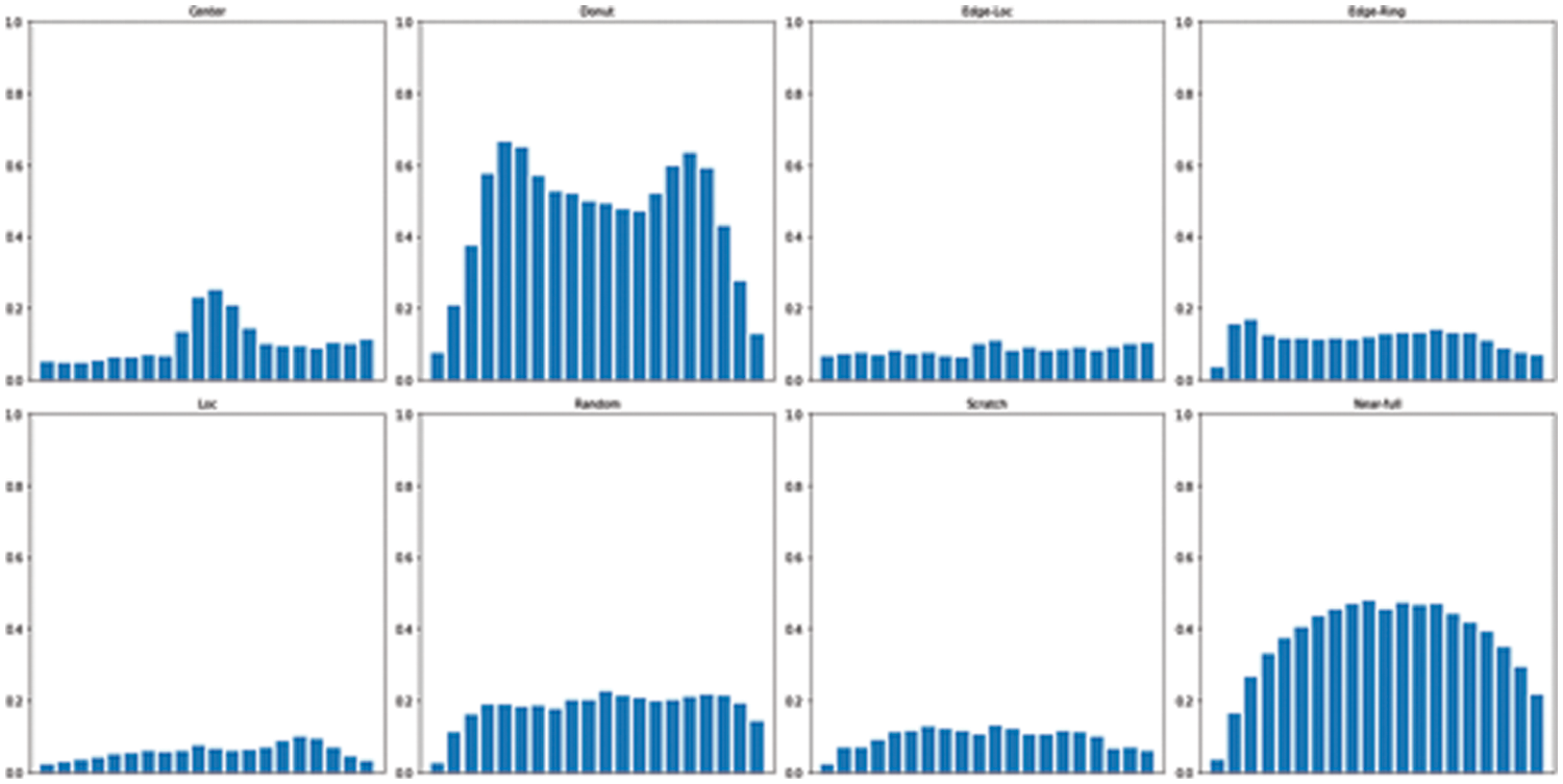
Figure 4: Density-based images
Second, the Radon-based feature extraction technique is a method to generate an image of a two-dimensional representation of a wafer map by Radon transformation based on projection [40]. A projection is constructed by creating a few parallel rays from an object of interest in a 2D image, transferring the object’s integral contrast along with all of the rays to a single pixel in the projection. A Sinogram, which depicts the original image in a linear transform, is a collection of these projections from various angles [8]. The Radon transformation is expressed in Eq. (1).
Here,
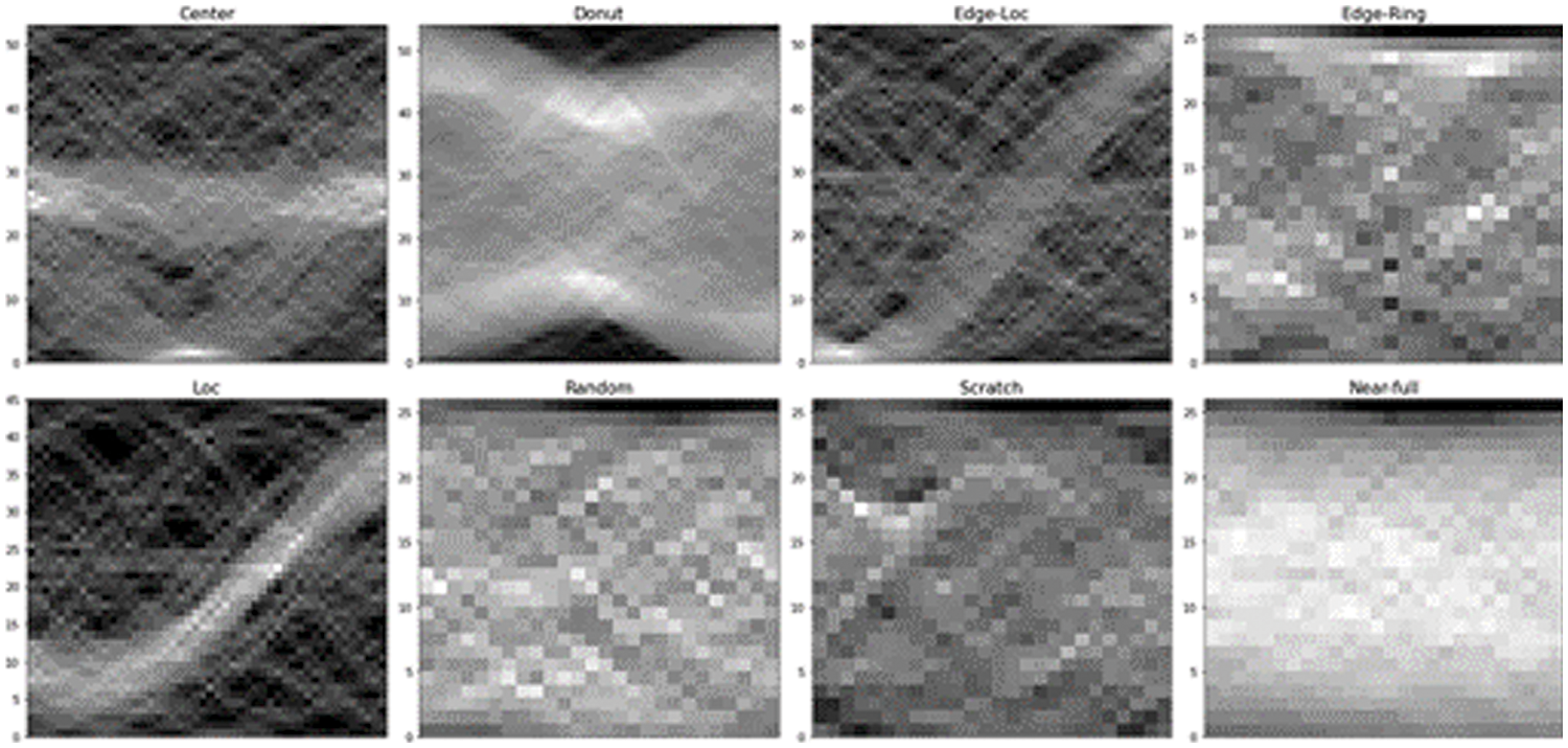
Figure 5: Radon-based images
Third, a geometry-based feature extraction technique is used to evaluate the geometric properties of each wafer map [41]. Geometry-based features have been derived by calculating local, statistical, and linear properties based on the analysis of various wafer map patterns and consultation with domain experts. The scale and rotation of these properties are invariant, and a region-labeling algorithm is used. The algorithm reveals the most prominent areas of the wafer defect pattern.
Fig. 6 shows the most prominent regions with the maximum area for each wafer map defect class. This function is also considered noise filtering to remove defect noise that is randomly present on the wafer map image. As a result, a total of 59 handcrafted features were extracted, containing 13 densities, 40 Radon shapes, and six geometric features, which were used to train the model.
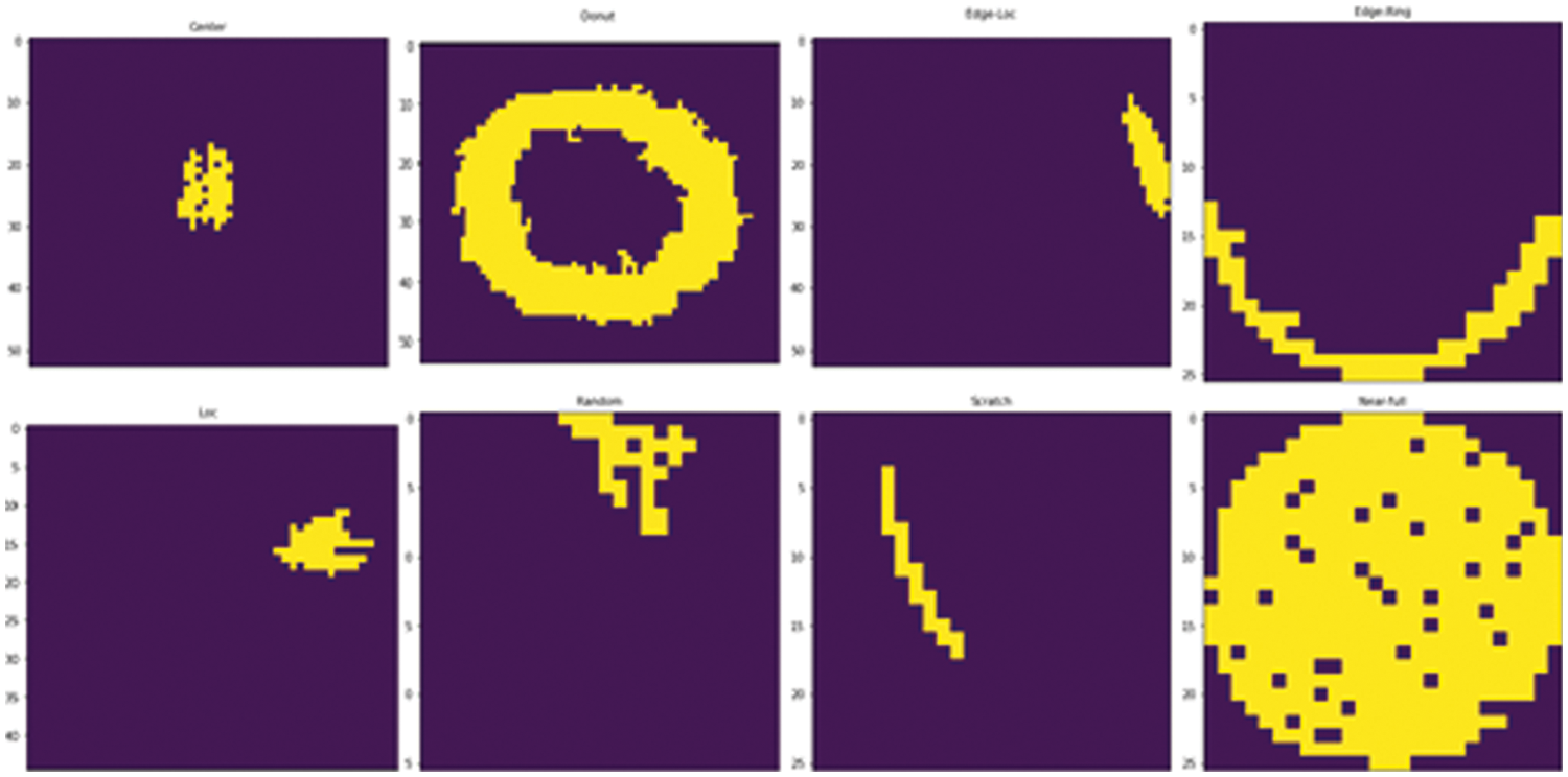
Figure 6: Geometry-based images
Fig. 7 shows the architecture of the BSEML model. In the proposed model, a base-level classifier was constructed using four ML classifiers: random forest (RF), decision tree (DT), KNN, and SVM. The meta-level classifier was constructed using the extreme gradient boosting classifier. The identification accuracy of the star base-level classifier depended on the wafer map defect class. Individual classifiers failed to achieve high accuracy as each classifier had its own learning capabilities and parameter values. Therefore, an ensemble approach of collecting the best results from all classifiers, aggregating them, and putting them in the meta-level classifier was used to obtain the final classification results for all defect classes. A summary of each individual classifier is as follows.
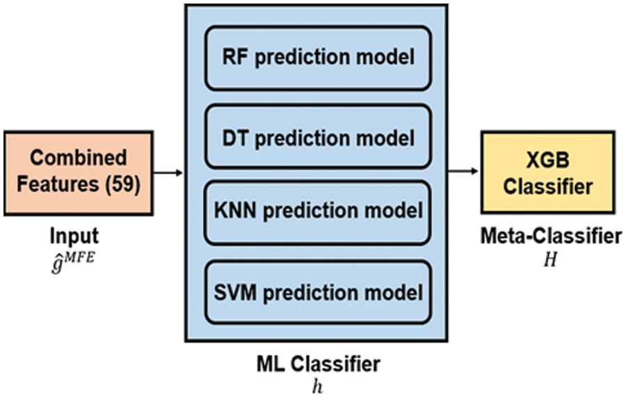
Figure 7: The architecture of the BSEML model
A decision tree (DT), also called a classification and regression tree used in both classification and regression analysis, is a classification model that divides the independent variable space while sequentially applying various rules. In predicting target variables or solving classification problems, the model enables checking which explanatory variable is the most important influencing factor and determines the detailed criteria for the prediction and classification of each explanatory variable [42].
A random forest (RF) is a bagging ensemble algorithm that trains several DT models and synthesizes the results to make the prediction. The bagging ensemble algorithm is a method of training individual DT models with a sampled dataset by allowing duplicates from the original dataset. In addition, DT is based on the principle of uncertainty called entropy, and the concept of entropy is expressed by the following expression [43].
KNN is an algorithm that is used to determine the classification of new data. The KNN for classification is expressed as follows [45].
For the input data
SVM is an algorithm that performs classification using support vectors and hyperplanes. The data are classified by maximizing the margin between the separated hyperplane and the support vector while minimizing the error [47]. Training by maximizing the margin may lead to some errors, but the classification accuracy is high for newly input data. Training by minimizing errors may lead to incorrect classification due to a narrow margin. The expression to maximize the SVM margin is as follows [48].
The proposed BSEML model is an ensemble technique combining base-level classifiers to improve prediction performance [50]. Based on the stacking ensemble structure, the error rate of individual classifiers is minimized. A stacking ensemble consists of a base-level classifier and a meta-level classifier. All base-level classifiers are trained with different approaches to perform target tasks using different learning algorithms. The data diversity of the ensemble model was improved by selecting different base-level classifiers with different parameter boundaries. Since the classifier selected this way was trained with the same extracted features, various predictive models were created with the same input data according to the decision boundary, thereby preserving the uniqueness of each classifier [33]. The meta-level classifier was trained to integrate the robustness of different base-level classifiers by verifying base-level classifier would be more accurate for each class of defects when performing the target task.
The base-level classifier output is then provided to the meta-level classifier to make final predictions [51]. In this study, extreme gradient boosting (XGB) was selected as a meta-level classifier to construct a boosted stacking ensemble.
XGB is the most popular algorithm in tree-based ensemble learning, which is based on the principle of boosting. A strong prediction model is built by weighing the learning error of the weak learner and reflecting it sequentially on the next learning model. Although the model is based on a gradient boosting machine (GBM), it works by solving the problems of slow execution time and lack of regularization, which are the weaknesses of GBM [52].
In this experiment, the meta-level classifier increased the accuracy of final predictions by applying weights to predictions of weak leaner models among basic classifiers and performing parallel learning. Tab. 2 shows the algorithm for the BSEML model.

Once the BSEML model is trained, it can be utilized to classify wafer map patterns. Given wafer map x as a new input, the predictive label y is derived by the following process. The wafer map x is augmented by the CAE model and enters
Eq. (8) shows the equation for the final class prediction. In
The WM-811K dataset, obtained in an actual industrial process, was used in this study; the dataset is publicly available in [54]. The dataset is a map of 811,457 wafers generated from over 40,000 detectors during circuit testing in the manufacturing process. Defect patterns were marked by domain experts in 172,950 wafer maps of theirs. For the experiment, only the wafer maps labeled in the dataset were used. A labeled wafer map belongs to one of the nine defect classes: Center, Donut, Edge-Ring, Edge-Local, Local, Random, Near-full, Scratch, and None. Each wafer map was checked in a two-dimensional array before being passed on to augmentation preprocessing.
As feature extraction was not possible for array elements with fewer than 100 defective elements, four abnormal wafer maps were removed. These four abnormal wafer maps were found to belong to the None class. Therefore, the number of datasets was reduced to 172,496. Tab. 3 shows the defect distribution in the labeled dataset. The None class defect occupies the most in the total. The shape of the wafer map varies from (26, 26) to (300, 300). The dataset obtained from the actual process has very few defect patterns and requires a lot of money and time. Therefore, 14,326 training datasets were extracted by randomly sampling from the labeled dataset. In order to apply the wafer map to a later process, all wafer maps were reshaped into (32, 32) where defect patterns were evenly distributed.

4.2 Convolutional Auto-Encoder for Data Augmentation
In the dataset acquired from the actual process, there is a difference in the amount of data for each defect class, and in severe cases, the data is biased toward only the majority class. Machine learning algorithms proceed with learning by assuming that each class has an equal ratio. As for a dataset with a class imbalance, machine learning does not perform precise learning and is biased toward the class which occupies a large proportion of the dataset [55].
The WM-811K used in this study has an imbalanced dataset. The None class accounts for more than 90% of the total defects, and there are insufficient defect patterns in the Donut and Near-full classes.
Therefore, in order to expand the number of defect images in the dataset and improve the generalization ability of the model, a data augmentation method based on CAE was used [56].
CAE is a variant of convolutional neural networks that is used as a tool for unsupervised learning of convolution filters [57]. CAE is usually applied in image reconstruction processes to minimize reconstruction errors by learning optimal filters. In AE, the images must be spread out as single vectors and the network must be designed regarding to the constraint on the number of inputs.
However, unlike normal AE that completely ignores the 2D image structure, CAE is a feature extractor that can learn even from two-dimensional images [58]. Fig. 8 shows the CAE parameters and architecture employed in this study. For each convolution 2D layer of the encoder and decoder of the CAE model, a kernel size of (3, 3) was used, and MaxPooling2D was applied. The kernel size of the pooling layer was (2, 2). ReLu was used for the activation functions of all layers, and a sigmoid for classification was used for the deconvolution layer at the end of the model. The entire process is explained as follows. The received input image data passes through the convolution layer while maintaining the spatial information in the encoder unit. The information passes through the layer, then through the central latent space layer, and finally through the decoder unit with noise added. The noise scale was set to 10% to minimize the effect on the defect pattern in this study [59].

Figure 8: The architecture of CAE model
4.3 Structural Similarity Index Measure Methods for Augmented Data Validation
SSIM was used to compare the difference between the original wafer image data and the augmented wafer image data. SSIM is a method designed to evaluate visual similarity rather than numerical error. SSIM specializes in deriving the structural information of the image and compares the degree of distortion of the structural information [60]. The SSIM equation is expressed as Eq. (9), and the following equations represent its internal equations [3].
In Eq. (10),
In Eq. (11),
In Eq. (12),
By comparing and analyzing raw image data and augmented image data with the SSIM scale, augmented image data with an SSIM value of 90% or more were used as feature extraction model input value [61]. Fig. 9 shows a comparison between the raw image and the augmented image.
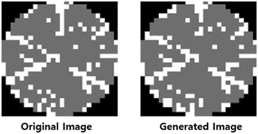
Figure 9: The comparison of generated image to the original image
In this study, a dataset of four cases was constructed from the training dataset for performance evaluation. Since the defect class is in a very unbalanced state in the original data, three augmentations were performed to solve this problem. Tab. 4 shows the wafer map data organized by enhancement ratio. Case 1 consists of raw wafer data as they are. Case 2 consists of a 30% augmented data from raw wafer data. Cases 3 and 4 consist of 40%, and 50% augmented data from raw wafer data, respectively. In addition, while performing data augmentation, the ratio of each defect pattern in the original data was maintained as much as possible. However, the None class was excluded from augmentation as it contained too much data compared to other defect classes. In each experiment, 80% of the data was used as the training dataset for the performance model, and the remaining 20% was used as the test dataset.

This experiment was performed using Python 3.6 in the Ubuntu 12.04 environment, and handcrafted feature extraction was obtained through the scikit-image library [62]. The scikit-learn library, Ensemble-Pytorch library, and XGBoost library were used together for training and comparison models [63–65].
Macro-average
where,
The confusion matrix is a table that supports the visualization of the performance of a trained classification algorithm in a classification problem. Each row of the matrix denotes an instance of the predicted class, and each column presents an instance of the actual class. The confusion matrix used in this experiment was normalized for effective analysis [67].
The proposed model was compared with two basic classifiers and four ensemble-based models. Tab. 5 shows the

Tab. 5 provides a comparison of
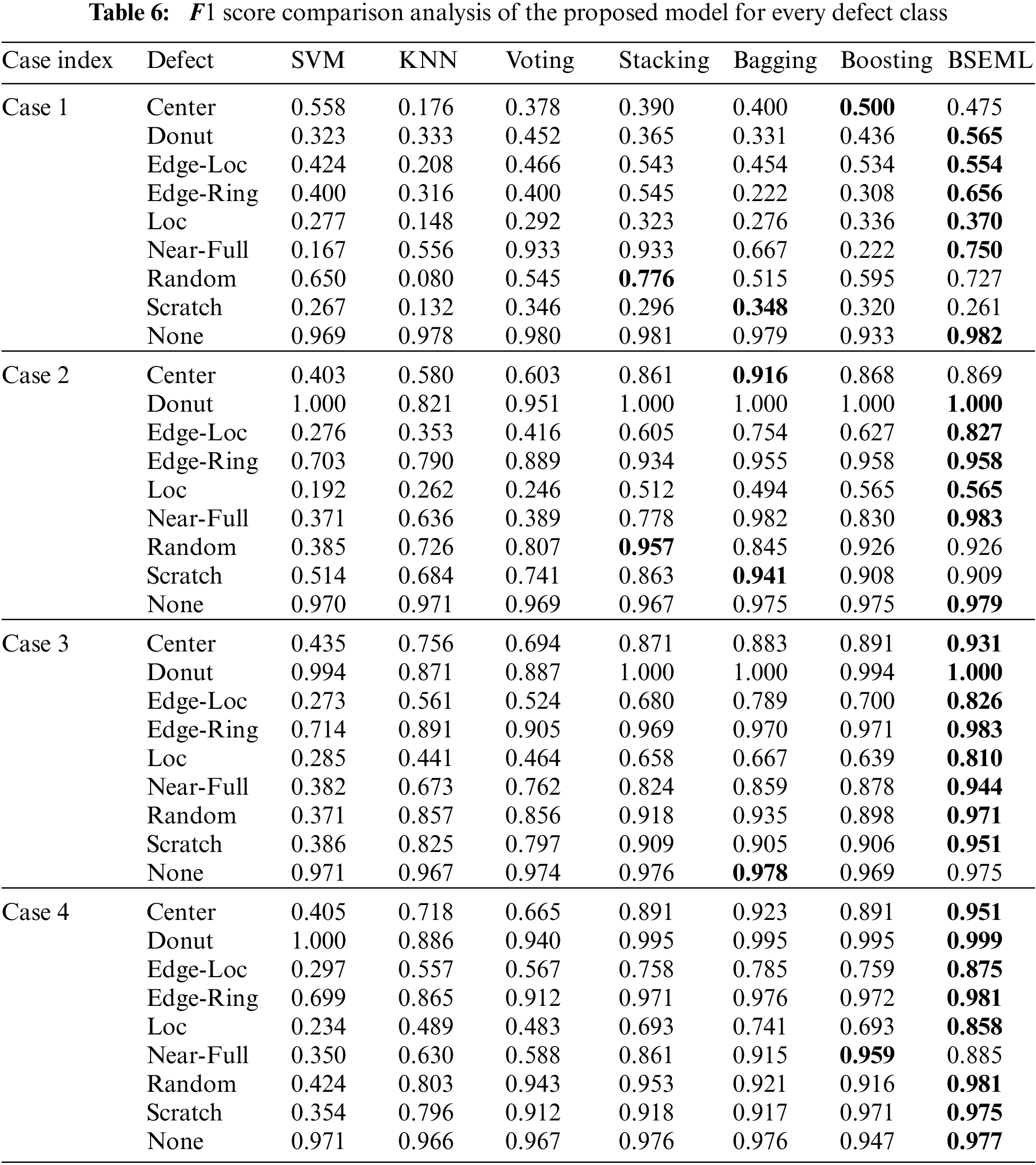
The proposed model presents good performance for all defect classes. Such results indicate that the proposed model increases the
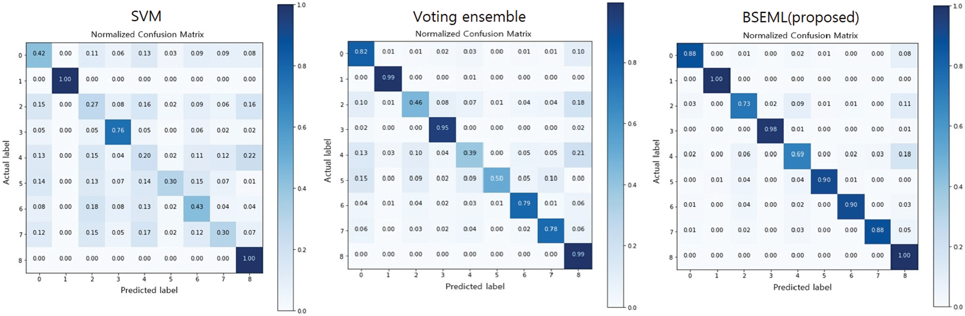
Figure 10: Confusion matrix of the baseline models and proposed model
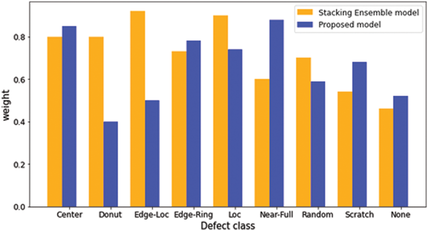
Figure 11: The comparison of weights for each defect classes
In this study, an algorithm that combines the reinforcement of insufficient defect patterns with an excellent hybrid model was proposed. The proposed method performs data augmentation using CAE on an image-type wafer map and features were subsequently extracted by applying density-based, geometry-based, and Radon-based feature extraction methods. This feature extraction technique improved the efficiency of the wafer defect identification system by providing detailed information about the wafer map and reducing the amount of computation required for learning. Then, four machine learning classifiers were stacked, and an ensemble model was built by using the XGB Classifier as a meta-level classifier. The proposed method demonstrated superior classification performance compared to those of the base-level classifier and ensemble models and showed robustness against insufficient defects. The effectiveness of the proposed method was verified experimentally using real data sets.
The improved classification performance demonstrated in this study is expected to have a significant effect on the stable automation of wafer map classification, leading to an improvement in product quality and yield in the actual semiconductor manufacturing process. Based on the proposed model, it will be possible to develop a model that guarantees robust performance while maintaining higher performance in various manufacturing domains, and it will also be possible to develop a model optimized for any domain by applying actual datasets from various manufacturing fields.
Funding Statement: This work was funded by the National Research Foundation of Korea (NRF) grant funded by the Korea government (MSIT) (No. NRF-2021R1A5A8033165) and the “Human Resources Program in Energy Technology” of the Korea Institute of Energy Technology Evaluation and Planning (KETEP) and was granted financial resources from the Ministry of Trade, Industry & Energy, Republic of Korea (No. 20214000000200).
Conflicts of Interest: The authors declare that they have no conflicts of interest to report regarding the present study.
References
1. T. Yuan, W. Kuo and S. J. Bae, “Detection of spatial defect patterns generated in semiconductor fabrication processes,” IEEE Transactions on Semiconductor Manufacturing, vol. 24, no. 3, pp. 392–403, 2011. [Google Scholar]
2. J. S. Fenner, M. K. Jeong and J. C. Lu, “Optimal automatic control of multistage production processes,” IEEE Transactions on Semiconductor Manufacturing, vol. 18, no. 1, pp. 94–103, 2005. [Google Scholar]
3. G. Hong and D. Suh, “Supervised-learning-based intelligent fault diagnosis for mechanical equipment,” IEEE Access, vol. 9, pp. 116147–116162, 2021. [Google Scholar]
4. N. G. Shankar and Z. W. Zhong, “Defect detection on semiconductor wafer surfaces,” Microelectronic Engineering, vol. 77, no. 3–4, pp. 337–346, 2005. [Google Scholar]
5. C. M. Tan and K. T. Lau, “Automated wafer defect map generation for process yield improvement,” in 2011 Int. Symp. on Integrated Circuits, Singapore, pp. 313–316, 2011. [Google Scholar]
6. R. Baly and H. Hajj, “Wafer classification using support vector machines,” IEEE Transactions on Semiconductor Manufacturing, vol. 25, no. 3, pp. 373–383, 2012. [Google Scholar]
7. W. Ming-Ju, J. -S. R. Jang and C. Jui-Long, “Wafer map failure pattern recognition and similarity ranking for large-scale datasets,” IEEE Transactions on Semiconductor Manufacturing, vol. 28, no. 1, pp. 1–12, 2015. [Google Scholar]
8. K. Jafari-Khouzani and H. Soltanian-Zadeh, “Radon transform orientation estimation for rotation invariant texture analysis,” IEEE Transactions on Pattern Analysis and Machine Intelligence, vol. 27, no. 6, pp. 1004–1008, 2005. [Google Scholar]
9. E. E. Schadt, C. Li, B. Ellis and W. H. Wong, “Feature extraction and normalization algorithms for high-density oligonucleotide gene expression array data,” Journal of Cellular Biochemistry, vol. 84, no. S37, pp. 120–125, 2001. [Google Scholar]
10. M. E. Mavroforakis and S. Theodoridis, “A geometric approach to support vector machine (SVM) classification,” IEEE Transactions on Neural Networks, vol. 17, no. 3, pp. 671–682, 2006. [Google Scholar]
11. F. -L. Chen and S. -F. Liu, “A neural-network approach to recognize defect spatial pattern in semiconductor fabrication,” IEEE Transactions on Semiconductor Manufacturing, vol. 13, no. 3, pp. 366–373, 2000. [Google Scholar]
12. B. Singh, S. S. Gleason, J. K. W. Tobin, T. P. Karnowski and F. Lakhani, “Rapid yield learning through optical defect and electrical test analysis,” Metrology, Inspection, and Process Control for Microlithography XII, vol. 3332, pp. 232–242, 1998. [Google Scholar]
13. S. P. Cunningham and S. Mackinnon, “Statistical methods for visual defect metrology,” IEEE Transactions on Semiconductor Manufacturing, vol. 11, no. 1, pp. 48–53, 1998. [Google Scholar]
14. K. Kyeong and H. Kim, “Classification of mixed-type defect patterns in wafer bin maps using convolutional neural networks,” IEEE Transactions on Semiconductor Manufacturing, vol. 31, no. 3, pp. 395–402, 2018. [Google Scholar]
15. J. -C. Chien, M. -T. Wu and J. -D. Lee, “Inspection and classification of semiconductor wafer surface defects using CNN deep learning networks,” Applied Sciences, vol. 10, no. 15, pp. 5340, 2020. [Google Scholar]
16. N. Yu, Q. Xu and H. Wang, “Wafer defect pattern recognition and analysis based on convolutional neural network,” IEEE Transactions on Semiconductor Manufacturing, vol. 32, no. 4, pp. 566–573, 2019. [Google Scholar]
17. M. Saqlain, B. Jargalsaikhan and J. Y. Lee, “A voting ensemble classifier for wafer map defect patterns identification in semiconductor manufacturing,” IEEE Transactions on Semiconductor Manufacturing, vol. 32, no. 2, pp. 171–182, 2019. [Google Scholar]
18. M. Piao, C. H. Jin, J. Y. Lee and J. -Y. Byun, “Decision tree ensemble-based wafer map failure pattern recognition based on radon transform-based features,” IEEE Transactions on Semiconductor Manufacturing, vol. 31, no. 2, pp. 250–257, 2018. [Google Scholar]
19. L. L. Y. Chen, K. S. M. Li, K. C. C. Cheng, S. J. Wang, A. Y. A. Hwang et al., “TestDNA-E: Wafer defect signature for pattern recognition by ensemble learning,” IEEE Transactions on Semiconductor Manufacturing, vol. 35, no. 2, pp. 373, 2022. [Google Scholar]
20. M. Fan, Q. Wang and B. van der Waal, “Wafer defect patterns recognition based on OPTICS and multi-label classification,” in 2016 IEEE Advanced Information Management, Communicates, Electronic and Automation Control Conf. (IMCEC), Xi An, China, pp. 912–915, 2016. [Google Scholar]
21. I. Naseem, R. Togneri and M. Bennamoun, “Linear regression for face recognition,” IEEE Transactions on Pattern Analysis and Machine Intelligence, vol. 32, no. 11, pp. 2106–2112, 2010. [Google Scholar]
22. M. -L. Zhang, J. M. Peña and V. Robles, “Feature selection for multi-label naive Bayes classification,” Information Sciences, vol. 179, no. 19, pp. 3218–3229, 2009. [Google Scholar]
23. S. Zhang, X. Li, M. Zong, X. Zhu and R. Wang, “Efficient kNN classification with different numbers of nearest neighbors,” IEEE Transactions on Neural Networks and Learning Systems, vol. 29, no. 5, pp. 1774–1785, 2017. [Google Scholar]
24. J. Yu and X. Lu, “Wafer map defect detection and recognition using joint local and nonlocal linear discriminant analysis,” IEEE Transactions on Semiconductor Manufacturing, vol. 29, no. 1, pp. 33–43, 2015. [Google Scholar]
25. S. Albawi, T. A. Mohammed and S. Al-Zawi, “Understanding of a convolutional neural network,” in 2017 Int. Conf. on Engineering and Technology (ICET), Antalya, Turkey, pp. 1–6, 2017. [Google Scholar]
26. R. Wang and N. Chen, “Defect pattern recognition on wafers using convolutional neural networks,” Quality and Reliability Engineering International, vol. 36, no. 4, pp. 1245–1257, 2020. [Google Scholar]
27. T. Nakazawa and D. V. Kulkarni, “Wafer map defect pattern classification and image retrieval using convolutional neural network,” IEEE Transactions on Semiconductor Manufacturing, vol. 31, no. 2, pp. 309–314, 2018. [Google Scholar]
28. T. Ishida, I. Nitta, D. Fukuda and Y. Kanazawa, “Deep learning-based wafer-map failure pattern recognition framework,” in 20th Int. Symp. on Quality Electronic Design (ISQED), Santa Clara, CA, USA, pp. 291–297, 2019. [Google Scholar]
29. C. -Y. Hsu and J. -C. Chien, “Ensemble convolutional neural networks with weighted majority for wafer bin map pattern classification,” Journal of Intelligent Manufacturing, vol. 33, no. 1, pp. 831–844, 2020. [Google Scholar]
30. T. -H. Tsai and Y. -C. Lee, “A light-weight neural network for wafer map classification based on data augmentation,” IEEE Transactions on Semiconductor Manufacturing, vol. 33, no. 4, pp. 663–672, 2020. [Google Scholar]
31. Q. Xu, N. Yu and F. Essaf, “Improved wafer map inspection using attention mechanism and cosine normalization,” Machines, vol. 10, no. 2, pp. 146, 2022. [Google Scholar]
32. P. P. Shinde, P. P. Pai and S. P. Adiga, “Wafer defect localization and classification using deep learning techniques,” IEEE Access, vol. 10, pp. 39969–39974, 2022. [Google Scholar]
33. R. Polikar, “Ensemble learning,” in Ensemble Machine Learning, Bostan, MA, USA: Springer, pp. 1–34, 2012. [Google Scholar]
34. G. Bonaccorso, “Important elements in machine learning,” in Machine Learning Algorithms, Birmingham, MB, UK: Packt Publishing Ltd., 2017. [Google Scholar]
35. G. Wang, J. Sun, J. Ma, K. Xu and J. Gu, “Sentiment classification: The contribution of ensemble learning,” Decision Support Systems, vol. 57, pp. 77–93, 2014. [Google Scholar]
36. H. Kang and S. Kang, “A stacking ensemble classifier with handcrafted and convolutional features for wafer map pattern classification,” Computers in Industry, vol. 129, pp. 103450, 2021. [Google Scholar]
37. O. Sagi and L. Rokach, “Ensemble learning: A survey,” Wiley Interdisciplinary Reviews: Data Mining and Knowledge Discovery, vol. 8, no. 4, pp. e1249, 2018. [Google Scholar]
38. X. Wang and K. K. Paliwal, “Feature extraction and dimensionality reduction algorithms and their applications in vowel recognition,” Pattern Recognition, vol. 36, no. 10, pp. 2429–2439, 2003. [Google Scholar]
39. M. Nixon and A. Aguado, “Image processing,” in Feature Extraction and Image Processing for Computer Vision, London, UK: Academic Press, pp. 83–136, 2019. [Google Scholar]
40. V. F. Leavers, “Use of the two-dimensional radon transform to generate a taxonomy of shape for the characterization of abrasive powder particles,” IEEE Transactions on Pattern Analysis and Machine Intelligence, vol. 22, no. 12, pp. 1411–1423, 2000. [Google Scholar]
41. R. M. Haralock and L. G. Shapiro, “Computer vision: Overview,” in Computer and Robot Vision, California, USA: Addison-Wesley Longman Publishing Co., Inc., 1992. [Google Scholar]
42. J. R. Quinlan, “Learning decision tree classifiers,” ACM Computing Surveys (CSUR), vol. 28, no. 1, pp. 71–72, 1996. [Google Scholar]
43. X. Li and C. Claramunt, “A spatial entropy-based decision tree for classification of geographical information,” Transactions in GIS, vol. 10, no. 3, pp. 451–467, 2006. [Google Scholar]
44. A. Paul, D. P. Mukherjee, P. Das, A. Gangopadhyay, A. R. Chintha et al., “Improved random forest for classification,” IEEE Transactions on Image Processing, vol. 27, no. 8, pp. 4012–4024, 2018. [Google Scholar]
45. S. Zhang, X. Li, M. Zong, X. Zhu and D. Cheng, “Learning k for kNN classification,” ACM Transactions on Intelligent Systems and Technology (TIST), vol. 8, no. 3, pp. 1–19, 2017. [Google Scholar]
46. G. Guo, H. Wang, D. Bell, Y. Bi and K. Greer, “KNN model-based approach in classification,” in OTM Confederated Int. Conf. on the Move to Meaningful Internet Systems, Catania, Italy, pp. 986–996, 2003. [Google Scholar]
47. T. Joachims, “Making large-scale SVM learning practical,” in Advances in Kernel Methods, London, England: Technical Report, pp. 169, 1998. [Google Scholar]
48. X. Huang, L. Shi and J. A. Suykens, “Support vector machine classifier with pinball loss,” IEEE Transactions on Pattern Analysis and Machine Intelligence, vol. 36, no. 5, pp. 984–997, 2013. [Google Scholar]
49. K. Lau and Q. Wu, “Online training of support vector classifier,” Pattern Recognition, vol. 36, no. 8, pp. 1913–1920, 2003. [Google Scholar]
50. M. Bieshaar, S. Zernetsch, A. Hubert, B. Sick and K. Doll, “Cooperative starting movement detection of cyclists using convolutional neural networks and a boosted stacking ensemble,” IEEE Transactions on Intelligent Vehicles, vol. 3, no. 4, pp. 534–544, 2018. [Google Scholar]
51. B. Pavlyshenko, “Using stacking approaches for machine learning models,” in 2018 IEEE Second Int. Conf. on Data Stream Mining & Processing (DSMP), Lviv, Ukraine, pp. 255–258, 2018. [Google Scholar]
52. T. Chen, T. He, M. Benesty, V. Khotilovich, Y. Tang et al., “Xgboost: Extreme gradient boosting,” R Package Version 0.4-2, vol. 1, no. 4, pp. 1–4, 2015. [Google Scholar]
53. V. B. Vaghela, A. Ganatra and A. Thakkar, “Boost a weak learner to a strong learner using ensemble system approach,” in 2009 IEEE Int. Advance Computing Conf., Patiala, India, pp. 1432–1436, 2009. [Google Scholar]
54. M. LAB, “WM-811k datasets,” in LSWMD Data (Accessed 12 July 2020). [Online]. Available: https://mirlab.org/dataSet/public. [Google Scholar]
55. H. Kaur, H. S. Pannu and A. K. Malhi, “A systematic review on imbalanced data challenges in machine learning,” ACM Computing Surveys, vol. 52, no. 4, pp. 1–36, 2020. [Google Scholar]
56. J. Luo, L. Wen, H. Fei, W. Cheng, Z. Shuo et al., “GPR B-scan image denoising via multi-scale convolutional autoencoder with data augmentation,” Electronics, vol. 10, no. 11, pp. 1269, 2021. [Google Scholar]
57. M. Chen, X. Shi, Y. Zhang, D. Wu and M. Guizani, “Deep features learning for medical image analysis with convolutional autoencoder neural network,” IEEE Transactions on Big Data, vol. 7, no. 4, pp. 750–758, 2017. [Google Scholar]
58. J. Masci, U. Meier, D. Cireşan and J. Schmidhuber, “Stacked convolutional auto-encoders for hierarchical feature extraction,” in Int. Conf. on Artificial Neural Networks, Berlin, Hidelberg, Germany, pp. 52–59, 2011. [Google Scholar]
59. M. S. Seyfioğlu, A. M. Özbayoğlu and S. Z. Gürbüz, “Deep convolutional autoencoder for radar-based classification of similar aided and unaided human activities,” IEEE Transactions on Aerospace and Electronic Systems, vol. 54, no. 4, pp. 1709–1723, 2018. [Google Scholar]
60. D. Brunet, E. R. Vrscay and Z. Wang, “On the mathematical properties of the structural similarity index,” IEEE Transactions on Image Processing, vol. 21, no. 4, pp. 1488–1499, 2011. [Google Scholar]
61. A. Hore and D. Ziou, “Image quality metrics: PSNR vs. SSIM,” in 2010 20th Int. Conf. on Pattern Recognition, Istanbul, Turkey, pp. 2366–2369, 2010. [Google Scholar]
62. V. Walt, S. Schönberger, J. L. Nunez, J. Boulogne, F. Warner et al., “Scikit-image: Image processing in Python,” PeerJ, vol. 2, pp. e453, 2014. [Google Scholar]
63. F. Pedregosa, G. Varoquaux, A. Gramfort, V. Michel, B. Thirion et al., “Scikit-learn: Machine learning in Python,” The Journal of Machine Learning Research, vol. 12, pp. 2825–2830, 2011. [Google Scholar]
64. Ensemble-PyTorch, 2021. [Online]. Available: https://ensemble-pytorch.readthedocs.io/. [Google Scholar]
65. XGBoost, 2016. [Online]. Available: https://xgboost.readthedocs.io/. [Google Scholar]
66. J. Opitz and S. Burst, “Macro f1 and macro f1,” arXiv preprint arXiv:1911.03347, 2019. [Google Scholar]
67. S. Visa, B. Ramsay, A. L. Ralescu and E. Van Der Knaap, “Confusion matrix-based feature selection,” MAICS, vol. 710, pp. 120–127, 2011. [Google Scholar]
68. J. Kozak and U. Boryczka, “Multiple boosting in the ant colony decision forest meta-classifier,” Knowledge-Based Systems, vol. 75, pp. 141–151, 2015. [Google Scholar]
69. V. K. Ayyadevara, “Gradient boosting machine,” in Pro Machine Learning Algorithms, Berkeley, CA, USA: Springer, pp. 117–134, 2018. [Google Scholar]
Cite This Article
 Copyright © 2023 The Author(s). Published by Tech Science Press.
This work is licensed under a Creative Commons Attribution 4.0 International License , which permits unrestricted use, distribution, and reproduction in any medium, provided the original work is properly cited.
 Downloads
 Citation Tools