DOI:10.32604/cmc.2022.024711
| Computers, Materials & Continua DOI:10.32604/cmc.2022.024711 | |
| Article |
Compact Multibeam Array with Miniaturized Butler Matrix for 5G Applications
1Department of Electrical Engineering, Bayero University, Kano, Nigeria
2Department of Electrical Engineering, Government College University Faisalabad, Pakistan
3Department of Electrical and Computer Engineering, COMSATS University Islamabad, Abbottabad Campus, Pakistan
*Corresponding Author: Muhammad K. Ishfaq. Email: mkamranishfaq@gcuf.edu.pk
Received: 28 October 2021; Accepted: 21 December 2021
Abstract: This paper presents the design and implementation of a miniaturized beam steering network that produces broadside beams when it is fed with a compact antenna array. Butler Matrix (BM) was used as the beam steering network. It was completely built from a miniaturized 3 dB hybrid-couplers in planar microstrip technology. It was configured by feeding the BM with a Planar Inverted-E Antenna (PIEA) array separated at 0.3 λ as against the 0.5 λ separation. This makes the BM produce a major radiation pattern at the broadside. Apart from the miniaturization, no modification was made from the BM side. However, employing effective mutual coupling reduction techniques helped to design the compact PIEA array. The validity of this BM based multibeam PIEA array was demonstrated by comparing the simulation results of the reflection coefficients, transmissions coefficients and the radiation pattern with measurements. The measurement results showed good agreement with simulations.
Keywords: Beam steering; compact; butler matrix; grating lobe; and mutual coupling; PIEA array
Beamforming arrays and multibeam antennas are key technology being employed in 5G to achieve high data rates. Multibeam antennas use beamforming networks (BFN) such as Rotman Lens and Butler Matrix (BM). Since the inception of the Butler matrix (BM) [1], researchers have put extensive effort into the realization of BM in a microstrip technique and other various technologies such as multi-layered [2], coplanar waveguide (CPW) [3], Swap port coupler [4], open-stubs [5], and substrate integrated waveguide (SIW) technology [6,7]. The design of Butler matrices in its classical form is based on transmission lines which are responsible for the bulky layout of the device. This is mostly due to the presence of fixed phase shifters, crossovers, and hybrid couplers employed in the design, with all their dimensions constrained by
The microstrip technique is the simplest method of realizing BM as presented in [9]. Recently, size miniaturization of BM at lower frequencies, becomes an active research area. In [10], a transmission line was replaced with artificial transmission lines to design a compact BM. The multi-layered packaging technologies are another option for realising a miniaturized BM as presented in [11]. Further size reduction of the BM using the advanced complementary metal-oxide-semiconductor (CMOS) technology was reported in [12]. A high level of miniaturization of the BM was achieved. In [13], a lumped element was used to replace the
Other researchers proposed a miniaturized BM by eliminating crossovers [14], elimination of phase shifters and crossovers [15]. In [16] coplanar-waveguide was reported, the coplanar-waveguide couplers utilize electromagnetic coupling via a slot in a common ground plane, therefore, the resulting circuit is without transmission line crossovers. A compact BM presented in [17] uses thin-film passive device technology. The complete BM was miniaturized by substituting the λ/4 transmission line (TL) with a bridged-T coil. With this technique, the size of the BM produced was drastically reduced without sacrificing the performance of the BM significantly. Lumped-element equivalent of λ/4 TL was applied in [4] using thin-film technology to produce a compact BM. Even though the circuit size reduces tremendously, but the bandwidth reduces proportionately because the conversion is usually applicable at a single frequency only. Another famous design problem of BM is that use of crossover points inevitable. To design a functional BM by avoiding crossing, a multi-layered technique is being used. This technique has the advantage of making the BM compact and at the same time eliminates the use of crossovers as proposed in [18].
The classical BM comprises of four hybrid couplers

Figure 1: 4 × 4 Butler matrix block diagram
In this paper, the design and implementation of a beam steering network along with a compact PIEA array that produces a broadside beam are proposed at 6 GHz for 5G applications. A miniaturized BM was implemented as the beam steering network that produces the broadside beam. This is contrary to the assertion made in [19] that it is not possible to use Butler matrices with
Butler Matrix was used as the beam steering network. It was designed from a miniaturized coupler, phase shifters and cross-overs.
2.1 Design of Miniaturized 3 dB Coupler
The design equations of the
The configuration of the coupler is shown in Fig. 2. P1 and P4 are the input and the isolation ports, whereas P2 and P3 serve as the output ports. All the lengths (L) represent the physical lengths of the sections as indicated in the Figure. To obtain the impedances of the coupler's such that their widths could be realised accurately, the curve in [20] was used. In this case, M was chosen to be

Figure 2: Schematic of the miniaturized coupler

Figure 3: (a) Layout of the miniaturized coupler and (b) S-parameter results of the coupler
These impedances and electrical lengths are used to obtain the physical lengths and widths of the coupler's lines and the stubs. The initial lengths and widths of the coupler have been optimized using a Genetic Algorithm (GA) embedded in the CST studio suit. The layout of the coupler is shown in Fig. 3a. The simulated S-parameter results showing the return loss and output phase difference are shown in Fig. 3b.
2.2 Design of Miniaturized 3 dB Coupler
This section explains the implementation of miniaturized crossover. It was implemented by cascading the two 90° miniaturized couplers. But sometimes, the resulting structure has to be optimized to obtain better results. Fig. 4 shows the schematic of the miniaturized cross over. The crossover was designed such that, when the input port of P1 is excited with a signal ‘A’, by applying standard hybrid analysis techniques, the signal emerges only at the diagonal port (P3) with, theoretically, no insertion loss. Practically, little power emerges from the remaining two ports P2 and P4.

Figure 4: Layouts of the miniaturized crossover
The miniaturized BM, crossover and phase shifters were used to form the proposed BM as explained in the next section.
2.3 The Proposed Butler Matrix
The miniaturized 3 dB coupler together with the crossovers designed in the previous section was used for the design of the miniaturized 4 × 4 BM. The design was done in a modular manner where every component is treated independently. One of the couplers from the input side of the BM was first simulated alongside with the

Figure 5: The miniaturized Butler matrix (a) The complete layout and (b) The photograph of the fabricated BM
Fig. 6a shows the scattering parameter results of the BM extracted from the full-wave simulator. The results presented are validated through measurement using a 4-port vector network analyser (VNA) and the performance characteristics obtained from the measured results of the BM by exciting all the ports separately are shown in Fig. 6b

Figure 6: Simulated and measured the reflection and transmission coefficients when (a) Port 1 and (b) Port 2 are excited
The progressive phase differences of the miniaturized BM are plotted and shown in Fig. 7. From this figure, the differential output phases correspond to excitation of port 1, are

Figure 7: S-parameter results show the output phase differences when each port is excited separately
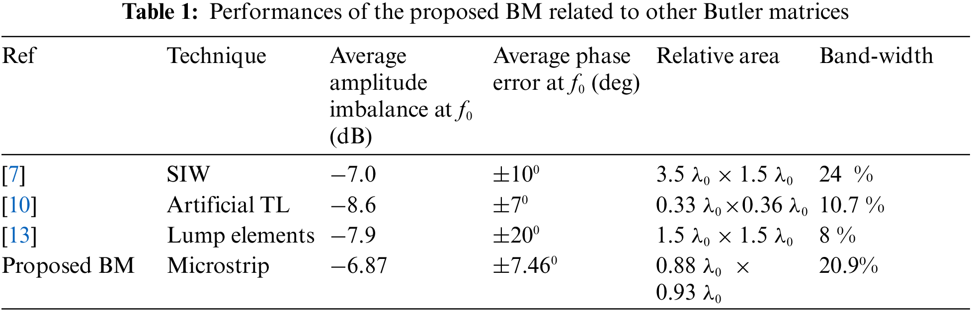
The performance of the proposed design has an average amplitude imbalance of −6.87 dB at the centre frequency. Compared with other designs in Tab. 1, the miniaturized BM have better amplitude imbalance and average phase error at the centre frequency than others, it can further be observed that, in terms of the relative area, [7,13] are larger than the proposed BM while [10] has a smaller area with the poorest bandwidth.
3 Planar Inverted-E Antenna Array
Firstly, a PIEA antenna was designed after an extensive parametric study and optimization. The top plate width, W, the length L, and the height h, are optimized to obtain the desired resonance frequency. The feed width, Wf is used to optimize enhanced bandwidth while the feed location Lb, is used to provide proper matching [21,22] at 6 GHz for 5G [23,24]. The air gap (εr = 1) of t = 0.5 mm between feed and ground. Figs. 8a and 8b shows the geometry, radiation pattern and the return loss of the single element PIEA antenna. From this figure, it can be observed that a return loss better than


Figure 8: (a) Single element PIEA (b) S11 and radiation pattern of the PIEA (c&d) PIEA array top & Bottom and (e) Array S-parameters
Further, Figs. 8c and 8d shows the configuration of the PIEA array, top and bottom respectively. The array design parameters are given in Tab. 2. The array is designed with 0.3

4 Multibeam Array Beam Steering Results
To further test the beam steering capability of the multibeam array, the miniaturized BM is integrated with the PIEA array as shown in Fig. 9. Unlike in the conventional spacing of the array on the BM, in this case, the inter-elements distance between the array is reduced to 0.3 λ due to the compact nature of the BM. When any port with a 135o phase shift is excited; it produced a very large back lobe, eventually resulting in the broad beam at zero degrees. In this case, the main beam becomes far away from the zero axis and therefore produces a very strong grating lobe, which overshadowed the main beam and is deposed at the broadside as depicted in Figs. 10 and 11.

Figure 9: Photograph of the miniaturized Butler matrix with antenna array under test

Figure 10: 3-D Radiation pattern from the compact multibeam array with miniaturized BM (a) Port 1 (b) Port 2 (c) Port 3 and (d) Port 4

Figure 11: Radiation pattern from compact multibeam array with miniaturized BM (a) Port 1 (b) Port 2 (c) Port 3 and (d) Port 4
Even though a BM with broadside beams was presented in [26], the BM has to be modified before realizing the broadside beam. The trick behind obtaining the broadsides beams in this paper was the compactness of the antenna array which eventually resulted in diminishing of the main lobe and enlargement of the back lobes. In this case, the main beam becomes far away from the zero axis and therefore produces a very strong grating lobe, which overshadowed the main beam and is deposed at the broadside. No modification was made from the BM side. However, due to the closeness among the array elements, mutual coupling and cross-polarization reduction techniques were effectively employed.
The radiation patterns result in three different formats; the 3-dimensional (3-D), polar and cartesian forms are extracted from the simulation software are processed and plotted alongside the measured patterns. The 3D patterns are shown in Fig. 10, while the polar radiation patterns are plotted in Fig. 11. When port 1 is excited with energy, the main beam angle is deposed at
The standard matrix utilizes 90° couplers and produces beams symmetrical to the broadside axis which leads to a shadowed area in this direction broadside direction. On the other hand, only the nonstandard matrix usually build from 180° hybrids produces a broadside beam. However, the structure of 180° rat-race hybrids and its topology is not suitable for use in the Butler matrix. Also, for the implementation of such type of BM in microstrip technology, the number of crossovers needed will greatly be increased which in turn will complicate the structure of the BM and introduce additional losses due to its complex structure and numerous bent lines at a 90° angle, especially at higher frequencies. This research succeeded to implement a BM completely build from 90° in planar microstrip technology that produces a broadside beam. This was achieved by feeding the BM with an antenna array separated by 0.3 λ. This makes the BM produce the main beam far away from the broadside axis and produces a very strong grating lobe that overshadowed the main beam and is deposed at the broadside. No modification was made from the BM side. However, few effective techniques in the array design were employed that helped to reduce the mutual coupling among the array elements due to their closeness. The validity of this BM was demonstrated by comparing the simulation results of the return losses, transmissions and radiation pattern with measurements, the measurement results showed good agreement with simulations. However, apart from little discrepancies between simulations and measured results of the s-parameters from the 4 × 4 BM all other results perfectly agreed.
Acknowledgement: The author acknowledges the research guidance and environment provided by Prof Sharul Kamal Abd. Rahim, Prof. Tharek Abd Rahman, Wireless Communication Centre, Universiti Teknologi Malaysia, and Prof. Mohamed Himdi, Institute of Electronics and Telecommunications of Rennes (IETR), University of Rennes I, France.
Funding Statement: The authors received no specific funding for this study.
Conflicts of Interest: The authors declare that they have no conflicts of interest to report regarding the present study.
1. J. Butler, “Beam-forming matrix simplifies design of electronically scanned antenna,” Electronic Design, vol. 9, pp. 170–173, 1961. [Google Scholar]
2. M. Traii, M. Nedil, A. Gharsallah and T. A. Denidni, “Novel UWB multilayer butler matrix,” in 2010 IEEE Antennas and Propagation Society Int. Symp., Toronto, ON, Canada, pp. 1–4, 2010. [Google Scholar]
3. M. Nedil, M. A. El Cafsi, T. A. Denidni and A. Gharsallah, “Novel UWB CB-CPW butler matrix for wireless applications,” in IEEE Antennas and Propagation Society, AP-S Int. Symp. (Digest): Memphis, TN, USA, pp. 1800–1801, 2014. [Google Scholar]
4. Y. S. Jeong and T. W. Kim, “Design and analysis of swapped port coupler and its application in a miniaturized butler matrix,” IEEE Transactions on Microwave Theory and Techniques, vol. 58, no. 4, pp. 764–770, 2010. [Google Scholar]
5. H. Hayashi, D. A. Hitko and C. G. Sodini, “Four-element planar butler matrix using half-wavelength open stubs,” IEEE Microwave and Wireless Components Letters, vol. 12, no. 3, pp. 73–75, 2002. [Google Scholar]
6. Q. L. Yang, Y. L. Ban, K. Kang, C. Y. D. Sim and G. Wu, “SIW multibeam array for 5G mobile devices,” IEEE Access, vol. 4, pp. 2788–2796, 2016. [Google Scholar]
7. A. A. M. Ali, N. J. G. Fonseca, F. Coccetti and H. Aubert, “Design and implementation of two-layer compact wideband Butler matrices in SIW technology for Ku-band applications,” IEEE Transactions on Antennas and Propagation, vol. 59, no. 2, pp. 503–512, 2010. [Google Scholar]
8. S. Aliyubabale, S. H. Lawan, S. K. A. Rahim and S. Ifeomaorakwue, “Implementation of 4 × 4 butler matrix using silver-nono instant inkjet printing technology,” in 2017 IEEE 3rd Int. Conf. on Electro-Technology for National Development, NIGERCON 2017, Owerri, Nigeria, vol. 2018-January, pp. 514–518, 2018. [Google Scholar]
9. T. N. Kaifas and J. N. Sahalos, “On the design of a single-layer wideband butler matrix for switched-beam UMTS system applications,” IEEE Antennas and Propagation Magazine, vol. 48, no. 6, pp. 193–204, 2006. [Google Scholar]
10. C. W. Wang, T. G. Ma and C. F. Yang, “A new planar artificial transmission line and its applications to a miniaturized Butler matrix,” IEEE Transactions on Microwave Theory and Techniques, vol. 55, no. 12, pp. 2792–2801, 2007. [Google Scholar]
11. S. C. Gao, L. W. Li, M. S. Leong and T. S. Yeo, “Integrated multibeam dual-polarised planar array,” IET Microwaves, Antennas and Propagation, vol. 148, no. 3, pp. 174–178, 2001. [Google Scholar]
12. T. K. G. Kwang and P. Gardner, “4 × 4 butler matrix beam forming network using novel reduced size branchline coupler,” in 2001 31st European Microwave Conf., London, UK, pp. 1–4, 2001. [Google Scholar]
13. E. Gandini, M. Ettorre, R. Sauleau and A. Grbic, “A Lumped-element unit cell for beam-forming networks and its application to a miniaturized Butler matrix,” IEEE Transactions on Microwave Theory and Techniques, vol. 61, no. 4, pp. 1477–1487, 2013. [Google Scholar]
14. K. Tekkouk, J. Hirokawa, R. Sauleau, M. Ettorre, M. Sano et al., “Dual-layer ridged waveguide slot array fed by a Butler matrix with sidelobe control in the 60-GHz band,” IEEE Transactions on Antennas and Propagation, vol. 63, no. 9, pp. 3857–3867, 2015. [Google Scholar]
15. S. A. Babale, S. K. Abdul Rahim, O. A. Barro, M. Himdi and M. Khalily, “Single layered 4 × 4 butler matrix without phase-shifters and crossovers,” IEEE Access, vol. 6, pp. 77289–77298, 2018. [Google Scholar]
16. M. Nedil, T. A. Denidni and L. Talbi, “Novel Butler matrix using CPW multilayer technology,” IEEE Transactions on Microwave Theory and Techniques, vol. 54, no. 1, pp. 499–507, 2006. [Google Scholar]
17. Y. S. Lin and J. H. Lee, “Miniature butler matrix design using glass-based thin-film integrated passive device technology for 2.5 GHz applications,” IEEE Transactions on Microwave Theory and Techniques, vol. 61, no. 7, pp. 2594–2602, 2013. [Google Scholar]
18. G. A. Adamidis, I. O. Vardiambasis, M. P. Ioannidou and T. N. Kapetanakis, “Design and implementation of single-layer 4 × 4 and 8 × 8 butler matrices for multibeam antenna arrays,” International Journal of Antennas and Propagation, vol. 2019, pp. 1–12, 2019. [Google Scholar]
19. R. Sorrentino and G. Bianchi, “Microwave and RF Engineering,” 1st ed., vol. 1. West Sussex, United Kingdon: John Wiley & Sons, pp. 224–230, 2010. [Google Scholar]
20. S. A. Babale and S. K. A. Rahim, “Miniaturized quadrature coupler using low-cost instant inkjet printing technology,” Microwave and Optical Technology Letters, vol. 59, no. 8, pp. 1819–1824, 2017. [Google Scholar]
21. H. T. Chattha, Y. Huang, M. K. Ishfaq and S. J. Boyes, “Bandwidth enhancement techniques for planar inverted-F antenna," IET Microwaves, Antennas and Propagation, vol. 5, no. 15, pp. 1872–1879, 2011. [Google Scholar]
22. M. Kamran Ishfaq, T. Abd Rahman, H. T. Chattha and M. Ur Rehman, “Multiband split-ring resonator based planar inverted-F antenna for 5G applications,” International Journal of Antennas and Propagation, vol. 2017, pp. 1–7, 2017. [Google Scholar]
23. D. A. Sehrai, F. Muhammad, S. H. Kiani, Z. H. Abbas and M. Tufail, “Gain-enhanced metamaterial-based antenna for 5G communication standards,” Computers, Materials & Continua, vol. 64, no. 3, pp. 1587–1599, 2020. [Google Scholar]
24. O. A. Saraereh and A. Ali, “Beamforming performance analysis of millimeter-wave 5G wireless networks,” Computers, Materials & Continua, vol. 70, no. 3, pp. 5383–5397, 2021. [Google Scholar]
25. S. Zhang, S. N. Khan and S. He, “Reducing mutual coupling for an extremely closely-packed tunable dual-element PIFA array through a resonant slot antenna formed in-between,” IEEE Transactions on Antennas and Propagation, vol. 58, no. 8, pp. 2771–2776, 2010. [Google Scholar]
26. M. Koubeissi, C. Decroze, T. Monediere and B. Jecko, “A new method to design a butler matrix with broadside beam: Application to a multibeam antenna,” Microwave and Optical Technology Letters, vol. 59, no. 1, pp. 35–40, 2006. [Google Scholar]
 | This work is licensed under a Creative Commons Attribution 4.0 International License, which permits unrestricted use, distribution, and reproduction in any medium, provided the original work is properly cited. |