DOI:10.32604/cmc.2022.023934
| Computers, Materials & Continua DOI:10.32604/cmc.2022.023934 | |
| Article |
Design of Low Power Transmission Gate Based 9T SRAM Cell
1Department of Electronics and Communication Engineering, Koneru Lakshmaiah Education Foundation, Vaddeswaram, Guntur, Andhra Pradesh, 522502, India
2Department of Electronics and Communication Engineering, Francis Xavier Engineering College, Tirunelveli,Tamil Nadu, 627003, India
3Department of Computer Science and Engineering, PSG Institute of Technology and Applied Research, Coimbatore, Tamil Nadu, 641062, India
*Corresponding Author: Md. Zia Ur Rahman. Email: mdzr55@gmail.com
Received: 27 September 2021; Accepted: 30 December 2021
Abstract: Considerable research has considered the design of low-power and high-speed devices. Designing integrated circuits with low-power consumption is an important issue due to the rapid growth of high-speed devices. Embedded static random-access memory (SRAM) units are necessary components in fast mobile computing. Traditional SRAM cells are more energy-consuming and with lower performances. The major constraints in SRAM cells are their reliability and low power. The objectives of the proposed method are to provide a high read stability, low energy consumption, and better writing abilities. A transmission gate-based multi-threshold single-ended Schmitt trigger (ST) 9T SRAM cell in a bit-interleaving structure without a write-back scheme is proposed. Herein, an ST inverter with a single bit-line design is used to attain the high read stability. A negative assist technique is applied to alter the trip voltage of the single-ended ST inverter. The multi-threshold complementary metal oxide semiconductor (MTCMOS) technique is adopted to reduce the leakage power in the proposed single-ended TG-ST 9T SRAM cell. The proposed system uses a combination of standard and ST inverters, which results in a large read stability. Compared with the previous ST 9T, ST 11T, 11T, 10T, and 7T SRAM cells, the proposed cell is implemented in Cadence Virtuoso ADE with 45-nm CMOS technology and consumes 35.80%, 42.09%, 31.60%, 12.54%, and 31.60% less energy for read operations and 73.59%, 93.95%, 92.76%, 89.23%, and 85.78% less energy for write operations, respectively.
Keywords: Bit-interleaving; low power; SRAM cell; schmitt trigger; transmission gate
As technology evolves each day, the important design constraints for transistor scaling are the speed and integrated density, while leakages and reliability issues degrade the overall device performances. Further scaling results in short-channel effects, and overcoming this effect has led to several leakage power reduction techniques in existing designs [1]. Electronic devices, like microprocessors and microcontrollers, require high performances based on low power and high speeds. Such devices may be packed compactly and handled easily but require a memory cell with a low power consumption [2,3]. A memory cell is a fundamental block in computer memory, and most digital devices are made using SRAM [4,5]. The high operating speed capability of SRAM makes it widely used over dynamic random-access memory (DRAM), even though SRAM designs are comparatively more complex. The SRAM memory cell is a flip-flop circuit and is typically implemented using metal oxide field-effect transistors (MOSFETs). SRAM plays an important role in the System on Chip (SoC) as it is the primary element in chip design. SRAM has a larger value of switched capacitance in the bit line (BL) and word line (WL), which requires a higher energy cost. Thus, reducing the power consumption on SRAM reduces the power consumption of SoC devices [6]. A MOSFET has three regions of operations: i) sub-threshold, ii) near-threshold, and iii) super threshold. In the sub-threshold region, the gate-to-source voltage is not as high as the edge voltage of a MOSFET, so this region is also called the cut-off region where the effects of current on the gate voltage are exponential. Conduction in the cut-off region is denoted as sub-threshold conduction, where there are more leakages even though the power consumption is low [7,8]. In the super threshold region, the gate-to-source voltage is greater than the MOSFET threshold voltage and is called the saturation region as there is no effect on the current with a greater drain voltage [9].
In the near-threshold voltage (NTV) region, the voltage of the gate-source is greater than the threshold voltage (Vth) of the MOSFET. Here, the current increases with the voltage at the drain terminal, and the current leakage is low compared to sub-threshold operations [10,11]. This results in greater improvements in reducing the power consumption compared to super threshold operations [12–14]. However, soft errors are induced in the near-threshold operation region due to the effects of alpha particles [15]. High-energy alpha particles interact with the memory cell and interrupt operations or even cause damage [16]. SRAM designs can be categorized based on interconnections with the inverter as i) cross-coupled standard inverter, ii) cross-coupled Schmitt-trigger (ST) inverter, and iii) cross-coupled ST inverter with a standard inverter. First, various inverters that fall under the cross-coupled standard inverter category are the conventional 6T [17], 8T [18], Pasandi's 9T [19], Chang's 9T [20], Joon's 10T [21], and 7T [22]. In 10T SRAM, a single BL is used for both read/write to reduce the power consumption [23], and in 11T, power gating transistors and a transmission gate are implemented to reduce the power leakage [24]. The read disturbance from BL or bit line bar (BLB) in the conventional 6T can flip the stored data. In 6T, the read and write stabilities are not achieved simultaneously because these depend on the beta- and alpha-ratios, respectively. The 7T SRAM cell is not affected by any RHSc issues and does not have any read disturbances that require low power. The advantages of cross-coupled ST inverters in SRAM designs over the standard inverter SRAM designs are i) the cross-coupled structure of the ST inverter with a standard inverter to improve the read stability, and ii) the ST inverter write assist scheme with selective power gating to improve the write capability. The ST 10T [25] and ST 11T [26] belong to the cross-coupled ST inverter group. In ST 11T, the cross-coupled ST inverter is connected with the read buffer, and a single BL structure is used for read operations, where the read buffer improves the hold and read stabilities. In the cross-coupled ST inverter with a standard inverter category, the ST 9T [27] has a single BL structure and is designed with WBSBS. Selective power gating is used to develop the write ability. The ST voltage of the 9T inverter can be controlled through the write-assist scheme. The MTCMOS method offers a high performance in low-power designs [28]. Transmission gates reduce the leakage power to a greater extent [29], and the ST inverter [30] provides a robust security and high read stability while the performance characteristic of the standard inverter decays for smaller supply voltages (Vdd). Based on several investigations, the literature suggests that current designs have problems, such as read/write stability and a reduced leakage power. To address these issues, the proposed method provides the following contributions.
• Compared to ST 10T, the proposed design has a large read stability as it uses a combination of standard and ST inverters.
• In place of single-pass gates in the literature, a transmission gate is implemented to reduce unnecessary switching during the hold mode.
• When a read disturbance reaches the storage node, the ST inverter is more resistant to read interruptions compared to ideal inverters.
• The proposed method holds column-based assist techniques to reduce the energy consumption.
• The read static noise margin of the proposed cell is high compared to the 10T SRAM and 6T SRAM cells.
The remainder of this work is organized as follows. Section 2 introduces the proposed TG-ST 9T SRAM design and its operation. Section 3 analyzes the performance of the proposed design with the N-curve metric. Section 4 compares the results with the ST 9T SRAM cell based on power and delay, and Section 5 concludes this article.
Several SRAM cell designs have been investigated to reduce the power, and significant constraints have been considered in the memory portion of the chip as the best possible design pathway, as described in the previous section. This section discusses the proposed SRAM cell design. The schematic and timing diagrams of the proposed SRAM cell are given in Figs. 1a and 1b. This method adapts the MTCMOS technique based on a single BL structure, which includes a high Vth with nominal Vth devices to reduce leakage. The proposed cell has a cross-coupled standard inverter and a single-ended modified ST inverter with both having high Vth. In place of a single-pass gate in the literature, a transmission gate (TP and TN) is used with one enable (EN) transistor connected between the two inverters, which reduces the unnecessary switching activities during hold mode. The TP, TN, and EN all have a nominal Vth. The word lines (WL and WLB) are row-based signals and the WWL is a column-based signal. The WL is connected to the TN and EN gates, the WLB is connected to the TP gate, and the WWL is connected to the source of the feedback transistor (NF).
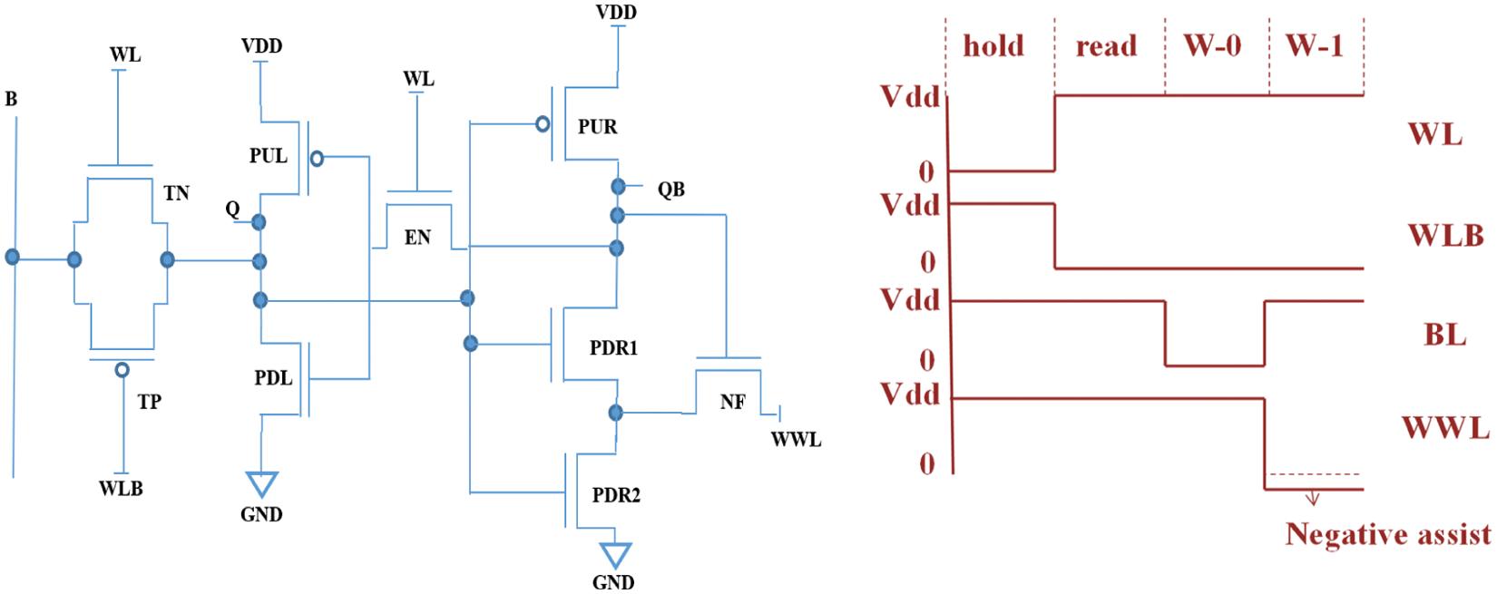
Figure 1: (a) Schematic and (b) Timing diagrams of the proposed SRAM cell
2.1 Proposed Method: Read Operation
The read operation of the proposed cell is depicted in Fig. 2. The BL is pre-charged to VDD during read operations, the WWL is set to “1,” and the inverter controls node Q. Activating the row-dependent signals (WL and WLB) allows turning on the transmission gate. If Q has zero charge, the BL discharges; otherwise, there is no change in the BL. Disturbances caused by the BL during read operations are the most common cause of read failures. If the storage node is enabled through read disturbances, then the voltage attains the inverter trip voltage. The proposed design addresses this problem by combining a regular inverter and an ST inverter into a cross-coupled structure. Figs. 3a and 3b represent the single-ended modified ST inverter and its DC characteristics, respectively. The ST inverter has a greater trip voltage than the normal inverter when the input changes from logical “0” to logical “1.” The voltage at node VX increases with the NF transistor, which reduces the strength of PDR1 transistor. As a result, when a read disturbance reaches the storage node, the ST inverter is more resistant to read interruptions compared with an ideal inverter.
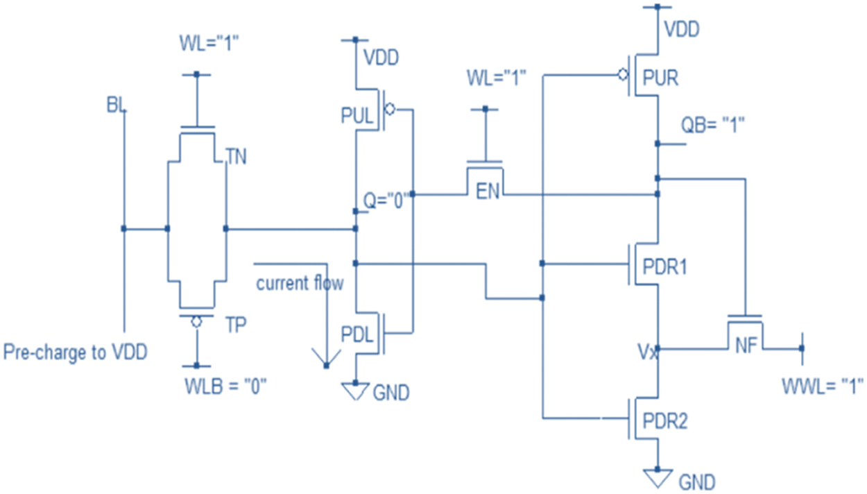
Figure 2: Read operations in the proposed ST inverter scheme
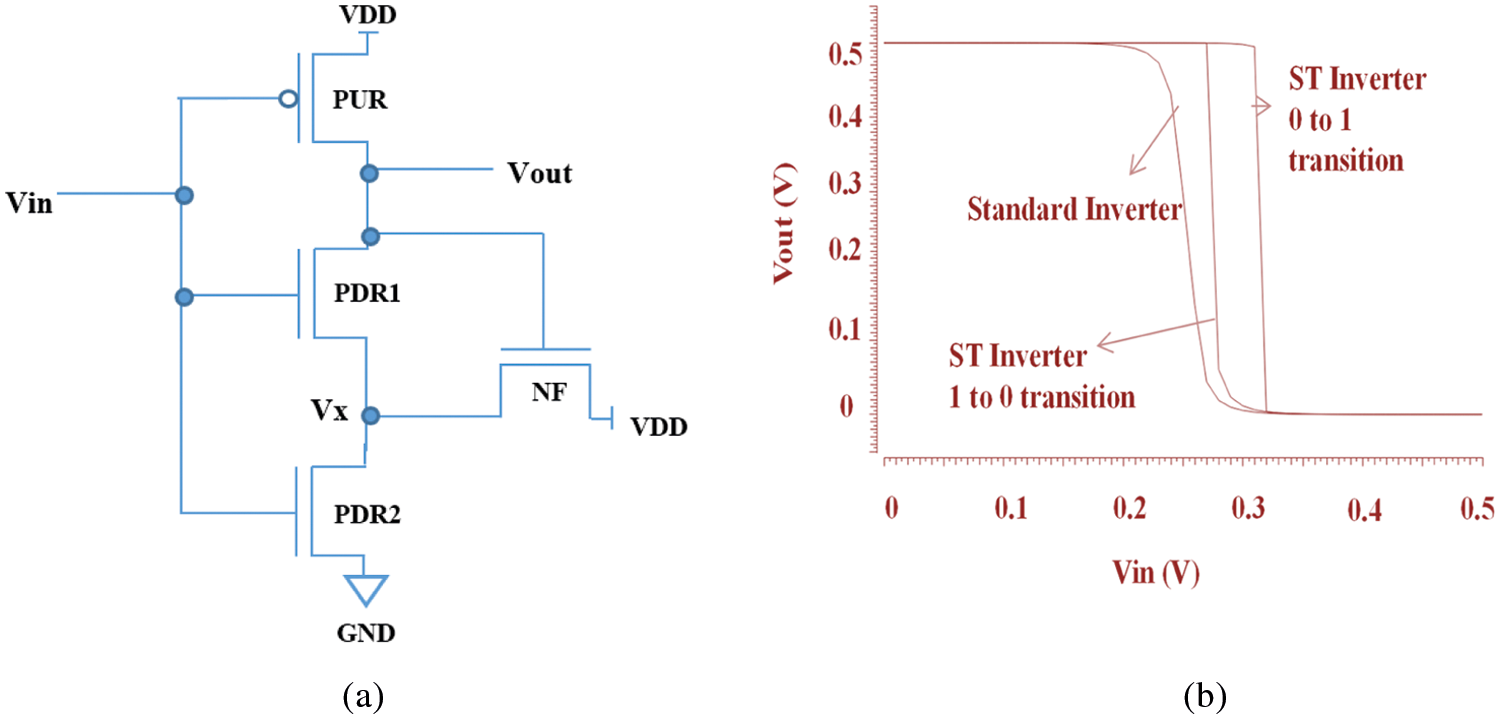
Figure 3: (a) Schematic diagram of the ST inverter and (b) Its DC characteristics at VDD = 0.5 V
Write operations are conditional on whether the information to be composed on the SRAM cell is a “1” or “0.” Fig. 4a illustrates the write-0 operation. The column-based signal WWL remains “1” in the write-0 operation, and the write driver sets BL to “0”, WL to “1,” and WLB to “0.” The Q node is pushed to “0” through the turned-on transmission gate, and the ST inverter flips. The proposed SRAM cell cuts off the VDD by disconnecting the pMOS transistor of the standard inverter, which achieves write-0 capability during the write operations.
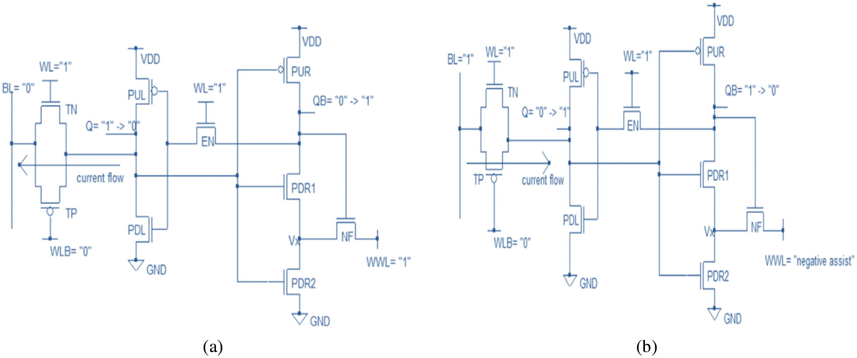
Figure 4: Proposed TG-ST 9T static RAM (a) Write-0 and (b) Write-1 operations
The write-1 process is illustrated in Fig. 4b. During write-1 operations, the write driver pushes the BL to “1,” the WL is ON, and the WLB is disabled. The proposed cell has a negative VWWL assist technique to boost its write-1 ability. Once the negative voltage is provided to the WWL, the turned-on feedback transistor NF drives the Vx node to a negative voltage. As the voltage at Vx decreases, the power of PDR1 increases and lowers the ST inverter trip voltage. As a result, the write-1 operation becomes more straightforward.
The amount of change in the trip voltage that corresponds to the increased PDR1 is shown in Fig. 5. When the column-based WWL signal is held at 0 V, the ST inverter trip voltage decreases by 16.61%. As the feedback function is removed by turning off the feedback transistor NF, the trip voltage is identical to that of a regular inverter. The trip voltage decrease to 64.85% using the negative assist technique on the column-based signal from the WWL. Lowering the trip voltage allows the negative assist technique to boost the write-1 ability.
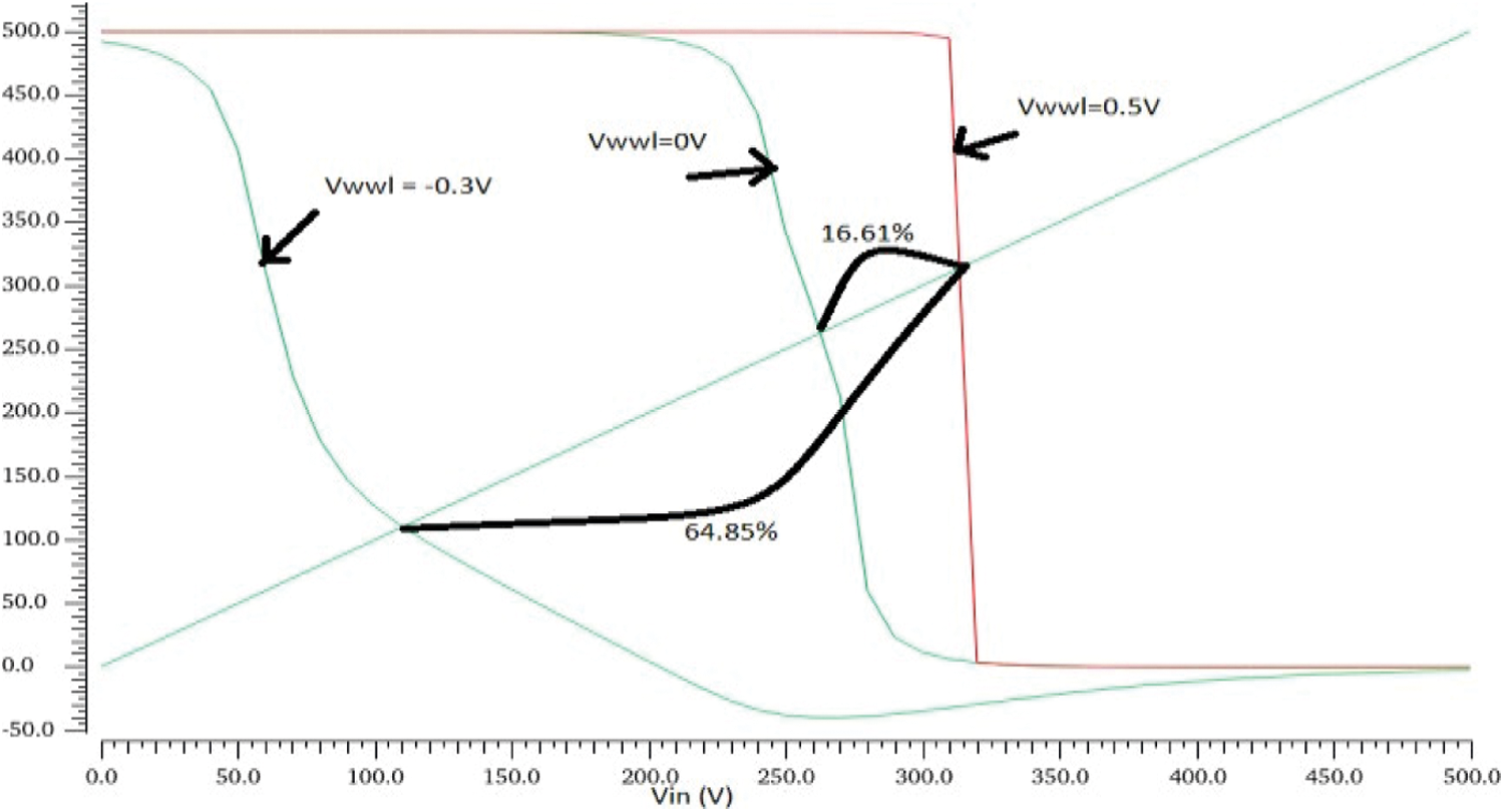
Figure 5: DC characteristics of the negative VWWL given at VDD = 0.5 V
The stability assessment and evaluation of the N-curve metric is implemented in the 7T, 10T, 11T, ST 11T, ST 9T, and the proposed TG-ST 9T SRAM cells.
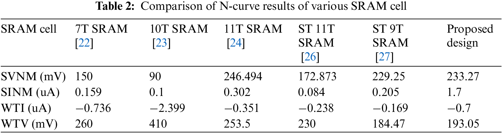
In the N-curve metric, the stability of the SRAM depends on the supply voltage. The SRAM cell becomes unstable if the supply voltage is reduced. The N-curve is the preferred metric to measure the stability of the SRAM. Drawing a butterfly/N-curve is a single plot with detailed information on the stability of the SRAM and write operation. For CR = 10, the stability parameters such as the static voltage noise margin (SVNM), static current noise margin (SINM), write trip current (WTI), and write trip voltage (WTV) are observed to provide reasonably better values compared to CR = 9, 8, and 7 in the 45-nm CMOS technology, as summarized in Tab. 1. Fig. 6 shows the N-curve of the proposed design, where the four N-curve parameters are utilized to characterize the device stability. Comparisons of the parameters SVNM, SINM, WTI, and WTV for the conventional SRAM cells (7T, 10T, 11T, ST 11T, ST 9T, and low leakage 10T) with the proposed method are given in Tab. 2.
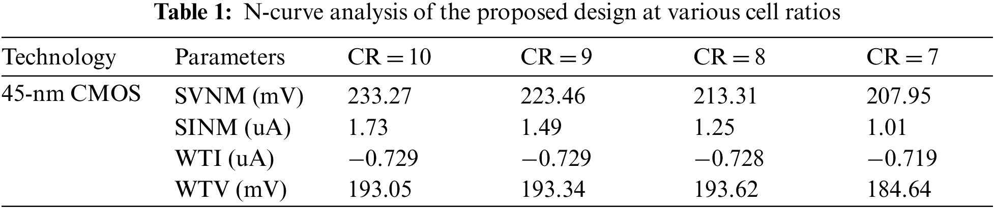
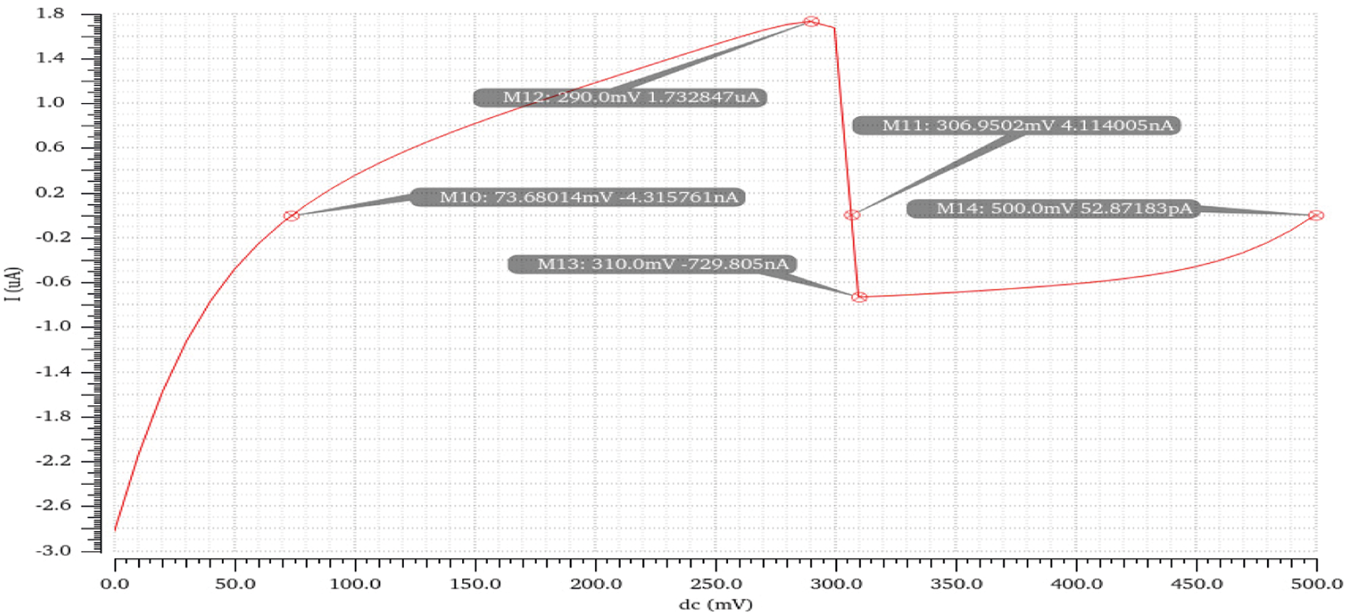
Figure 6: N-curve analysis of the proposed design at 0.5 V
The implementation results of the proposed TG ST-9T are compared with other SRAM cells using 45-nm CMOS technology. Monte Carlo simulations are performed in HSPICE to evaluate the SRAM cell design. Statistical analysis for the stability is achieved using the noise margin (NM), which is another key factor in SRAM cells and is an important constraint in their construction.
The time taken for the response when the input signal is applied to the WL is denoted as the read delay. Fig. 7 shows the read delay of the proposed design with various supply voltages of 0.40, 0.42, 0.44, 0.46, 0.48, and 0.50 V. A reduction in the delay between the ST 11T and ST 9T is the same as the reduction between the ST 9T and the proposed design with 0.44 and 0.40 V. Thus, it is perceived and verified that the design holds the minimum delay over the 7T SRAM.
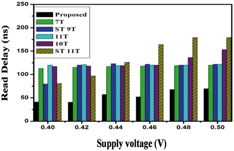
Figure 7: Read delay comparison at various supply voltages
Various write assist techniques have been proposed and used in several memory cell designs. Among the available write assist techniques, the suppressed cell VDD [31], raised cell VSS [32], boosted VWL [33], negative VBL [34], and negative VWWL assist techniques are commonly used in 7T, ST 11T, ST 9T, 11T, and 10T SRAM cells.
4.3 Half-Selected Cell Stability and Write Ability
All selected columns must be controlled in column-based assist techniques, which leads to an increased energy consumption, whereas only one row is selected and controlled in row-based assist techniques to attain a low power. Due to the low-energy in row-based support methods, the row-based boosted VWL is chosen with a boosted WL voltage to ensure the circuit has a 3σ stability. The negative VWWL for a 3σ write capability of the proposed and ST 9T SRAM cells are shown in Fig. 8, which indicates the proposed method has better results.
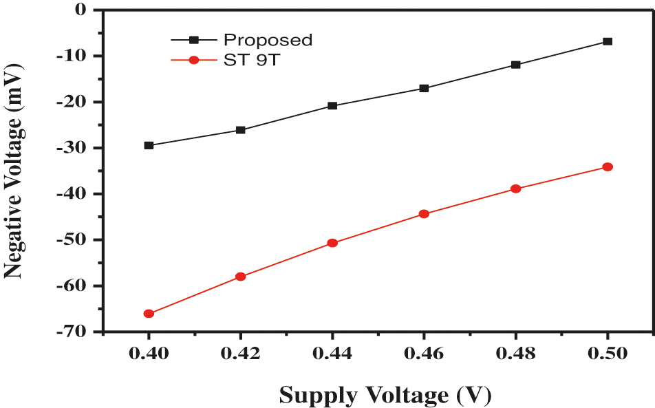
Figure 8: Comparison of the 3σ write capabilities for the negative VWWL and ST 9T SRAM cells
Monte Carlo simulations were implemented to estimate the write-0 and write-1 operations for each SRAM cell. Statistical simulations are performed using the static power loss of the proposed cell through the Monte Carlo distribution, as shown in Fig. 9. The waveforms for the control terminals with write-0 and write-1 procedures and the storage node at Vdd = 0.5 V are obtained from 1000 Monte Carlo simulations to verify the required functionality of the circuit.
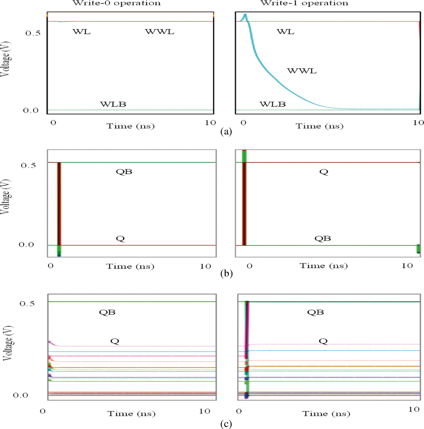
Figure 9: Write-0 and write-1 operational waveforms for (a) The control signals, (b) Selected cells in the storage node, and (c) Column-based cells
The leakage power of the proposed SRAM cell is compared with various SRAM cells at v = 0.5 V, as shown in Fig. 10a. As the ST inverter has a greater trip voltage than standard inverters, the SRAM cells that use cross-coupled ST inverters have higher hold stability yields than cross-coupled standard inverter SRAM cells. The leakage power of the proposed design has a maximum of 52.72% greater than the 7T SRAM cell, 82.16% greater than the 10T SRAM Cell, 77.27% greater than the 11T SRAM Cell, 50.83% greater than the ST 11T SRAM cell, and 36.72% lower than the ST 9T Cell due to the MTCMOS in the proposed design.
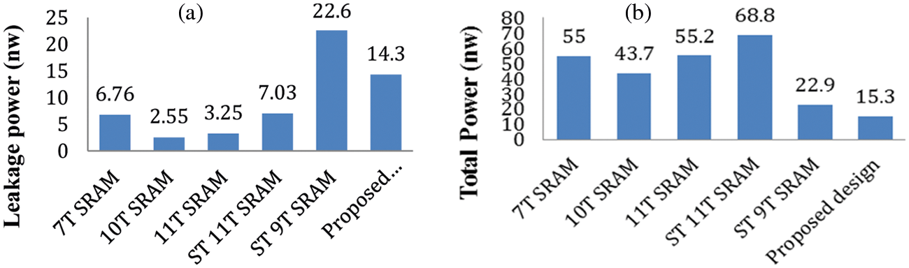
Figure 10: (a) Leakage power comparison of various SRAM cells and (b) Total power consumption at 0.5 V
A comparison of the total power consumption for the proposed SRAM cell with traditional cells is performed and shown in Fig. 10b. The proposed design has 72.18%, 64.98%, 72.28%, 77.76%, and 33.18% smaller power consumptions compared with the 7T, 10T, 11T, ST 11T, and ST 9T SRAM cells, respectively.
The proposed SRAM cell is implemented and simulated in the Cadence virtuoso environment for 45-nm CMOS technology. An energy-delay product (EDP) is commonly used to consider both the energy and efficiency. The power supply (Vdd) and EDP will not reflect the delay and energy values. Thus, these will be considered based on the power supply. Eqs. (1)–(3) show the EDP, static PDP, and PDP calculations, respectively. Tab. 3 shows simulations of the proposed and previous SRAM Cells at Vdd.
Tab. 3 indicates that the proposed Multi-Vt TG-ST 9T SRAM cell consumes a read energy of 50.2 nJ whereas the ST 9T, ST 11T, 11T, 10T, and 7T SRAM cells have read energies of 78.2, 86.7, 73.4, 57.4, and 73.4 nJ, respectively. The write energy of the proposed SRAM cell is 6.47 nJ and the ST 9T, ST 11T, 11T, 10T, and 7T SRAM consume 24.5, 107, 89.4, 60.1, and 45.5 nJ, respectively. Similarly, the total energy of the proposed SRAM cell design is 5.39 nJ and those for the ST 9T, ST 11T, 11T, 10T, and 7T SRAM are 24.8, 48.3, 32.1, 25.2, and 32.7 nJ, respectively. Thus, the proposed design has low read and write energies.
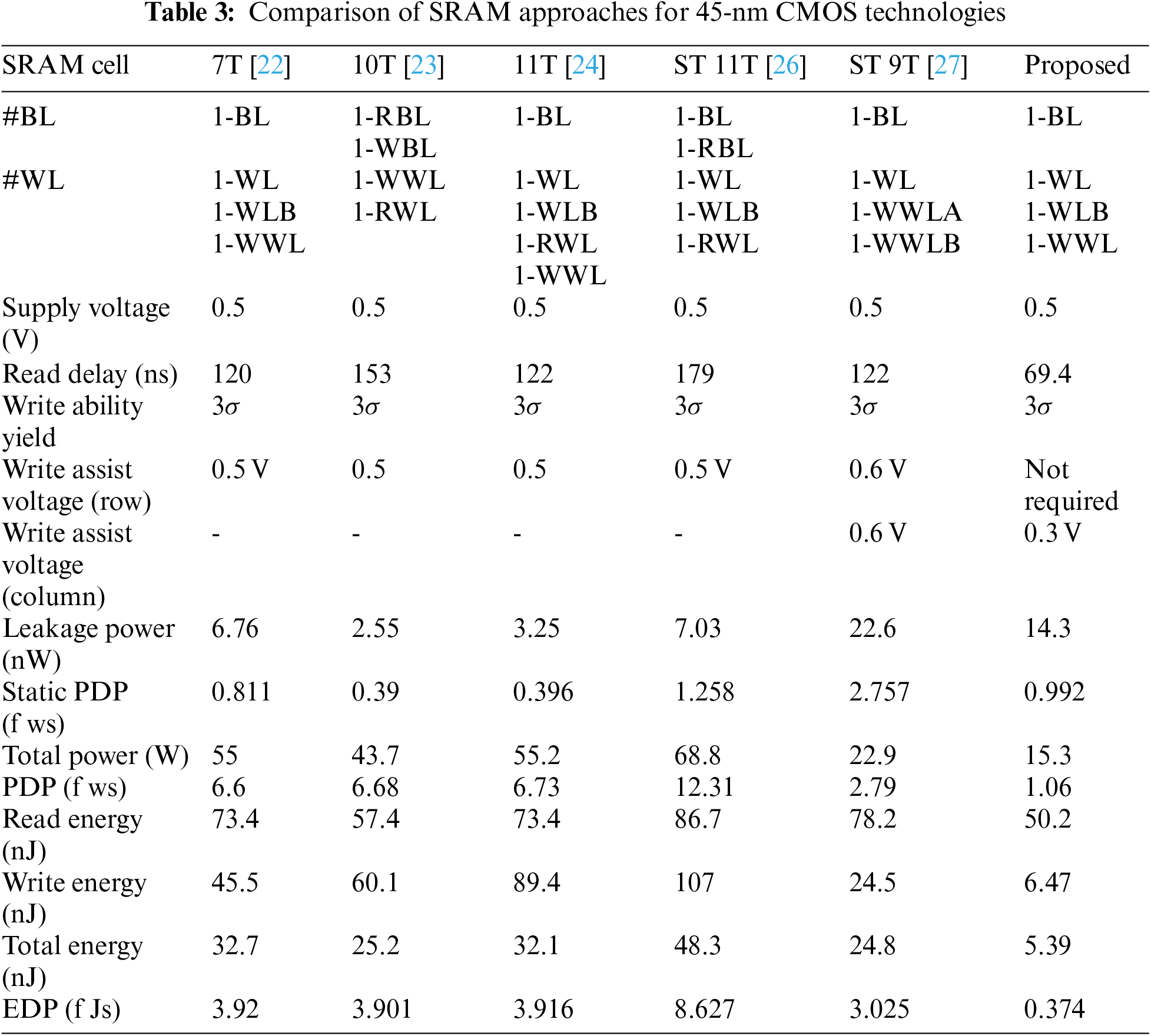
The increased power dissipation is due primarily to the scaling down of the system dimensions, input voltage, and threshold voltage. The proposed design uses a column-based assist technique to further reduce the energy consumption. The energy and delay are compared for the 7T SRAM, 10T SRAM, 11T SRAM, ST 11T SRAM, ST 9T SRAM, and the proposed design. The SRAM cell designs are simulated with 45-nm CMOS technology for a 0.5 V VDD using the Cadence Virtuoso ADE. Power reduction techniques such as the MTCMOS technique and transmission gate property allow the proposed design to reduce the power consumption and operate the SRAM cells faster. In the proposed method, the ST inverter with a single BL design is used to attain a high read stability. The proposed multi vt TG-ST improves the write ability yield using the negative VWWL write assist technique, which does not require a write assist row voltage. The total energy consumption is only 5.39 nJ and is lower than the ST 9T, ST 11T, and 7T SRAM cells. The proposed multi vt TG-ST 9T SRAM cell design has 87.63%, 95.66%, 90.44%, 90.41%, and 90.45% smaller EDPs than the ST 9T, ST 11T, 11T, 10T, and 7T SRAM cells, respectively, at a supply voltage of 0.5 V.
Funding Statement: The authors received no specific funding for this study.
Conflicts of Interest: The authors declare that they have no conflicts of interest to report regarding the present study.
1. R. G. Dreslinski, M. Wieckowski, D. Blaauw, D. Sylvester and T. Mudge, “Near-threshold computing: Reclaiming Moore's law through energy efficient integrated circuits,” in Proc. of the IEEE, USA, vol. 98, no. 2, pp. 253–266, 2010. [Google Scholar]
2. Y. Xie and J. Zhao, “Emerging memory technologies,” IEEE Micro, vol. 39, no. 1, pp. 6–7, 2019. [Google Scholar]
3. R. Praveena and S. Nirmala, “Bus encoded LUT multiplier for portable biomedical therapeutic devices,” Computers, Materials & Continua, vol. 53, no. 1, pp. 37–47, 2017. [Google Scholar]
4. A. Marjan and H. S. Azad, “Chapter one- introduction to non-volatile memory technologies,” Advances in Computers, vol. 118, pp. 1–13, 2020. [Google Scholar]
5. R. Praveena, “Enhanced portable LUT multiplier with gated power optimization for biomedical therapeutic devices,” Computers, Materials & Continua, vol. 63, no. 1, pp. 85–95, 2020. [Google Scholar]
6. V. P. -H. Hu, C. W. Su, Y. W. Lee, T. Y. Ho, C. C. Cheng et al., “Energy-efficient monolithic 3-D SRAM cell with BEOL MoS2 FETs for SoC scaling,” Electron Devices, vol. 67, no. 10, pp. 4216–4221, 2020. [Google Scholar]
7. T. Kim, S. Manisankar and Y. Chung, “A novel 8T cell-based subthreshold static RAM for ultra-low power platform applications,” Electronics. Article, vol. 9, no. 6, pp. 928, 2020. [Google Scholar]
8. S. Gupta, K. Gupta and N. Pandey, “PentavariateVmin analysis of a subthreshold 10T SRAM bit cell with variation tolerant write and divided bit-line read,” Circuits and Systems-I: Regular Papers, vol. 65, no. 10, pp. 3326–3337, 2018. [Google Scholar]
9. S. M. Sulaiman, B. Jaison and M. A. Bennet, “Performance of 7T SRAM using triple threshold voltage CMOS technology,” Pure and Applied Mathematics, vol. 119, no. 15, pp. 327–335, 2018. [Google Scholar]
10. K. Singh, B. Barry de, J. Hailong, H. Jos, C. Henk et al., “Converter-free power delivery using voltage stacking for near/subthreshold operation,” VLSI Systems, vol. 29, no. 6, pp. 1039–1051, 2021. [Google Scholar]
11. B. Pavankumar, “Analysis of high-performance near-threshold dual mode logic design,” Electronics and Telecommunications, vol. 65, no. 4, pp. 723–729, 2019. [Google Scholar]
12. S. Vangal, S. Paul, S. Hsu, A. Agarwal, R. Krishnamurthy et al., “Near-threshold voltage design techniques for heterogenous manycore system-on-chips,” Low Power Electronics and Applications, vol. 10, no. 2, pp. 1–23, 2020. [Google Scholar]
13. J. Park, H. Jeong, H. J. Kim and S. Jung, “Low power SRAM bit cell design for near-threshold operation,” in Proc. Int. Conf. on Consumer Electronics (ICCE), Asia, pp. 1–4, 2016. [Google Scholar]
14. J. Park, T. W. Oh and S. Jung, “pMOS pass gate local bitline SRAM architecture with virtual Vss for near-threshold operation,” VLSI Systems, vol. 28, no. 4, pp. 1079–1083, 2020. [Google Scholar]
15. H. Masanori, K. Kazutoshi, F. Jun, A. Shinichiro and W. Yukinobu, “Characterizing SRAM and FF soft error rates with measurement and simulation,” Integration, vol. 69, pp. 161–179, 2019. [Google Scholar]
16. M. S. M. Siddiqui, S. Ruchi, L. Van Le, T. Yoo, I. Chang et al., “SRAM radiation hardening through self-refresh operation and error correction,” Device and Materials Reliability, vol. 20, no. 2, pp. 468–474, 2020. [Google Scholar]
17. G. Torrens, B. Alorda, C. Carmona, D. Malag Ón-PeriÁnez, J. Segura et al., “A 65-nm reliable 6T CMOS SRAM cell with minimum size transistors,” Emerging Topics in Computing, vol. 7, no. 3, pp. 447–455, 2019. [Google Scholar]
18. N. Verma and A. Chandrakasan, “A 256 kb 65 nm 8T subthreshold SRAM employing sense-amplifier redundancy,” Solid-State Circuits, vol. 43, no. 1, pp. 141–149, 2008. [Google Scholar]
19. G. Pasandi and S. M. Fakhraie, “A 256-kb 9T near-threshold SRAM with 1k cells per bitline and enhanced write and read operations,” VLSI Systems, vol. 23, no. 11, pp. 2438–2446, 2015. [Google Scholar]
20. M. H. Chang, Y. T. Chiu and W. Hwang, “Design and iso-area Vmin analysis of 9T subthreshold SRAM with bit-interleaving scheme in 65-nm CMOS,” Circuits and Systems-II: Express Briefs, vol. 59, no. 7, pp. 429–433, 2012. [Google Scholar]
21. J. Chang, J. J. Kim, S. P. Park and K. Roy, “A 32 kb 10T subthreshold SRAM cell array with bit-interleaving and differential read scheme in 90 nm CMOS,” Solid-State Circuits, vol. 44, no. 2, pp. 650–658, 2009. [Google Scholar]
22. Y. Younghwi, J. Hanwool, S. SeungChul, W. Joseph, Y. Geoffrey et al., “Single bit-line 7T SRAM cell for near-threshold voltage operation with enhanced performance and energy in 14 nm FinFET technology,” Circuits and Systems I: Regular Papers, vol. 63, no. 7, pp. 1023–1032, 2016. [Google Scholar]
23. H. Banga and D. Agarwal, “Single bit-line 10T SRAM cell for low power and high SNM,” in Proc. Recent Innovations in Signal Processing and Embedded Systems (RISE), Bhopal, India, 2018. [Google Scholar]
24. R. Lorenzo and R. Paily, “Single bit-line 11T SRAM cell for low power and improved stability,” Computers & Digital Techniques, vol. 14, no. 3, pp. 114–121, 2020. [Google Scholar]
25. J. Kulkarni, K. Kim and K. Roy, “A 160 mV robust Schmitt trigger based sub-threshold SRAM cell,” Solid-State Circuits, vol. 42, no. 10, pp. 2303–2313, 2007. [Google Scholar]
26. S. Ahmad, M. K. Gupta, N. Alam and M. Hasan, “Single-ended Schmitt-trigger-based robust low-power SRAM cell,” VLSI Systems, vol. 24, no. 8, pp. 2634–2642, 2016. [Google Scholar]
27. C. Keonhee, P. Juhyun, T. Woooh and S. Jung, “One-sided Schmitt-trigger-based 9T SRAM cell for near-threshold operation,” Circuits and Systems I: Regular Papers, vol. 67, no. 5, pp. 1551–1561, 2020. [Google Scholar]
28. T. Tripathi, D. Chauhan, S. K. Singh and S. V. Singh, “Implementation of low-power 6T SRAM cell using MTCMOS technique,” Computer and Computational Sciences, vol. 11, no. 3, pp. 475–482, 2017. [Google Scholar]
29. P. Soumitra, G. Vivek, A. Islam and W. H. Ki, “Transmission gate-based 9T SRAM cell for variation resilient low power and reliable internet of things applications,” Circuits, Devices & Systems, vol. 13, no. 5, pp. 584–595, 2019. [Google Scholar]
30. P. R. Vijapur and B. V. Uma, “Single ended Schmitt trigger based 13T static random-access memory using FinFETs,” in Proc. Recent Trends in Electronics, Information & Communication Technology (RTEICT), India, pp. 744–748, 2018. [Google Scholar]
31. M. E. Sinangil, J. W. Poulton, M. R. Fojtik, T. H. Greer, S. G. Tell et al., “A 28 nm 2 Mbit 6 T SRAM with highly configurable low-voltage write-ability assist implementation and capacitor based sense-amplifier input offset compensation,” Solid-State Circuits, vol. 51, no. 2, pp. 557–567, 2016. [Google Scholar]
32. M. H. Tu, J. Y. Lin, M. C. Tsai, S. J. Jou and C. T. Chuang, “Single-ended subthreshold SRAM cell with asymmetrical write/read-assist,” Circuits and Systems I: Regular Papers, vol. 57, no. 12, pp. 3039–3047, 2010. [Google Scholar]
33. M. E. Mair and A. P. Chandrakasan, “A 28 nm high-density 6T SRAM with optimized peripheral-assist circuits for operation down to 0.6 V,” in Proc. Int. Solid-State Circuits Conf. (ISSCC), San Francisco, CA, USA, pp. 260–262, 2011. [Google Scholar]
34. Y. Fujimura, O. Hirabayashi, T. Sasaki, A. Suzuki, A. Kawasumi et al., “A configurable SRAM with constant-negative-level write buffer for low-voltage operation with 0.149 μm2 cell in 32 nm high-k metal-gate CMOS,” in Proc. Int. Solid-State Circuits Conf. (ISSCC), San Francisco, CA, USA, pp. 348–349, 2010. [Google Scholar]
 | This work is licensed under a Creative Commons Attribution 4.0 International License, which permits unrestricted use, distribution, and reproduction in any medium, provided the original work is properly cited. |