DOI:10.32604/cmc.2022.023017
| Computers, Materials & Continua DOI:10.32604/cmc.2022.023017 | |
| Article |
Design and Simulation of Ring Network-on-Chip for Different Configured Nodes
1Faculty of Engineering & Computer Sciences, Teerthanker Mahaveer University, Moradabad, Uttar Pradesh, 244001, India
2Faculty of Computers and Information, South Valley University, Qena, 83523, Egypt
3Department of Electrical and Electronics Engineering, School of Engineering, University of Petroleum and Energy Studies, Dehradun, 248007, India
4Department of Information Technology, College of Computers and Information Technology, Taif University, Taif, 21944, Saudi Arabia
5School of Engineering and Applied Sciences, Bennett University, Greater Noida, 201310, India
*Corresponding Author: Hammam Alshazly. Email: hammam.alshazly@sci.svu.edu.eg
Received: 25 August 2021; Accepted: 01 November 2021
Abstract: The network-on-chip (NoC) technology is frequently referred to as a front-end solution to a back-end problem. The physical substructure that transfers data on the chip and ensures the quality of service begins to collapse when the size of semiconductor transistor dimensions shrinks and growing numbers of intellectual property (IP) blocks working together are integrated into a chip. The system on chip (SoC) architecture of today is so complex that not utilizing the crossbar and traditional hierarchical bus architecture. NoC connectivity reduces the amount of hardware required for routing and functions, allowing SoCs with NoC interconnect fabrics to operate at higher frequencies. Ring (Octagons) is a direct NoC that is specifically used to solve the scalability problem by expanding each node in the shape of an octagon. This paper discusses the ring NoC design concept and its simulation in Xilinx ISE 14.7, as well as the communication of functional nodes. For the field-programmable gate array (FPGA) synthesis, the performance of NoC is evaluated in terms of hardware and timing parameters. The design allows 64 to 256 node communication in a single chip with ‘N’ bit data transfer in the ring NoC. The performance of the NoC is evaluated with variable nodes from 2 to 256 in Digilent manufactured Virtex-5 FPGA hardware.
Keywords: Ring NoC; FPGA synthesis; nodes communication; SoC design; integrated synthesis environment
Integrated circuits design and their manufacturing completely depend on the integration of different sub-modules, which are the pre-design block of the IP and cores [1] at the single chip. The property of reprocessing always resides in any ICs design. Manufacturing and semiconductors companies are working on the new challenges in the field of networks chip design and their throughput. The reuse of already developed submodules or functional blocks is a new idea to design the circuits having high performance in a shorter period having larger gate counts. The developed design based on the discussed formalities is called core-based or IP-based design or simple as SoC [2]. Many applications need architectures that are based on bus topological structures and bus-based architectures may be used to prevent the performance of these systems, as there is an increment in SoC-based IP modules [3]. The systems, which generally use bus-based communication [4], are not able to meet the requirement of bandwidth, power consumption, and latency. NoC [5] is the solution for such a communication-based system, which is a bottleneck for an embedded switching network to interconnect the different IP modules in SoCs. In comparison to the bus-based communication system, the bandwidth and design space is larger to maintain the arbitration mechanism and routing algorithms and their implementation strategies with different communication infrastructure. Moreover, NoC is very much helpful for fault tolerance [6] and enables SoC design engineers to search the suitable solutions for several system constraints and characteristics.
The current SoC system design [7] and development depends on most of the factors such as time to market, design time, design productively gap [8]. The current semiconductor and computer networking companies are looking the fast and reliable design and solutions in the field of computer nodes communication and technology using the single chip. The chip performance is estimated by many parameters such as delay, frequency of operation, power consumption and chip areas, and cost of design in the real-time system [9]. Most of the functionality of the system depends on the power requirements and frequency. The power is complete relating to the hardware and memory resources utilized by the system itself. NoC is the network version of the chip-based SoC [10] working in a multiprocessor environment. When the multiple nodes want to communicate in a real-time environment, there is the required scalable and feasible architecture that can be reprogrammed and used instead of the failure of any one of the nodes.
The rest of the paper is structured as follows. Section 2 discusses the related work. Section 3 explains ring NoC. The intercommunication logic is explained in Section 4. The results and discussion are reported in Section 5. Finally, Section 6 draws the paper conclusion.
The NoC is organized and structured by its topology [11], which includes the whole arrangement of routers and cores, as well as the ways used to comprehend routing, arbitration, buffering, flow management, and switching techniques [12]. The data flow control refers to the amount of data traffic or intensity that passes through the routers and channels. Routing [13] is a strategy or approach for determining the best path for a data or message from the transmitter to the desired end or receiver. The arbitration [14] mechanism assigns the scheduling or priority of tasks or sets the rules when multiple devices want to communicate with the master device at the same time or the same node requests multiple messages. Switching is the technique that defines how incoming traffic is accepted by a router and send to the output port of the router. In the last, buffering is the strategy or technique used to process and store data or messages in the case of a busy output channel. Hence, large-scale NoC design depends on routing, flow control, switching, and buffering. When multiple nodes are communicating in real-time, they are arranged in a specific topology. The topology is categorized as direct or indirect. Examples of direct topology are ring, torus, and mesh. Mesh is the highly used topology in NoC Communication. The 2D mesh [15] and torus topology follow the XY routing. The current manufacturing companies are looking for a reliable solution for NoC and application-specific routing algorithms [16]. Another important feature is that weather the network size is expandable in terms of nodes. The NoC chip time to market time depends on the design time of the NoC. If it takes a long time to launch the particular NoC in the market, there is no use in conducting research and meeting market deadlines.
NoC architecture has been used for the secured communication based on the cryptographic approach [17] by embedding encryption and decryption chip. The NoC was designed for the mesh, ring, and torus architectures, and comparative performance on FPGA was estimated based on supporting hardware and timing parameters. The designs were simulated on Modelsim and Xilinx software environments to check the functional behavior and data communication among nodes for Virtex-5 FPGA. The ZigBee wireless communication [18] supports star, mesh, and cluster trees. The hardware chip design and synthesis were carried on Virtex-5 FPGA, and data communication among all nodes was verified for the same topological NoC. The NoC strategy [19] has been proven one of the most efficient techniques for utilizing interconnections, and perform inter-communication between several nodes integrated on a single chip. The 2D NoC router was designed [20] using very-high-speed integrated circuit hardware description language (VHDL) and further applied for the implementation of the mesh NoC (4 × 4). Crossbar architecture (5 × 4) has been designed using VHDL [21] and simulated in Xilinx ISE 14.1 targeting Xilinx XC5VLX30-3 FPGA to validate the functionality of NOC on hardware. The 3D mesh NoC (4 × 4 × 4) was designed using VHDL in Xilinx ISE 14.2 and synthesized on Virtex-5 FPGA. The XYZ routing was used [22] for the identification of the nodes and the performance was evaluated based on FPGA hardware and timing parameters. The tree NoC [23] was designed using VHDL and synthesized on Virtex-5 FPGA. The FPGA resource details are very important for the designer to pre-estimate of the hardware resources for the specific chip. Machine learning [24] has been applied to estimate the accuracy of the FPGA hardware for mesh, star, and tree NoC, whose architecture was synthesized already on FPGA. Multilayer mesh NoC [25] was implemented in Xilinx ISE 14.2 in which the NoC was spitted into 8 layers and each layer was having 64 nodes to communicate with each other.
The contention-free Optical Ring Network-on-Chip (ORNoC) [26] was designed and constructed for scalable networks that supported 1296 nodes in 2D and 3D NoC. FPGA is utilized in data communication and telecoms switching applications such as dual-tone multifrequency (DTMF) and NoC [27]. The ring NoC has been realized as photonic integrated circuits (PIC) [28]. The performance of the bus-based and ring-based NoCs is compared, and it is projected that the ring NoC has demonstrated greater performance in terms of bit error rate (BER) than the bus-based NoC. The augment-based router buffered NoC [29] was designed for a reconfigurable ring architecture by manipulating the cycle decomposition of a torus bufferless network. In the runtime, the ring topologies were configured based on the performance of different cycle decompositions of the torus network to reduce the static power, and packet latency for accurate workloads. The ring network was used to build the neuromorphic-based NoC architecture [30]. The performance of the ring NoC was thoroughly assessed in terms of energy, latency, and resource utilization using three spike-based datasets, with neuromorphic architecture based on ring network yielding 18% improved results than mesh.
The practical applications of such networks can be realized for the hardware chip implementation of neuromorphic computing devices, wireless sensor networks nodes deployment, and different digital communication systems. NoC has been widely implemented for ASIC and FPGA realization. The common NoC are mesh, star, ring, tree, and hybrid, which are used based on application. Mesh NoC has been proven one of the reliable NoC for several embedded applications. Ring NoC is one of the well-established direct NoC that provides two-hop communication between any pair of nodes in the ring based on shortest route finding. The design can be extended for the large scale in which multiple nodes are arranged in a ring fashion and communicate with each other. The problem statement of the research work is to estimate the performance of the ring NoC with larger nodes and analyze the hardware and timing parameters on FPGA.
Ring topology is a well-known topology based on direct connections. The example of the ring NoC is an octagon, which is a simple structure in which 8 nodes communicate to each other with the help of 12 interconnecting links. The Octagon is shown in Fig. 1. The links are helping in the two ways communication of the structured NoC arranged in a ring shape [31]. It is following the easy and simple algorithm to choose the shortest path of routing. A switch is used to connect the nodes and establishes the communication [32] in multidimensional shape. Fig. 2 shows the examples of 64 nodes are shaped in the ring form. To address 64 nodes in ring form the addressing of 6 bit is required. It is started from “000000” as M0 for node 0 and ended with “111111” as M63 for node 63.

Figure 1: Ring NoC structure using 8 nodes

Figure 2: Ring NoC structure using 64 nodes [33]
Tab. 1 lists the addressing and behavior of router selection in the ring topological structure from node 0 to node 63 and corresponding routers as R0 to R63. All the nodes in the ring can communicate with each other. The node data packet has the data format in which the source node, destination nodes address is kept of 6-bit each, and 256-bit is the size of data. The inter-process communication is done by the ring-based NoC and corresponding architecture. Nodes are understood with the help of source address and destination address. For example, let node 1 wants to communicate with node 15 then the source address will be “000001” and the destination node address will be “00001111”. If a node wants to communicate with anyone, it has the probability to communicate with any of the target nodes as shown in Fig. 3.


Figure 3: Node-0 (000000) intercommunication to other nodes [33]
The packet data is transmitted from the source router to the target router. Fig. 4 shows the packet information having 6 bit defined for source router and 6-bit defined for target router. When multiple requests are arriving at one of the destinations, the priority based on first input first output (FIFO) logic is given to set the target nodes. The data of ‘n’ bit transfer is possible in-ring NoC but in our case, it is considered 256 bit.

Figure 4: Communication data format
The node logic diagram of the ring NoC architecture is shown in Fig. 5. The model supports the intercommunication of 64 nodes in real-time. From a hardware implementation point of view, each node associated with its processing elements is considered a memory element.
The data path architecture for the designing of 64 nodes needs a 6-bit source address. Therefore, a decoder of size (6 × 64) is needed to decode the address. All nodes are accessed with their source address and decoder unit. A node can communicate to one node at a time for that (64 × 1) demultiplexer is used to select the output node or destination node. The destination node is also identified with the help of a 6-bit node address. The memory unit has 64 registers of the length of data width. These registers are selected with their address of 6-bit. To write the data in the register the write_en control signal is enabled and reading of data is done with the help of signal read_en. The data writing and reading is taken place concerning node address as source_address and destination_address.

Figure 5: Datapath logic diagram [33]
The register transfer level (RTL) view of the 2D ring network is shown in Fig. 6 and its internal schematic is shown in Fig. 7. The top view representation of the developed design corresponds to its pins details and input/output logic is presented with the help of RTL schematics [34]. The inputs and outputs of the RTL form the entity of the chip. Tab. 2 explains the pin details of ring NoC. The functional simulation of the ring network topological NoC is shown in Fig. 8. The Fig. 9 presents the Modelsim result simulation of 256-bit data in ASCII for ring NoC. The simulation presents the data transfer from source node N1 to destination node N8. The Modelsim software functional simulation is using the inputs given.

Figure 6: RTL view of ring NoC

Figure 7: Internal schematic of ring NoC

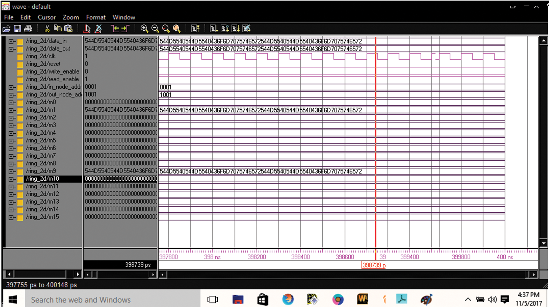
Figure 8: Modelsim result simulation of 256-bit data in hexadecimal for ring NoC
Step 1: Set the value of reset to ‘1’ and execute the program; all node data will have zero output.
Step 2: Set the value of reset to zero and apply a clock pulse on the rising edge. With input data, force the values of source address, destination address, and the data value of the destination node, then run.
Step 3: Set the address as the source address and destination address of destination nodes, as well as the input data packet on the input source, and run it. The flow chart of the simulation process is given in Fig. 10.
Test Data (Ring): First reset = ‘1’ and run. It will make all the router or nodes data to zero. Then reset = ‘0’ and give direct positive clock signal. Assign the Write_en = ‘1’, in_node_address = “000001” out_node_address = “001001”, based on output node, data_in = “54 4D 55 40 54 4D 55 40 43 6F 6D 70 75 74 65 72 54 4D 55 40 54 4D 55 40 43 6F 6D 70 75 74 65 72” in hexadecimal or TMU@TMU@ComputerTMU@TMU@Computer in ASCII. The same data is from source node M1 <255:0>. When Write_en = ‘0’, Read_in = ‘1’, the destination node M9 <255:0> and data_out< 255:0> are getting the same data. Data_out = “0101 0100 0100 1101 0101 0101 0100 0000 0101 0100 0100 1101 0101 0101 0100 0000 0100 0011 0110 1111 0110 1101 0111 0000 0111 0101 0111 0100 0110 0101 0111 0010 0101 0100 0100 1101 0101 0101 0100 0000 0101 0100 0100 1101 0101 0101 0100 0000 0100 0011 0110 1111 0110 1101 0111 0000 0111 0101 0111 0100 0110 0101 0111 0010” in binary.

Figure 9: Modelsim result simulation of 256-bit data in ASCII for ring NoC
The device utilization summary [35] shows the percentage of hardware that was used in the chip design and synthesis. The timing report calculates the shortest and longest time to reach the output. Timing parameters are used to provide more information on delay parameters such as the minimum period time, the minimum input arrival time before the clock, and the maximum output necessary time after the clock. The synthesis report generated by Xilinx software displays the exact information of device utilization as well as a summary of timing. The details relating to the hardware and timing summary are included in Tabs. 3 and 4 respectively. Fig. 11 presents the hardware usage graph with different cluster sizes in the ring NoC in Virtex-5 FPGA. Fig. 12 presents the timing graph with different cluster sizes in the ring NoC.

Figure 10: Flow chart for ring NoC


Figure 11: Hardware utilization with cluster size in the ring NoC

Figure 12: Timing values with cluster size in the ring NoC
The Virtex-5 (XC5VLX110T) FPGA supports up to 680 users I/Os with a wide selection of I/O standards from 1.2 V to 3.3 V at 550 MHz. It is having 65-nm Copper CMOS process processing technology with 1.0 V core voltage and 12-layer metal provides extreme routing capability and accommodates hard-IP immersion. The triple oxide technology provides reduced static power consumption with 10-bit ADC. In the FPGA verification, the .bit file of the configured ring NoC is burned into FPGA with the help of input switches as the address of the source and destination node. The logic synthesis is carried out after the logic implementation, routing, and placement into the FPGA device. The data communication is verified on the corresponding LEDs with ‘1’ and ‘0’ logic. The comminated data of the destination nodes is verified on the LED byte by byte.
In comparison to Ref. [33], the designed chip is optimal in terms of slices, flip flops, and memory hardware utilization. The designed NoC supported 625 MHz frequency with 20.195 ns delay. The existing design supported 535.733 MHz on Virtex-5 FPGA with 263208 kB memory. The designed chip is having greater frequency support with optimal delay implying a faster response in comparison to the existing design. The designed chip supported ‘N’ bit data communication whereas the existing design is limited to 16-bit data.
The ring NoC hardware chip design was completed successfully in Xilinx ISE 14.7 software, and the design was carried out for 64 nodes. The nodes are identified as node 0 (000000) to node 63 (111111). Similarly, the nodes are numbered as node-0 (00000000) to node-255 (11111111). The RTL depicts all of the design's pins in detail, while the Modelsim functional simulation depicts successful data flow between the nodes. The design concept is scalable, and it may be extended to a large number of nodes to configure individual applications, according to the current stage of the work. The NoC design offers 64 nodes at 230 MHz and 256 nodes at 625 MHz, indicating faster switching for high-speed embedded applications. For 64 and 256 nodes, the predicted combinational latency is 16.235 ns and 20.915 ns, respectively. The design supports ‘N’ bit data communication and 256-bit data is verified in simulation and synthesis. The hardware and timing values are also seen to increase as the cluster size of the NoC increases, which will certainly increase as the number of nodes grows. When the nodes communicate in a larger network, security becomes an issue. The NoC hardware maintains optimal network performance and security can be addressed by integrating different encryption and decryption algorithms at transmitting and receiving ends. We intend to incorporate the notion of hardware chip security in the future by incorporating cryptographic encryption and description in the hardware chip itself. The network-on-chip attacks detection and security can be addressed by embedding the security algorithms so that the NoC can be applicable for high-speed communication and security requirements such as in 5G communication and cloud computing.
Funding Statement: This work was supported by the Taif University Researchers Supporting Project, Taif University, Taif, Saudi Arabia, under Grant TURSP-2020/26.
Conflicts of Interest: The authors declare that they have no conflicts of interest to report regarding the present study.
1. P. K. Sahu and S. Chattopadhyay, “A survey on application mapping strategies for network-on-chip design,” Journal of Systems Architecture, vol. 59, no. 1, pp. 60–76, 2013. [Google Scholar]
2. W. C. Tsai, Y. C. Lan, Y. H. Hu and S. J. Chen, “Networks on chips: Structure and design methodologies,” Journal of Electrical and Computer Engineering, vol. 2012, no. 2, pp. 1–15, 2012. [Google Scholar]
3. D. Atienza, F. Angiolini, S. Murali, A. Pullini, L. Benini et al., “Network-on-chip design and synthesis outlook,” Integration, vol. 41, no. 3, pp. 340–359, 2008. [Google Scholar]
4. H. G. Lee, N. Chang, U. Y. Ogras and R. Marculescu, “On-chip communication architecture exploration: A quantitative evaluation of point-to-point, bus, and network-on-chip approaches,” ACM Transactions on Design Automation of Electronic Systems, vol. 12, no. 3, pp. 1–20, 2008. [Google Scholar]
5. J. Liu, J. Harkin, Y. Li and L. Maguire, “Low cost fault-tolerant routing algorithm for networks-on-chip,” Microprocessors and Microsystems, vol. 39, no. 6, pp. 358–372, 2015. [Google Scholar]
6. T. Maqsood, S. Ali, S. U. Malik and S. A. Madani, “Dynamic task mapping for network-on-chip based systems,” Journal of Systems Architecture, vol. 61, no. 7, pp. 293–306, 2015. [Google Scholar]
7. U. Y. Ogras, P. Bogdan and R. Marculescu, “An analytical approach for network-on-chip performance analysis,” IEEE Transactions on Computer-Aided Design of Integrated Circuits and Systems, vol. 29, no. 12, pp. 2001–2013, 2010. [Google Scholar]
8. P. P. Pande, C. Grecu, M. Jones, A. Ivanov and R. Saleh, “Performance evaluation and design trade-offs for network-on-chip interconnect architectures,” IEEE Transactions on Computers, vol. 54, no. 8, pp. 1025–1040, 2005. [Google Scholar]
9. S. Asadinia, M. Mehrabi and E. Yaghoubi, “Surix: Non-blocking and low insertion loss micro-ring resonator-based optical router for photonic network on chip,” The Journal of Supercomputing, vol. 77, no. 5, pp. 4438–4460, 2021. [Google Scholar]
10. S. Werner, J. Navaridas and M. Luján, “A survey on design approaches to circumvent permanent faults in networks-on-chip,” ACM Computing Surveys, vol. 48, no. 4, pp. 1–36, 2016. [Google Scholar]
11. A. Kumar, P. Kuchhal, S. Singhal and A. Kumar, “Network on chip for DTMF decoder and TDM switching in telecommunication network with HDL environment,” in Proc. of the 3rd IEEE Int. Advance Computing Conf. (IACCGhaziabad, India, pp. 1582–1588, 2013. [Google Scholar]
12. B. Bhowmik, S. Biswas, J. K. Deka and B. B. Bhattacharya, “Locating open-channels in octagon networks on chip-microprocessors,” in Proc. of the IEEE Computer Society Annual Symp. on VLSI (ISVLSILimassol, Cyprus, pp. 200–205, 2020. [Google Scholar]
13. M. R. Naqvi, “Low power network on chip architectures: A survey,” Computer Science and Information Technologies, vol. 2, no. 3, pp. 158–168, 2021. [Google Scholar]
14. B. Bhowmik, “Dugdugi: An optimal fault addressing scheme for octagon-like on-chip communication networks, “IEEE Transactions on Very Large Scale Integration (VLSI) Systems, vol. 29, no. 5, pp. 1009–1021, 2021. [Google Scholar]
15. A. B. Achballah, S. B. Othman and S. B. Saoud, “Problems and challenges of emerging technology networks-on-chip: A review,” Microprocessors and Microsystems, vol. 53, pp. 1–20, 2017. [Google Scholar]
16. M. Palesi, R. Holsmark, S. Kumar and V. Catania, “Application specific routing algorithms for networks on chip,” IEEE Transactions on Parallel and Distributed Systems, vol. 20, no. 3, pp. 316–330, 2008. [Google Scholar]
17. A. Kumar, P. Kuchhal and S. Singhal, “Secured network on chip (NoC) architecture and routing with modified TACIT cryptographic technique,” Procedia Computer Science, vol. 48, pp. 158–165, 2015. [Google Scholar]
18. A. Jain, A. Kumar and S. Sharma, “Comparative design and analysis of mesh, torus and ring NoC,” Procedia Computer Science, vol. 48, pp. 330–337, 2015. [Google Scholar]
19. Ompal, V. M. Mishra and A. Kumar, “Zigbee internode communication and FPGA synthesis using mesh, star and cluster tree topological chip,” Wireless Personal Communications, vol. 119, pp. 1321–1339, 2021. https://link.springer.com/content/pdf/10.1007/s11277-021-08282-w.pdf. [Google Scholar]
20. A. Jain, R. Dwivedi, A. Kumar and S. Sharma, “Network on-chip router for 2D mesh design,” International Journal of Computer Science and Information Security, vol. 14, no. 9, pp. 1092–1099, 2016. [Google Scholar]
21. S. K. Virdi, S. Shekhar, G. Verma, S. Maheshwari and O. M. Srivastava, “Implementation of crossbar switch for NOC on FPGA,” in Proc. of the 3rd Int. Conf. on Computing for Sustainable Global Development, Delhi, India, pp. 2087–2091, 2016. [Google Scholar]
22. A. Jain, R. Dwivedi, A. Kumar and S. Sharma, “Scalable design and synthesis of 3D mesh network on-chip,” Advances in Intelligent Systems and Computing, vol. 479, pp. 661–666, 2017. [Google Scholar]
23. A. Jain, A. K. Gahlot, R. Dwivedi, A. Kumar and S. K. Sharma, “Fat tree NoC design and synthesis,” Advances in Intelligent Systems and Computing, vol. 624, pp. 1749–1756, 2018. [Google Scholar]
24. A. Kumar, P. Sharma, M. K. Gupta and R. Kumar, “Machine learning-based resource utilization and pre-estimation for network on chip (NoC) communication,” Wireless Personal Communications, vol. 102, no. 3, pp. 2211–2231, 2018. [Google Scholar]
25. A. Kumar, G. Verma, M. K. Gupta, M. Salauddin, B. K. Rehman et al., “3D multilayer mesh NoC communication and FPGA synthesis,” Wireless Personal Communications, vol. 106, no. 4, pp. 1855–1873, 2019. [Google Scholar]
26. S. Le Beux, J. Trajkovic, I. O'Connor, G. Nicolescu, G. Bois et al., “Optical ring network-on-chip (ORNoCArchitecture and design methodology,” in Proc. of the Design, Automation & Test in Europe, Grenoble, France, pp. 1–16, 2011. [Google Scholar]
27. B. K. Rehman, A. Kumar, S. Mohammad, M. Basha and K. V. S. Reddy, “Detection of DTMF by using goertzel algorithm and optimized resource-sharing approach,” Intelligent Communication, Control and Devices, vol. 989, pp. 851–856, 2020. [Google Scholar]
28. P. Pintus, F. Gambini, S. Faralli, F. Di Pasquale, I. Cerutti et al., “Ring versus bus: A theoretical and experimental comparison of photonic integrated NoC,” Journal of Lightwave Technology, vol. 33, no. 23, pp. 4870–4877, 2015. [Google Scholar]
29. L. Wang, L. Liu, X. Wang, J. Han, C. Deng et al., “CDRing: Reconfigurable ring architecture by exploiting cycle decomposition of torus topology,” in Proc. 57th ACM/IEEE Design Automation Conf. (DACSan Francisco, CA, USA, pp. 1–6, 2020. [Google Scholar]
30. Y. Qiu, C. Xiao, L. Peng, J. Wang, Z. Kang et al., “A novel ring-based small-world NoC for neuromorphic processor,” in Proc. 32nd Int. Conf. on Application-specific Systems, Architectures and Processors (ASAPNJ, USA, pp. 234–241, 2021. [Google Scholar]
31. K. Hadjiat, F. St-Pierre, G. Bois, Y. Savaria, M. Langevin et al., “An FPGA implementation of a scalable network-on-chip based on the token ring concept,” in Proc. 14th IEEE Int. Conf. on Electronics, Circuits and Systems, Marrakech, Morocco, pp. 995–998, 2007. [Google Scholar]
32. F. Deslauriers, M. Langevin, G. Bois, Y. Savaria and P. Paulin, “ROC: A scalable network on chip based on the token ring concept,” in Proc. IEEE North-East Workshop on Circuits and Systems, Gatineau, QC, Canada, pp. 157–157, 2006. [Google Scholar]
33. A. Kumar, L. Baruah and A. Sabu, “Rotator on chip (RoC) design based on ring topological NoC,” Procedia Computer Science, vol. 45, pp. 540–548, 2015. [Google Scholar]
34. N. Gupta, A. Jain, K. S. Vaisla, A. Kumar and R. Kumar, “Performance analysis of AODV routing for wireless sensor network in FPGA hardware,” Computer Systems Science and Engineering, vol. 39, no. 2, pp. 1–12, 2021. [Google Scholar]
35. N. Gupta, A. Jain, K. S. Vaisla, A. Kumar and R. Kumar, “Performance analysis of DSDV and OLSR wireless sensor network routing protocols using FPGA hardware and machine learning,” Multimedia Tools and Applications, vol. 80, no. 14, pp. 22301–22319, 2021. [Google Scholar]
 | This work is licensed under a Creative Commons Attribution 4.0 International License, which permits unrestricted use, distribution, and reproduction in any medium, provided the original work is properly cited. |