DOI:10.32604/cmc.2022.021435
| Computers, Materials & Continua DOI:10.32604/cmc.2022.021435 | |
| Article |
Polarization Insensitive Broadband Zero Indexed Nano-Meta Absorber for Optical Region Applications
1Space Science Center (ANGKASA), Universiti Kebangsaan Malaysia, 43600, UKM Bangi, Selangor, Malaysia
2Department of Computer and Communication Engineering, Faculty of Computer Science and Engineering, Patuakhali Science and Technology University, Dumki, 8602, Patuakhali, Bangladesh
3Department of Electrical, Electronic and Systems Engineering, Faculty of Engineering and Built Environment, Universiti Kebangsaan Malaysia, 43600, UKM Bangi, Selangor, Malaysia
*Corresponding Author: Mohammad Tariqul Islam. Email: tariqul@ukm.edu.my
Received: 03 July 2021; Accepted: 26 August 2021
Abstract: Broadband response metamaterial absorber (MMA) remains a challenge among researchers. A nanostructured new zero-indexed metamaterial (ZIM) absorber is presented in this study, constructed with a hexagonal shape resonator for optical region applications. The design consists of a resonator and dielectric layers made with tungsten and quartz (Fused). The proposed absorbent exhibits average absorption of more than 0.8972 (89.72%) within the visible wavelength of 450–600 nm and nearly perfect absorption of 0.99 (99%) at 461.61 nm. Based on computational analysis, the proposed absorber can be characterized as ZIM. The developments of ZIM absorbers have demonstrated plasmonic resonance characteristics and a perfect impedance match. The incidence obliquity in typically the range of 0°–90° both in TE and TM mode with maximum absorbance is more than 0.8972 (∼89.72%), and up to 45° angular stability is suitable for solar cell applications, like exploiting solar energy. The proposed structure prototype is designed and simulated by studying microwave technology numerical computer simulation (CST) tools. The finite integration technique (FIT) based simulator CST and finite element method (FEM) based simulator HFSS also helps validate the numerical data of the proposed ZIM absorber. The proposed MMA design is appropriate for substantial absorption, wide-angle stability, absolute invisible layers, magnetic resonance imaging (MRI), color images, and thermal imaging applications.
Keywords: Hexagonal resonator loaded; star shaped; polarization insensitive; compact broadband metamaterial absorber; optical region applications
Metamaterial research has explored having its sophisticated electromagnetism properties. Veselago explained the dielectric properties of a substance that generally does not match ordinary material; since the values of permittivity and permeability are negative [1]. Double negative metamaterial (DNG) achieves negative permittivity and permeability by varying geometric structures [2]. For a substantial variation in metamaterial operating frequency, wavelength free space should remain high in the unit cells [3]. This particular characteristic enables metamaterials to be used as antennas, waveguides [4], invisibility cloaking [5], absorbers [6], and various kinds of sensors [7]. Absorbers at the specific resonance frequencies depend on the materials. An absorber is a block of material used to block the energy of an incident particle. Depending on the purpose of its uses, the absorber can be made of a variety of materials (lead, tungsten, liquid hydrogen) [8]. Broadband absorbers in metamaterials are the main causes of incident radiation material properties independent of frequency [9]. The effective permeability at the negative real part in the metamaterial absorber (MMA) is explained on electromagnetic wave transmission. Perfect absorbers (PA) are related to the real and imagined parts of permittivity, ε and permeability, μ [10].
Metamaterial absorbers at the terahertz frequency region were made and demonstrated by [11]. Periodic structure-based metamaterial showed a high absorbance [12]. For this reason, as opposed to small thicknesses materials, this material's high frequency could take the form of terahertz to the infrared through a simpler design and less expensive manufacturing process [13]. In 2012, the perfect broadband absorber (PBA) introduced and measured 99.5% absorbance at the 13.5 GHz frequency band, where the researchers used FR-4 and copper as the dielectric layer and copper as metal, respectively [10]. For the application of detecting and sensing, an air-spacer metamaterial absorber can be used, which is made by using silicon, silicon nitride, gold, and polyamide with a complete procedure [7]. At the visible wavelength from 400 to 700 nm, almost 0.80 (80%) average absorption has been found with the Cu/Si3N4/Cu stack coating on a silicon substrate [14]. The damper four-layer near-perfect absorber exhibits four resonance peaks and consists of a dielectric place with two gold's [15]. Damper dual-band four-layer gold, gallium arsenide (GaAs), and Pyrex (glass) demonstrated 99.99% and 99.90% absorbance [16]. A three-layer thin light absorber is exhibited more than 90% absorbance in visible and infrared regimes [17]. Damper three layers using silicon-gold-gold dioxide broadband absorption of 90% in the range of visible wavelengths and infrared regimes, both polarization using a genetic algorithm (GA) [18]. A three-layer metamaterial absorber with silver-silicon dioxide-silver had absorbance greater than 60%, with a 95% peak value in the optical wavelength [19]. A topology optimization method is a manipulative light-trapping structure for thin-film cells. GA based non-gradient topology optimization (NGTO) is exposed a nanophotonic light-trapping which is a new getaway to enhance absorption efficiency. This method is demonstrated the optimal light trapping with broad bandwidth absorption efficiency about 48% [20]. The absorption capability of a solar thin film can also enhance by designing a systematic light-trapping structure [21]. This technique increases the light path length in the active layer and improves solar cell efficiency. A structure comprising two layers of gold (Au) and silicon (Si), having 93.3% above absorptivity in visible ranges complete with 99.1% peak at 453 nm wavelength [22]. A metasurface resonator base absorber with three crossed layers of gold-dielectric glass is above 70% from 400–1000 nm [23]. An ultra-wideband matrix-shaped MMA is exhibited 80% absorbance between 474.4 nm–784.4 nm [24]. A thin film resonator having with aluminium (Al) and indium tin oxide (ITO) has a more significant specific absorption of 90% for large transmission capacity utilizing 100 nm P3HT, PCBM and P3HT: PCBM heterostructure [25]. Three-layer ultrathin absorber is exhibited 98% absorbability with a bandwidth of 300 nm and has a more excellent absorption at 80% [26]. However, as the above discussion shows, a perfect broadband absorber (BPA) rarely covers all optical wavelengths with more than 90% absorption at all points. Therefore, to use BPA in optical wavelength applications is highly required.
The proposed ZIM absorbers incorporate another BPA comprising metal-dielectric-metal between the wavelengths of 450–600 nm. From the observation of literature reviews, broadband in optical regions is not easily obtainable. Receive tungsten makes a difference in the anticipated design to resist high temperatures and coordinated impedance with free space for a particular optical range. Quartz (fused) is also associated with the design's advantage since it has minimal comparative permittivity with lossless properties inside the optical ranges and an extraordinary softening stage. This proposed geometrical structure also produces plasmonic reverberation characteristics. This article designed and simulated a particular BPA to operate optical wavelength sensing applications, and electromagnetic emission from the sun normally consider as the primary source of the optical wavelength. The perfect absorbance is found at 99.99% at the wavelength 461.61 nm and 95.52% at 600 nm. The proposed design provides more than 89.72% absorbance between 450–600 nm wavelengths. To find the most effective absorption mechanisms, BPA changes the shape by regulating the unit cell parameters. In addition, a metal ground plane is used to minimize reflection and transmission to increase the specific absorption. To explain the maximum absorbance and BPA apparatuses change the shape of the unit cell by tuning parameters. The proposed MMA design is appropriate for substantial absorption, wide-angle stability, absolute invisible layers, MRI, color images, and thermal imaging applications. Moreover, this characteristic enables metamaterials to be used as antennas, waveguides, invisibility cloaking, and various sensors.
2 Methodology of the Nano-Meta Absorber Design
The proposed unit cell consists of hexagonal-shaped resonators loaded with stars on the top side of dielectric material and a metal plate on the backside of dielectric material. The metal and the dielectric layer are designed of tungsten and quartz (fused), respectively. The most determinations behind picking tungsten as a resonator layer are that tungsten has a high impedance matching capability in the optical region, reducing the reflection and transmission near zero. Lossless characteristic quartz (fused) is chosen as the dielectric layer. Resonance characteristics support the design to impedance match, and tungsten exhibits arbitrary absorptivity inside the optical region. However, because almost lossless in the optical wavelength region, ignoring the absorption of whichever one. Therefore, this geometric structure plays a vital role in capturing the resonance wavelength. The resonator structure changes in different shapes in metamaterials such as saw tooth and star-shaped cross hourglass-shaped also; an organic and inorganic film is used to adjust absorption respectively [27,28]. G. Ghosh gives the scattering condition, optical properties, and band structure of W and quartz (Fused) [29,30].
2.2 Geometric Layout of the Nano-Meta Unit Cell Structure
The proposed design comprising with metal-dialectic-metal structure, and the hexagonal resonator is loaded with star shape. The length and width of the square shape structure are defined as “a = 1000 nm”. The defined as tm = 10 nm, td = 60 nm, and tb = 150 nm, respectively. The outer radius of the hexagonal shape is defined as R1 = 200 nm, and the inner radius of the hexagonal shape is defined as R2 = 150 nm. The star shape radius is “Rs = 100 nm,” The distance between the hexagonal shape's outer and inner edge is denoted by “wh = 25 nm”. To obtain near-zero transmission in an optical region, the metallic layer thickness must be higher than the skin depth, (δ) = (2ρ/2πfμRμ0)1/2. Fig. 1 shows the three-dimensional view, front view and side view, respectively. The red color and light green closure are indicated tungsten and quartz (fused). Parameter sweeps are performed to achieve the most acceptable value of the parameter, where Tab. 1 demonstrated all the parameter values.
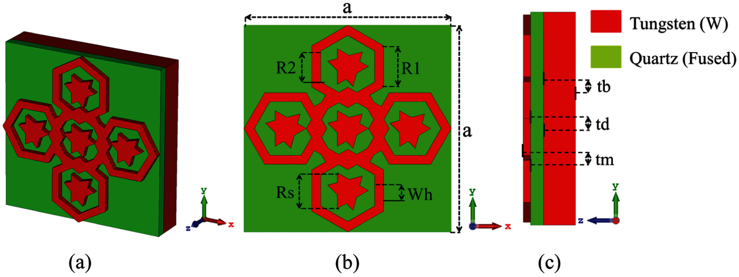
Figure 1: (a) Three-dimensional view of the unit cell, (b) Front view, and (c) Side view
2.3 Simulation Setup of Nano-Meta
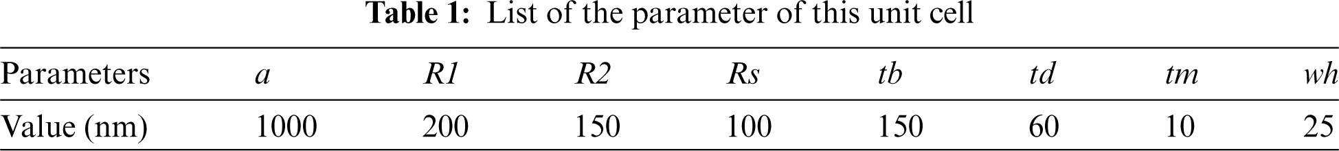
The numerical simulations are carried out by using terahertz mesh in frequency-domain solver based Computer Simulation Technology (CST Microwave Studio 2019) software. Fig. 2 shows the proposed MMA's boundary conditions, array configuration, and tetrahedral mesh properties. The positive and negative z-axis is used as a port position for transverse electromagnetic (TEM) propagation mode, as shown in Fig. 2a. Throughout the positive z-axis, the incident wave travels between the free space and met surface for impedance matching. Furthermore, for the TEM propagation mode, boundary conditions are set along the x and y-axis, where the positive z-axis is considered open-add-space boundary conditions. Meanwhile, perfect electric conductor (PEC) and perfect magnetic conductor (PMC) boundary conditions are set in the x-axis and y-axis, respectively. The perfect electric and magnetic conductor has been used to prevent the transmission of the proposed design. Polarization-independent electromagnetic response a schematic diagram of crossed trapezoid array. These symmetric 3 × 3 array configurations yield the same optical responses for TM and TE propagation mode which is shown in Fig. 2b. The unit cell boundary conditions of TE and TM mode are set along with the x and y-axis. Additionally, Fig. 2c shows the tetrahedral mesh properties where the maximum of five cells per model box edge is taken. Tetrahedral mesh with adaptive mesh refinement technique was adopted to perform the simulation. The scattering parameter in both ports becomes available for further reflection analysis and characterization during the electromagnetic wave propagation. The minimum and maximum edge lengths are 5.9427 nm and 176.343 nm, and this tetrahedral mesh analysis maintains a quality of 0.0300454 to 0.997996. “In total, 27821 number of tetrahedrons (the number of mesh cells) and keeps the average quality of 0.757251 (The average of all mesh cell quality values).
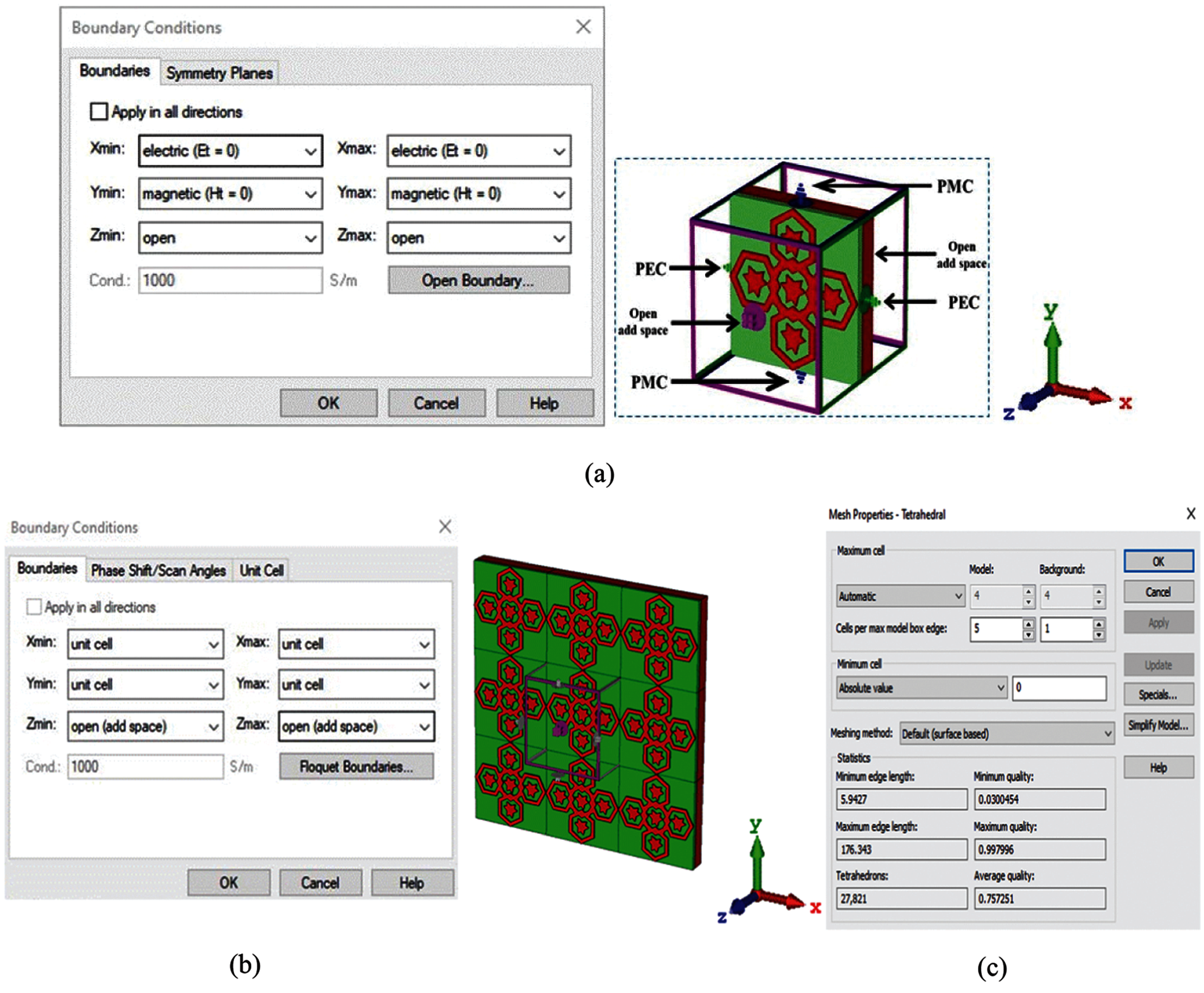
Figure 2: Boundary conditions setup (a) PEC and PMC boundary conditions for TEM mode (b) TE and TM mode (array configuration), and (c) Tetrahedral mesh properties
The proposed structure is compact with six hexagonal and six-star shapes Fig. 3a show the evaluation of the different shapes of the proposed unit cell. In addition, this study discusses the significant effect of circular and star shape loading in the center of six hexagonal. The transmission coefficient (S21) and absorbance of the proposed MMA unit cell is shown in Figs. 3b and 3c. Before adding any shape at the centre of the hexagonal shape, this structure is achieved −12 dB maximum magnitude and 93.68% peak absorption at the wavelength of 471.477 nm. Furthermore, this structure is completed average bandwidth of 25 nm between 460–485 nm. Meanwhile, the Hexagonal shape is loaded with five circular shapes. As a result, bandwidth is increased from 25 to 45 nm with a maximum magnitude of −33 dB. Moreover, this circular shape helps increase the peak absorption of 99.60% instant of 93.68% and is achieved an average absorption of 89% between 450 nm–501.77 nm. Adding a one-star shape increased its peak absorption from 93.68% to 95.12% at 475.78 nm. It also increases the bandwidth from 25 to 31 nm. In the stage of two-star shape loading, its maximum transmission coefficient S21 value is −22.72 dB in between 459.43–496 nm. Moreover, in this condition proposed structure is achieved a peak absorption of 99.90% at the wavelength of 473.76 and 54 nm bandwidth. After that, with the loading of another star shape, its transmission coefficient was −22.72 dB to −27.19dB. As a result, it increased its bandwidth from 54 nm to 78.8 nm and achieved peak absorption of 99.77%. In the cases of four-star shape loaded, its absorption is decreased dramatically. Still, its transmission coefficient value is increased −35.59 dB, and peak absorption is increased 99.99% at the wavelength of 471.09 nm. Finally, when five hexagonal shapes are loaded with the 5-star shapes, this structure achieves peak absorption of 99.90% at the wavelength of 466.60 nm and again increases its bandwidth from 51.71 nm to 81.62 nm. Finally, the proposed ZIM absorber structures demonstrate a wide bandwidth (450–600 nm) of visible wavelengths and exhibited almost perfect absorbance with 99.99% at the wavelength of 461.61 nm. Furthermore, the proposed structure is presented an average absorption of 0.8972 (89.72%) with polarization sensitivity and angle of incidence characteristics.
Figure 3: (a) Different shape of metamaterial design (b) Magnitude in dB scale (c) Absorbance
2.5 Methodology for Calculation of Absorbance
Maximum absorbance (A) of the proposed unit cell is conversely corresponding to the transmission
Here, Reflection,
The actual permittivity and permeability take out from the S parameters using Nicolson Ross Wire (NRW) [32]. Then, from the S parameters, achieve reflection, transmission magnitudes, and wave phase, respectively. Finally, manipulate the effective permittivity and permeability to perfect impedance matching and realized the perfect resonant in the free space. The unit cell characteristics impedance
Vacuum permittivity,
Vacuum permeability,
Relative permeability,
The reflection coefficient
Here,
3.1 Absorption Characteristics Investigations of the MMA
The tungsten has an extraordinary exhibition to impedance match in free space, and there is no surface plasmon of tungsten in optical wavelengths. The proposed MMA absorber is used tungsten as a resonator layer and the back layer. As seen, the value Z0 is barely lower than the value of Z (ω); this kind of absorber has to perform as an excellent potential super absorber. Incidents electromagnetic waves are controlled through the symmetrical structure. The back-layer metal plane wave incidents affected anticipate low transmission, and additional layers maintain the front-wave resonator and the dielectric layer. For low thickness characteristics, quartz (fused) supports to reduce the wavelength distance. Intrinsic losses characteristics of the front layer and the resonance characteristics of dielectric layers also help understand the impedance matching with the free space optical region. This singularity is caused by infiltration of the corresponding wave absorber of high performance and efficiency. Moreover, these wonders will display more excellent absorption if utilized the evenly organized hexagonal-shape resonator. The resonator appears the wave from the first stop as metal screens back layer wave once more consequently. The front layer comprises a metal resonator conjointly with a dielectric substrate (quartz), and the back layer is composed of a metal plane (tungsten). Fig. 4a illustrates the front layer subsidized greater to the absolute absorption while the back layer supports a complementary. In addition, this study observed that the front-layer absorption was reliable when back layer retention in the proposed structure. Fig. 4b is demonstrated the absorption, reflectance, and transmittance to the specified dimensions by tungsten and quartz (fused). The proposed design is exhibited perfect absorption of 0.9099 (99.99%) at 461.61 nm and an average absorption of 0.8972 (89.72%) between the wavelength of 450–600 nm. Light scattering in metamaterial absorbers decreases significantly from the UV to the near-IR. Recent studies employing near-IR transillumination and reflectance imaging, including optical coherence, indicate that this wavelength region is ideal for the high absorption polarization of materials. The opacity of developing metamaterial absorbers is essential in optimizing the contrast of polarization in reflectance measurements. It also influences proper EM wave propagation lesions in transillumination for TE mode compared to TM mode. Furthermore, light scattering in the absorber is more significant than in typical material; it is highly anisotropic and has a different spectral light scattering dependence. The objective of this study was to analyze the EM wave attenuation and absorption through absorbers at the optical range. Attenuation increased significantly with increasing wavelength, and the increases were not entirely consistent with increased EM wave absorption. Hence, the TE and TM mode PCR varies at the lower wavelength (∼ 460 nm).
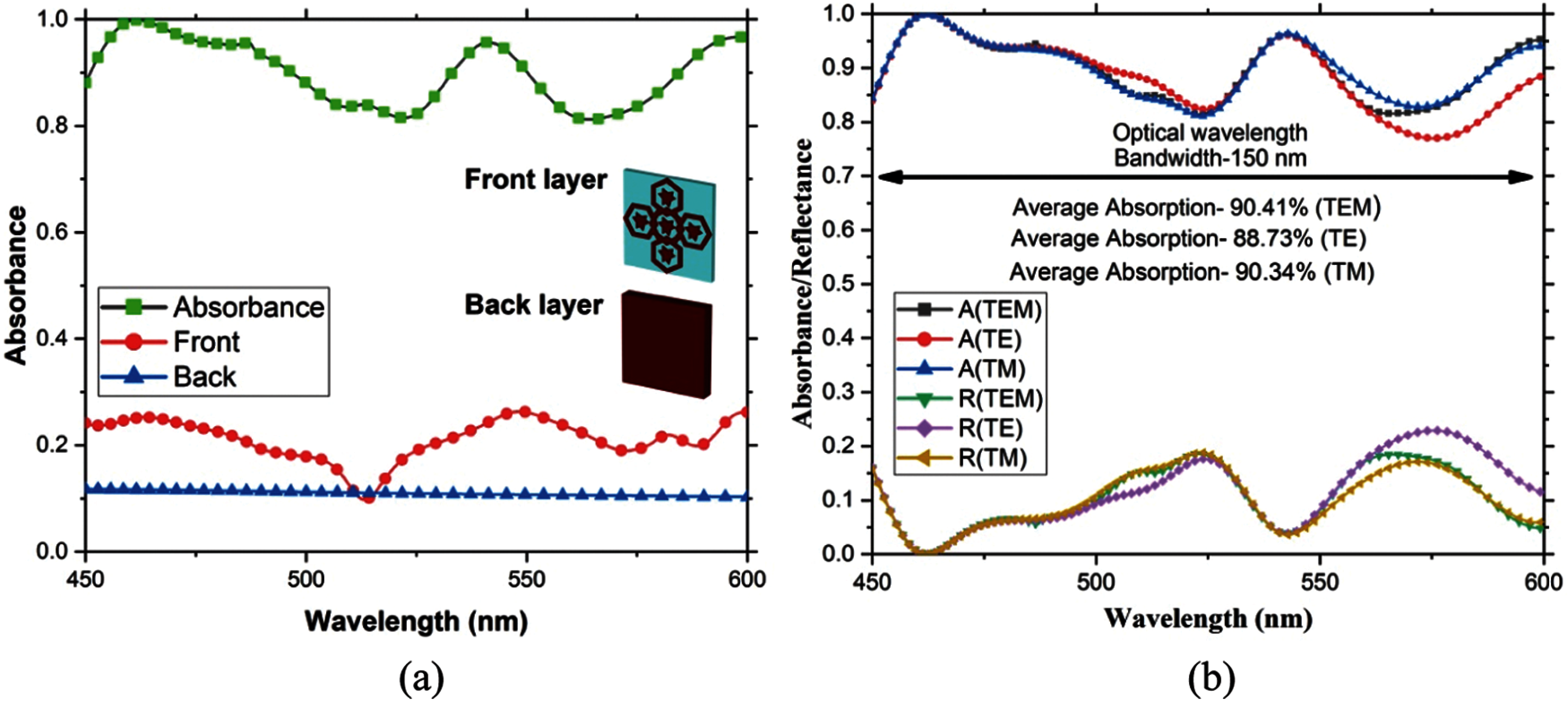
Figure 4: (a) Front and back-layer absorbance (b) Graphical representations of absorbance, reflectance, TE transmittance, and TM, TEM mode
3.2 Analysis Co-Polarization and Cross-Polarization Conversion Ratio (PCR) with MMA
The absorption curve of the proposed absorber is evaluated using Eq. (1) and Eq. (4). MMA unit cell cannot function as a polarized converter and provide PCR value instead of absorption. Co-polarization and cross-polarization conversion ratios are calculated with the help of S11, and S22 parameters show in Figs. 5a and 5b. The PCR indicates that the cross-polarization component is almost zero for the TM wave propagation mode on a linear magnitude scale. In a TE and TM mode of propagation near-zero, PCR value is observed different wavelength. Therefore, the unit cell should not function as a polarization converter and give a value of polarization conversion ratio (PCR) instead of absorbance [33].
The unit cell PCR can be calculated using Eq. (7) and Eq. (8) [33], as shown in Fig. 5a. The reflection coefficient (S11) of TE and TM mode is demonstrated in Fig. 5b.
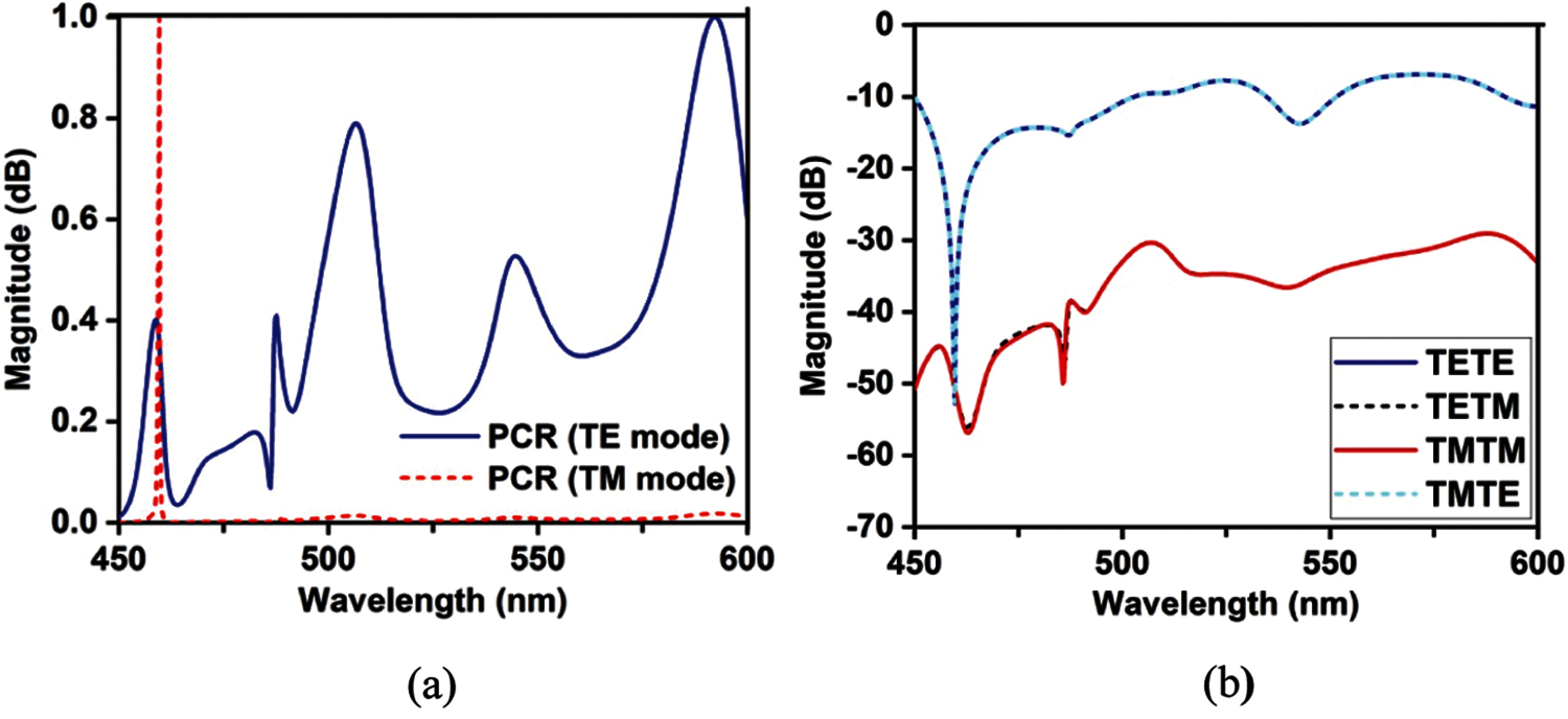
Figure 5: (a) PCR for both TE and TM mode of optical region (b) Reflection coefficient (S11) for TE and TM modes
3.3 Polarization and Incident Angle Stability of the Proposed MMA
The absorption of the proposed unit cell is calculated with different polarization and incidence angles at a transverse electromagnetic mode of propagation. The proposed design shows a wide-angle stable for both TE and TM modes. This study discusses the MMA performance with the various oblique incidences of TE and TM waves. The symmetrical structure of the MMA absorber is achieved entirely polarization-insensitive (0°–90°) shows in Figs. 6a and 6b.
The symmetrical structure can console such independent behavior angles of MMA with high absorption with suitable impedance matching. Besides, it can be used for optical sensors and does not need to change the sensor position with the position of the source's wavelength. The computational analysis is found 89.72% absorption on average, better than 32% with lossy semiconductor/metal potential as a solar energy harvester. However, perfect MMA must also be stable to the incidence angle before being used as a solar cell or energy harvesting, solar sensor, detector, and many other essential applications. Fig. 6c demonstrates the angular stability up to 45° for various incident angles at TE mode. Here, the unit cell changes the least, the average absorption at all incident angles is higher than 80%, and the peak absorption is 71%. Since the path length is proportional to the incidence angle, the greater the angle, the greater the path length. The confinement of waves in the dielectric layer is affected by this phenomenon and produces a lower absorption rate. For the TM mode, a different scenario occurred, shown in Fig. 6d instead of the TE mode we discussed above. Better stability and average absorption rate change from 90.1%–80.24% for incident angle 0°–45° this time. The proposed MMA absorption level does not change as much as the incident angle in TM mode. The larger electric field related to the normal incident angle rather than the parallel component is why the better stability in the TM mode. Excellent coupling and perfect wave confinement make this design an MMA with stable polarization and incident angle, thus enriching its application standards in many fields. The localized surface Plasmon (LSP) resonant has also been observed for TE and TM mode regarding the field interaction. LSP commonly seen as a confinement of surface plasmon inside a nanoparticle which have a comparable or small size with respect to light wavelength used for exciting the plasmon. The proposed structure have an asymmetric star inside each hexagonal loop with diagonal distance varying from 117.14 nm to 198.29 nm. The dimension is comparable to operating wavelength as the absorber numerically shows significant response at visible spectrum. Particularly at 458.54 nm the E-field and H-field shows a single resonance −34 dB and the remaining resonance points are not so dominant. The proposed structure vertical two hexagonal conducting part concentrate significant field and therefore contribute to LSP resonant.
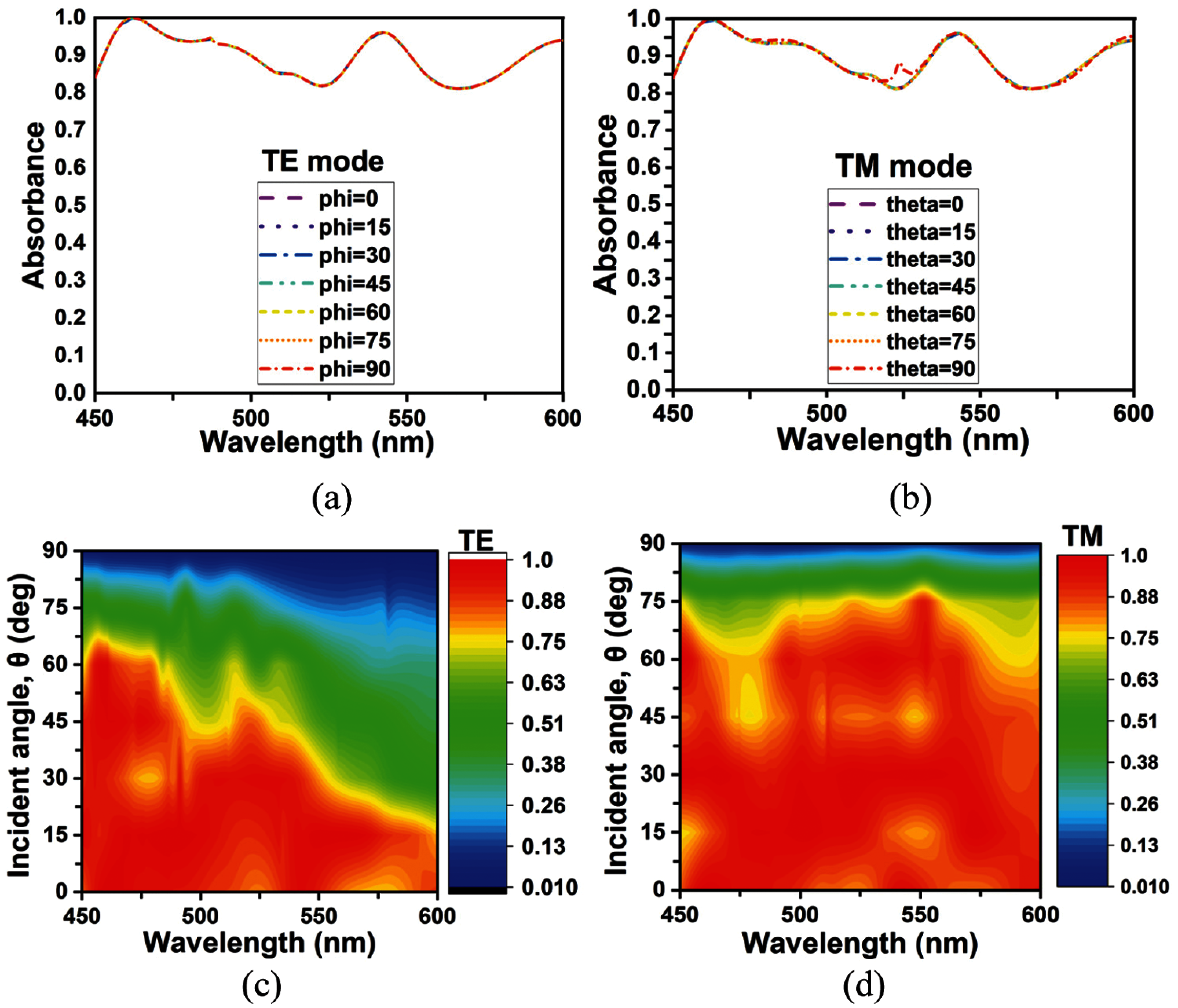
Figure 6: Absorption with different polarization angles at (a) TE mode (b) TM mode, (c) Absorption with different incident angle at TE mode (d) TM mode
3.4 Geometric Parameter Sweep of the MMA Unit Cell
The sweeping parameter helps determine the absorbance of the most excellent design and utilization. Sweeping the important parameter “R1,” the proposed hexagonal shape's external radius increases and decreases are observed. There are six hexagonal shapes presented in this design. The impact changing R1 parameter with an interval of 10 nm, hexagonal shape dimension also varies 180–220 nm shown in Fig. 7a. These changes include five steps and the adjusted difference between the hexagonal outer radius 10–40 nm. The extent of absorption of all values of the deviation from the hexagonal radius is greater than 90% identical, and at the resonance frequency, it gets 0.999 (99.99%) absorbance. The perfect absorbance finds at a radius of 40 nm, which seemed to be at R1 = 200 nm. Particular resonance wavelength shifts with the enhancements made to the outer radius “R1” of the hexagonal shape. Changing the second parameter, “R2,” the hexagonal shape's inner radius increased and decreased. In the middle of the absorption, the curve observed a minor up-down whenever it changed the particular parameter “R2” illustrated in Fig. 7b. The hexagonal inner dimension R2 varies from 130–170 nm at intervals of 10 nm. This specific alter included five steps and changes the contrast between the hexagonal internal sweep 10–40 nm. The resonance frequency varies insufficient but continuously stays up to 0.90 (90%). The absorption at the resonance frequency is 0.9999 (99.99%), and the magnitude of the absorption at operating wavelength 450–600 nm is more than 0.90 (90%).
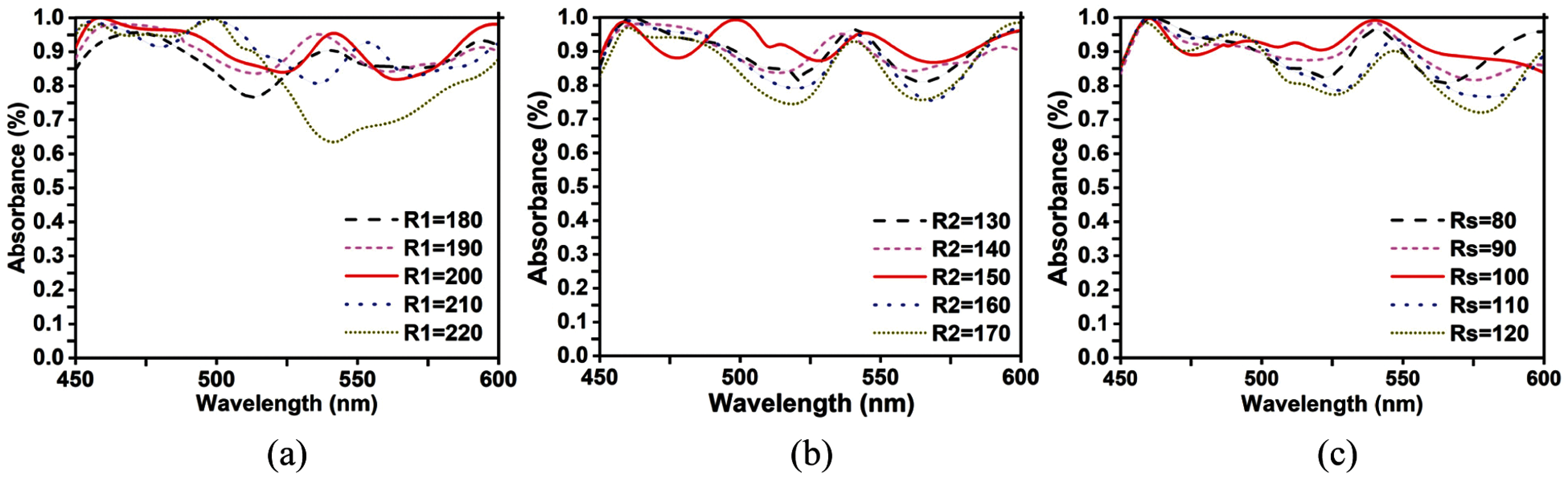
Figure 7: Wavelength response to a parameter sweep (a) Outer radius of hexagonal shape “R1”, (b) Inner radius of hexagonal shape “R2”, and (c) Radius of star shape “Rs.”
The perfect absorbance finds at the radius of R2 = 150 nm. Continuous increments of “R2” decreased the self-inductance but increased the typical inductance and the metal layer since the resonator shape expanded. These types of shared inductance developed the reverberation wavelength directly. These parametric types consider making a difference to all of us to decide the resonator's ideal measure. Varying the third parameter, “Rs” increased and decreased the star shape radius. Thus, the initial value slightly changes with the Rs value. Still, the end value is considerable up-down, shows in Fig. 7c. The impacts of star measurement Rs alter from 80–120 nm at an interval of 10 nm, and the perfect esteem was found at Rs = 100 nm. The resonance frequency varies insufficiently but remains permanently up to 0.90 (90%). Tab. 1 listed all the perfect parameters values of the propped unit cell.
3.5 Metamaterial Characterization of the Proposed Absorber
Metamaterial characterization refers to NRW [32] related to S11, and S21 expressed as complex relation in Eq. (9) where S0 = ± 1 and
where, Polarity of S0 changes and S11 remains unchanged. Polarization angle φ can change from +π to −π because of four (4) distinct polarity variations. In free space, both perpendicular and parallel polarization in basic waveguide mode (for example, TE10) shows a relationship between the square of wave vector
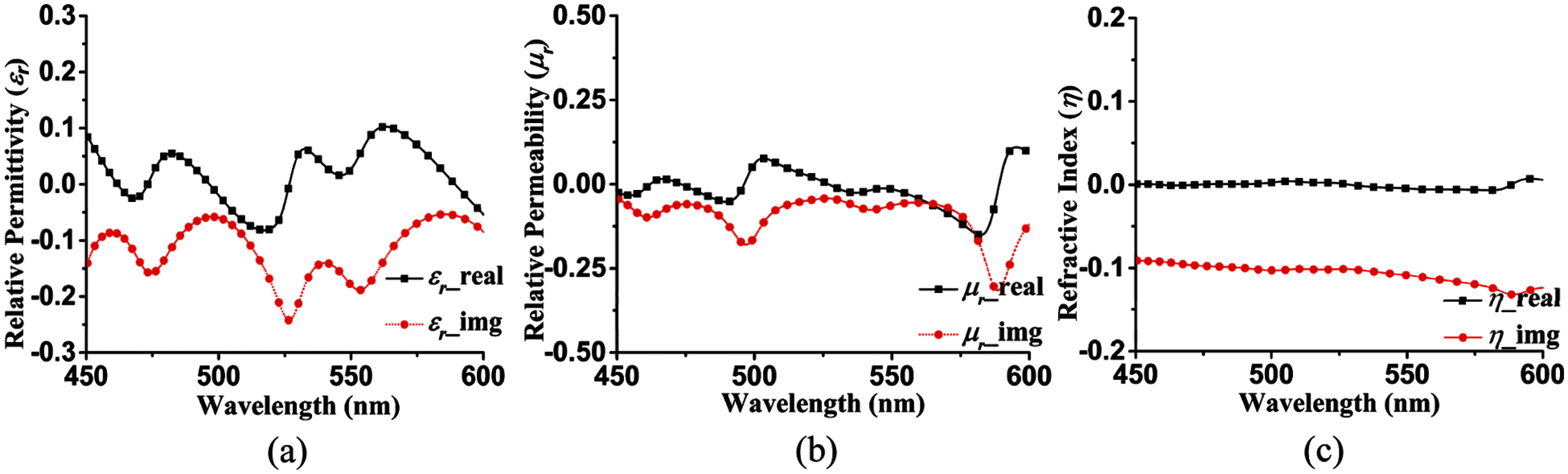
Figure 8: The dielectric properties characterization of the proposed MMA (a) Relative permittivity (b) Relative permeability (c) Refractive index
3.6 Electric Field, Magnetic Field, and Surface Current Analysis
The electromagnetic field and surface current distribution from 458.54 nm, 480 nm, and 540nm wavelength are presented in Fig. 9 to understand the proposed design's propagation energy. The electric field, magnetic field, and surface current distribution are shown in Figs. 9a–9c, respectively. Complete dissipation shown on the E-field at 458.54 nm resonance wavelength has the most significant absorbance with high resonator excitation. The magnetic field had an anti-parallel conveyance concerning the coupling impact of the resonator and metal. It appeared with exceptional appreciation at 458.54 nm but was energized mainly by the wavelength at each point. Fig. 9 seems the surface current conveyance, 480 nm, had a less strong surface current taken after by 458.54 nm, separately. Fig. 9c illustrated that surface current dispersion was exceptionally significant at 458.54 nm. Less energized in the back-layer was than the front-layer in all three phenomena.
3.7 Demonstrates the Simulated Data with CST and HFSS for Validation
The finite integration technique (FIT) based CST STUDIO SUITE® 2019 [35] software and finite element method based (FEM) based High-frequency simulation software package ANSYS HFSS 2017 is conducted to design, studies, and validates the performance of the proposed structure. Figs. 10a and 10b respectively present the S11 parameter and absorption of the proposed structure. The maximum absorption stays nearly equal at 0.9999 (99.99%), and the average absorption is above 0.8972 (89.72%) in the visible wavelength. Additionally, this study observes that the magnitude of the typically S11 parameter likewise synchronized quite well, which is an objective behind the match inside absorbance. The perfect absorption depends on the scatters (S11) parameter match very well in the operating spectrum. The back-layer has been made with tungsten, and the impedance coordinate with the free space, mainly the optical frequency, was the primary explanation behind this specific. Capacitive and inductive properties in the front layer from the resonator and lossless quartz (fused) were the cause for the absorption. Although overlooked silicon dioxide assimilation, that shows superb absorption consisting of a metal resonator. These design Comparisons with tungsten and quartz (fused) also simulated data verified by the finite element method (FEM) based high-frequency software (HFSS). However, there is a slight difference between the absorption curve and reflection coefficient because of the different methods is used in CST and HFSS software. Moreover, In CST software, we have used a reference plane, but in HFSS software didn't use any reference plane.
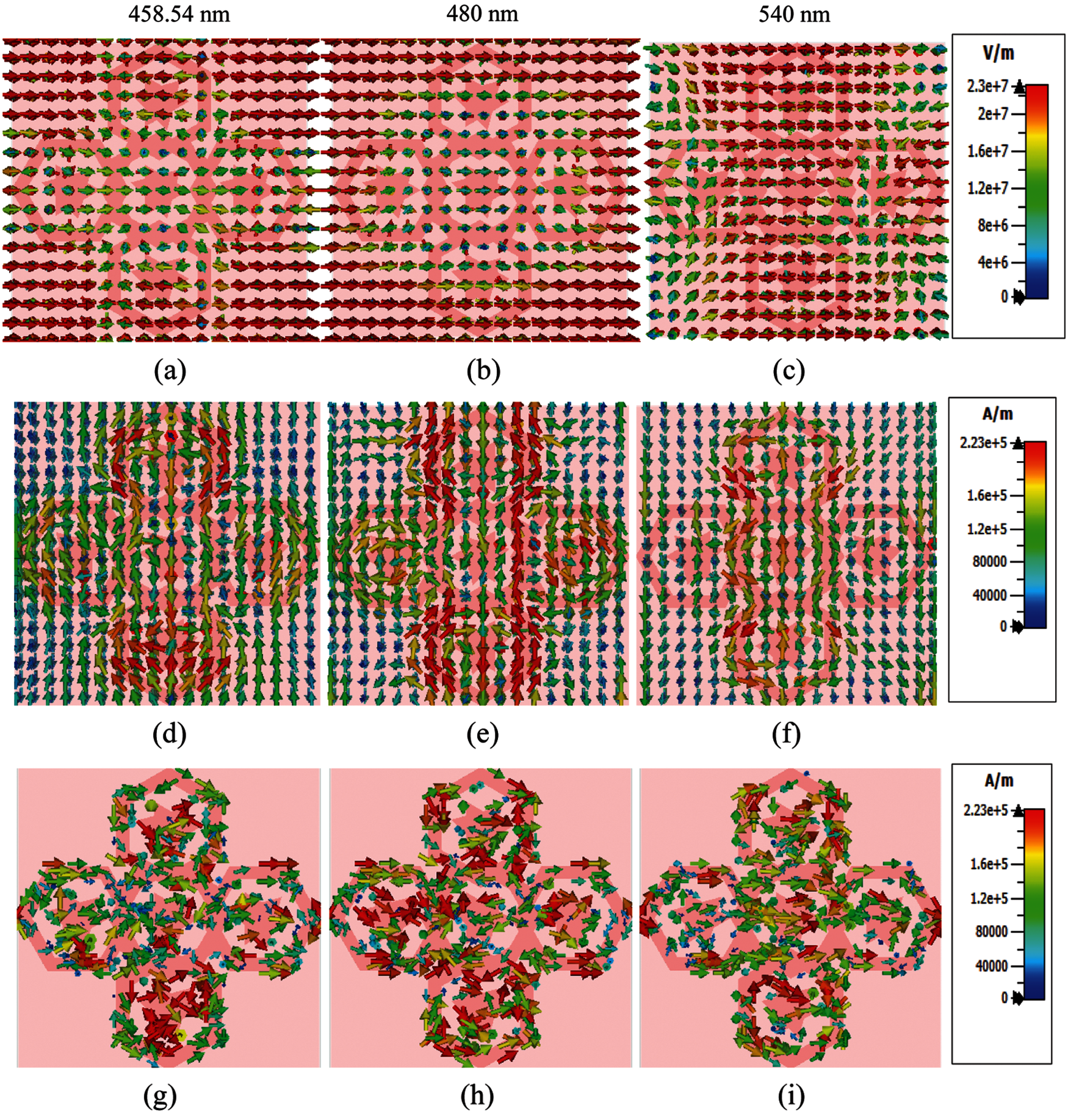
Figure 9: The E filed, H field and surfaced current at the wavelength of 458.54 nm, 480 nm, and 540 nm is presented in a, b, c; d, e, f; g, h, i, respectively
3.8 Aspect Ratio and Viability About Practical Fabrication
In general, aspect ratio refers to width to height dimension of any material structure. If the aspect ratio is high, then the structure has high possibility to maintain the pattern, thickness and molds of metal layer intact. The proposed structure aspect ratio is unity since the length and width is 1000 nm on both side. Due to thick ground layer of tungsten, creates a balanced front to back metal layer. Besides, the absorber structure likely to be suitable for ‘Microforming’ process. Microforming processes, also known as high aspect ratio micromachining (HARM) processes, use especially thick, patterned photoresist layers as molds for metal layers deposited via electroplating. In the LIGA microforming method, X-ray-based photoresist PMMA can be patterned in thick layers without worry of diffraction to create very high aspect ratio devices [36,37]. Another potential approach for nanofabrication is ‘Soft Lithography’ and ‘Nanoimprint Lithography’. Soft lithography basically a soft stamp that uses the method of microcontact printing (μCP) and nanoimprint lithography (NIL) and replica molding (REM) [36]. The basic concept is, first the master layer formed by the substrate material for example in the proposed structure it is Quartz (fused). Than elastomeric element used to create a soft mold for imprinting. So, all these fabrication process certify that the proposed nanoscale structure is feasible to fabricate.
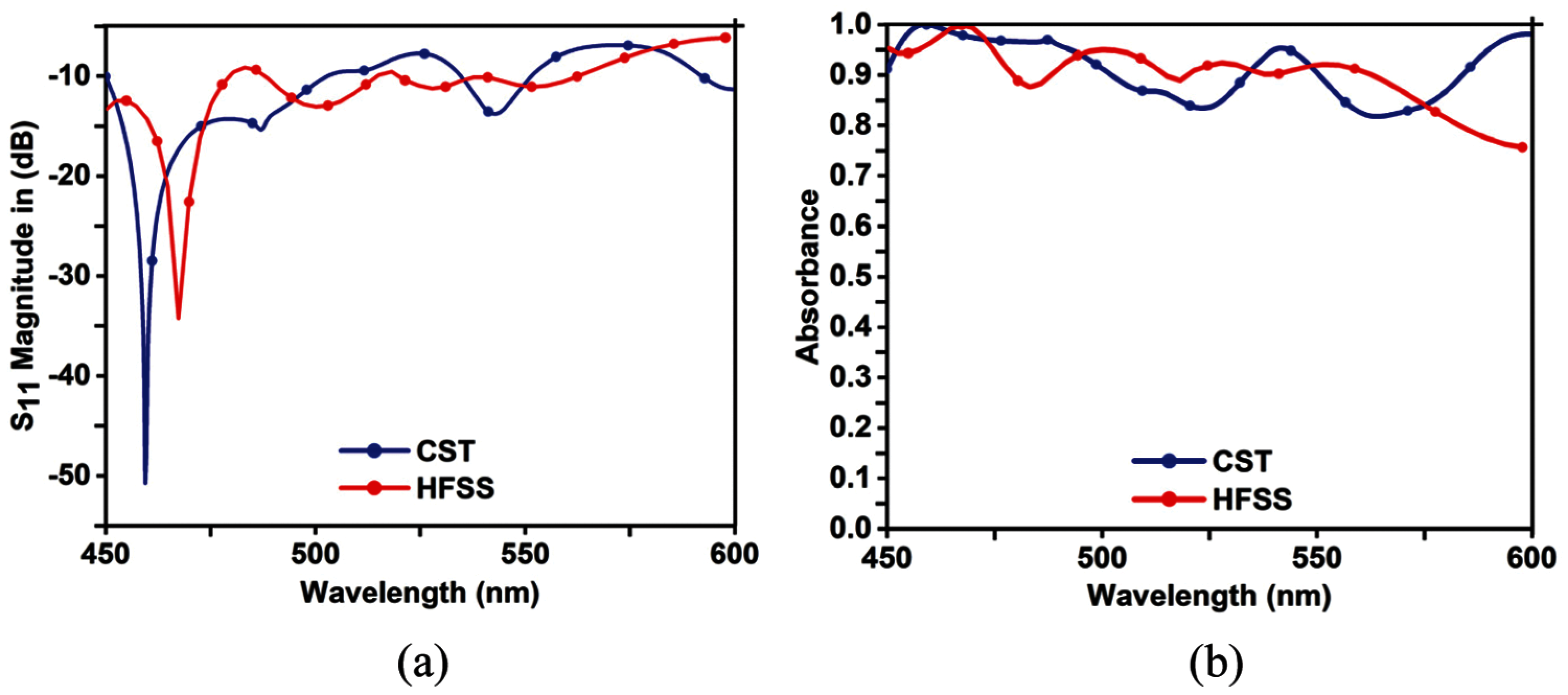
Figure 10: Comparison of different simulation methods (a) S11 parameter magnitude in dB (b) Absorption
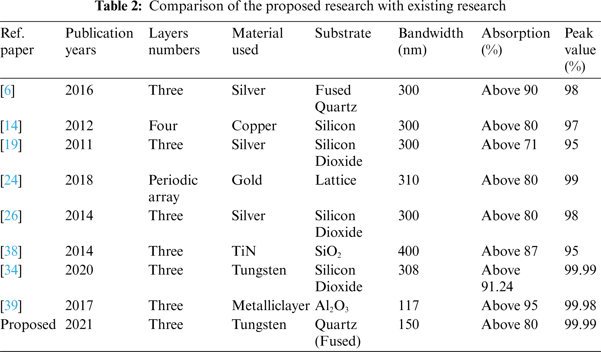
The proposed design is finding a remarkable absorption rate compared with the previous work. The evaluation of the proposed design and the previous work is demonstrated in Tab. 2. Culminate optical wavelength absorbers that could function in entire areas are once in a great exceedingly large area. A rare absorbance, almost perfect than 89.72% at all points with 99.99% peak points throughout optical wavelengths, is identified in the proposed design. A fantastic impedance organize of tungsten is perhaps the most reason for significant absorbance. This design utilizes a distinctive geometric structure compact with five hexagonal shapes, improving the property of absorption. The resonator and the back-layer metal are high with the equivalent capacitance. The exceptional softening level of tungsten and quartz (fused), effectiveness and operational area contrasted, and different materials utilized in Tab. 2 make this structure exclusive.
This paper reported a ZIM absorber based on tungsten and quart (fused). The proposed ZIM absorber structures demonstrate a wide bandwidth (450 nm–600 nm) of visible wavelengths and exhibited almost perfect absorbance with 99.99% at the wavelength of 461.61 nm and an average absorption of 89.72%. Furthermore, this structure is demonstrated polarization sensitivity and angle of incidence characteristic for both TE and TM modes. The symmetrical structure of the MMA absorber is achieved entirely polarization-insensitive (0°–90°). The proposed MMA has demonstrated angular stability up to 35° for various incident angles at TE mode. This absorption level does not change as much as the incident angle in TM mode. Due to the adaption of tungsten and lossless characteristics of quartz (fused), perfect absorption is taken out. Excellent coupling and perfect wave confinement make this design an MMA with stable polarization and incident angle, thus enriching its application standards in many fields. This ZIM absorber can be used as an optical sensor to shift the resonance and changes in the dielectric layer and the resonator thickness. A high combustion point of quartz (fused) would help to resist high temperatures naturally absorb. The exceptional combustion material has applied this study to achieved substantial absorbance, which may be effectively used in solar cells, optical sensors, color images, and thermal imaging applications.
Funding Statement: This work is supported by the Universiti Kebangsaan Malaysia research grant GUP-2020-074.
Conflicts of Interest: The authors declare that they have no conflicts of interest to report regarding the present study.
1. V. G. Veselago, “The electrodynamics of substances with simultaneously negative values of img align absmiddle alt ɛ eps/img and μ,” Physics-Uspekhi, vol. 10, no. 4, pp. 509–514, 1968. [Google Scholar]
2. D. R. Smith, W. J. Padilla, D. Vier, S. C. Nemat-Nasser, S. Schultz et al., “Composite medium with simultaneously negative permeability and permittivity,” Physical Review Letters, vol. 84, no. 18, pp. 4184, 2000. [Google Scholar]
3. D. Smith, D. Vier, T. Koschny and C. Soukoulis, “Electromagnetic parameter retrieval from inhomogeneous metamaterials,” Physical Review E, vol. 71, no. 3, pp. 036617, 2005. [Google Scholar]
4. F. Fan, X. Zhang, S. Li, D. Deng, N. Wang et al., “Terahertz transmission and sensing properties of microstructured PMMA tube waveguide,” Optics Express, vol. 23, no. 21, pp. 27204–27212, 2015. [Google Scholar]
5. S. S. Islam, M. R. I. Faruque and M. T. Islam, “A near zero refractive index metamaterial for electromagnetic invisibility cloaking operation,” Materials, vol. 8, no. 8, pp. 4790–4804, 2015. [Google Scholar]
6. X. Zhang, Y. Fan, L. Qi and H. Li, “Broadband plasmonic metamaterial absorber with fish-scale structure at visible frequencies,” Optical Materials Express, vol. 6, no. 7, pp. 2448–2457, 2016. [Google Scholar]
7. M. T. Islam, M. R. Islam, M. T. Islam, A. Hoque and M. Samsuzzaman, “Linear regression of sensitivity for meander line parasitic resonator based on ENG metamaterial in the application of sensing,” Journal of Materials Research and Technology, vol. 10, pp. 1103–1121, 2021. [Google Scholar]
8. E. Hoyer, W. Turner and N. Mokhov, “Absorbers for the high luminosity insertions of the LHC,” in Proc. of the 6th European Particle Accelerator Conf., Stockholm, Sweden, 1998: Citeseer. [Google Scholar]
9. C. M. Watts, X. Liu and W. J. Padilla, “Metamaterial electromagnetic wave absorbers,” Advanced Materials, vol. 24, no. 23, pp. OP181–OP181, 2012. [Google Scholar]
10. Y. Lee, P. Tuong, H. Zheng, J. Rhee and W. Jang, “An application of metamaterials: Perfect absorbers,” Journal of the Korean Physical Society, vol. 60, no. 8, pp. 1203–1206, 2012. [Google Scholar]
11. I. Hossain, M. Samsuzzaman, M. Singh, B. Bais and M. Islam, “Numerical investigation of polarization-insensitive multiband metamaterial for terahertz solar absorber,” Digest Journal of Nanomaterials and Biostructures, vol. 16, no. 2, pp. 593–600, 2021. [Google Scholar]
12. T. T. Nguyen and S. Lim, “Wide incidence angle-insensitive metamaterial absorber for both TE and TM polarization using eight-circular-sector,” Scientific Reports, vol. 7, no. 1, pp. 1–11, 2017. [Google Scholar]
13. Y. Zhang, T. Li, Q. Chen, H. Zhang, J. F. O'Hara et al., “Independently tunable dual-band perfect absorber based on graphene at mid-infrared frequencies,” Scientific Reports, vol. 5, pp. 18463, 2015. [Google Scholar]
14. P. Zhu and L. Jay Guo, “High performance broadband absorber in the visible band by engineered dispersion and geometry of a metal-dielectric-metal stack,” Applied Physics Letters, vol. 101, no. 24, pp. 241116, 2012. [Google Scholar]
15. X. Duan, S. Chen, W. Liu, H. Cheng, Z. Li et al., “Polarization-insensitive and wide-angle broadband nearly perfect absorber by tunable planar metamaterials in the visible regime,” Journal of Optics, vol. 16, no. 12, pp. 125107, 2014. [Google Scholar]
16. P. Rufangura and C. Sabah, “Dual-band perfect metamaterial absorber for solar cell applications,” Vacuum, vol. 120, pp. 68–74, 2015. [Google Scholar]
17. A. K. Azad, W. J. Kort-Kamp, M. Sykora, N. R. Weisse-Bernstein, T. S. Luk et al., “Metasurface broadband solar absorber,” Scientific Reports, vol. 6, pp. 20347, 2016. [Google Scholar]
18. M. Heidari and S. Sedighy, “Broadband wide-angle polarization-insensitive metasurface solar absorber,” JOSA a, vol. 35, no. 4, pp. 522–525, 2018. [Google Scholar]
19. K. Aydin, V. E. Ferry, R. M. Briggs and H. A. Atwater, “Broadband polarization-independent resonant light absorption using ultrathin plasmonic super absorbers,” Nature Communications, vol. 2, no. 1, pp. 1–7, 2011. [Google Scholar]
20. C. Wang, S. Yu, W. Chen and C. Sun, “Highly efficient light-trapping structure design inspired by natural evolution,” Scientific Reports, vol. 3, no. 1, pp. 1–8, 2013. [Google Scholar]
21. M. Otomori, T. Yamada, K. Izui, S. Nishiwaki and N. Kogiso, “Level set-based topology optimization for the design of light-trapping structures,” IEEE Transactions on Magnetics, vol. 50, no. 2, pp. 729–732, 2014. [Google Scholar]
22. C. Li, H. Fan, Q. Dai, Z. Wei, S. Lan et al., “Multipole resonance in arrays of diamond dielectric: A metamaterial perfect absorber in the visible regime,” Nanomaterials, vol. 9, no. 9, pp. 1222, 2019. [Google Scholar]
23. A. D. Khan, A. D. Khan, S. D. Khan and M. Noman, “Light absorption enhancement in tri-layered composite metasurface absorber for solar cell applications,” Optical Materials, vol. 84, pp. 195–198, 2018. [Google Scholar]
24. N. T. Q. Hoa, P. D. Tung, P. H. Lam, N. D. Dung and N. H. Quang, “Numerical study of an ultrabroadband, wide-angle, polarization-insensitivity metamaterial absorber in the visible region,” Journal of Electronic Materials, vol. 47, no. 5, pp. 2634–2639, 2018. [Google Scholar]
25. Y. I. Abdulkarim, L. Deng, F. F. Muhammad and L. He, “Enhanced light absorption in the organic thin films by coating cross-shaped metamaterial resonators onto the active layers,” Results in Physics, vol. 13, pp. 102338, 2019. [Google Scholar]
26. S. Butun and K. Aydin, “Structurally tunable resonant absorption bands in ultrathin broadband plasmonic absorbers,” Optics Express, vol. 22, no. 16, pp. 19457–19468, 2014. [Google Scholar]
27. Y. Qi, Y. Zhang, C. Liu, T. Zhang, B. Zhang et al., “A tunable terahertz metamaterial absorber composed of hourglass-shaped graphene arrays,” Nanomaterials, vol. 10, no. 3, pp. 533, 2020. [Google Scholar]
28. I. Hossain, M. Samsuzzaman, M. Moniruzzaman, B. B. Bais, M. S. J. Sing et al., “Polarization-independent broadband optical tegime metamaterial absorber for solar harvesting: A numerical approach,” Chinese Journal of Physics, vol. 71, pp. 699–715, 2021. [Google Scholar]
29. G. Ghosh, “Dispersion-equation coefficients for the refractive index and birefringence of calcite and quartz crystals,” Optics Communications, vol. 163, no. 1–3, pp. 95–102, 1999. [Google Scholar]
30. P. M. Schneider and W. B. Fowler, “Band structure and optical properties of silicon dioxide,” Physical Review Letters, vol. 36, no. 8, pp. 425, 1976. [Google Scholar]
31. H. Tao, N. I. Landy, C. M. Bingham, X. Zhang, R. D. Averitt et al., “A metamaterial absorber for the terahertz regime: Design, fabrication and characterization,” Optics Express, vol. 16, no. 10, pp. 7181–7188, 2008. [Google Scholar]
32. E. J. Rothwell, J. L. Frasch, S. M. Ellison, P. Chahal and R. O. Ouedraogo, “Analysis of the nicolson-ross-weir method for characterizing the electromagnetic properties of engineered materials,” Progress in Electromagnetics Research, vol. 157, pp. 31–47, 2016. [Google Scholar]
33. C. X. Huang, J. J. Zhang, L. Wu, C. Zhang, J. Yang et al., “Multi-band tunable chiral metamaterial for asymmetric transmission and absorption of linearly polarized electromagnetic waves,” Advanced Theory and Simulations, vol. 3, no. 12, pp. 2000179, 2020. [Google Scholar]
34. S. Mahmud, S. S. Islam, K. Mat, M. E. Chowdhury, H. Rmili et al., “Design and parametric analysis of a wide-angle polarization-insensitive metamaterial absorber with a star shape resonator for optical wavelength applications,” Results in Physics, vol. 18, pp. 103259, 2020. [Google Scholar]
35. M. Moniruzzaman, M. T. Islam, G. Muhammad, M. S. J. Singh and M. Samsuzzaman, “Quad band metamaterial absorber based on asymmetric circular split ring resonator for multiband microwave applications,” Results in Physics, vol. 19, pp. 103467, 2020. [Google Scholar]
36. S. A. Campbell, Fabrication engineering at the micro-and nanoscale (no i9780195320176). 2008. [Google Scholar]
37. P. Rai-Choudhury, In Handbook of Microlithography, Micromachining, and Microfabrication: Microlithography, SPIE press, USA, 1997. [Google Scholar]
38. W. Li, U. Guler, N. Kinsey, G. V. Naik, A. Boltasseva et al., “Refractory plasmonics with titanium nitride: Broadband metamaterial absorber,” Advanced Materials, vol. 26, no. 47, pp. 7959–7965, 2014. [Google Scholar]
39. P. Liu and T. Lan, “Wide-angle, polarization-insensitive, and broadband metamaterial absorber based on multilayered metal–dielectric structures,” Applied Optics, vol. 56, no. 14, pp. 4201–4205, 2017. [Google Scholar]
 | This work is licensed under a Creative Commons Attribution 4.0 International License, which permits unrestricted use, distribution, and reproduction in any medium, provided the original work is properly cited. |