DOI:10.32604/cmc.2022.019789
| Computers, Materials & Continua DOI:10.32604/cmc.2022.019789 | |
| Article |
Efficient Energy Optimized Faithful Adder with Parallel Carry Generation
1Dr. Mahalingam College of Engineering and Technology, Pollachi, Tamilnadu, India
2Dhirajlal Gandhi College of Technology, Salem, Tamilnadu, India
*Corresponding Author: S. Maragatharaj. Email: maragatharaj.ece@dgct.ac.in
Received: 25 April 2021; Accepted: 04 June 2021
Abstract: Approximate computing has received significant attention in the design of portable CMOS hardware for error-tolerant applications. This work proposes an approximate adder that to optimize area delay and achieve energy efficiency using Parallel Carry (PC) generation logic. For ‘n’ bits in input, the proposed algorithm use approximate addition for least n/2 significant bits and exact addition for most n/2 significant bits. A simple OR logic with no carry propagation is used to implement the approximate part. In the exact part, addition is performed using 4-bit adder blocks that implement PC at block level to reduce node capacitance in the critical path. Evaluations reveal that the maximum error of the proposed adder confines not more than 2n/2. As an enhancement of the proposed algorithm, we use the Error Recovery (ER) module to reduce the average error. Synthesis results of Proposed-PC (P-PC) and Proposed-PCER (P-PCER) adders with n-16 in 180nm Application Specific Integrated Circuit (ASIC) PDK technology revealed 44.2% & 41.7% PDP reductions and 43.4% & 40.7% ADP reductions, respectively compared to the latest best approximate design compared. The functional and driving effectiveness of proposed adders are examined through digital image processing applications.
Keywords: Application-specific integrated circuit; approximate computing; power dissipation; energy dissipation; image processing
Full adder (FA) is a vital component of processing elements used in multimedia computing, digital signal processing and digital image processing systems. The bit-width of the arithmetic units depends on the processing capability of digital systems. As the bit width in adders increase, the delay associated with carry propagation also increases linearly-O (n), where ‘n’ is the length of input bits [1]. Diverse topologies of adders such as Carry Select Adder (CSLA) [1], Carry Skip Adder (CSKA) [2], Carry Propagate Adder(CPA) [3], Carry Look Ahead Adder(CLA) [1] are proposed to moderate carry propagation delay at the expense of area overhead. Area efficient CSLA with gate-level Binary to Excess one Conversion (BEC) circuit is proposed in [4]. CLA achieves significantly less delay (O (log(n)) at the expense of gate area (O(n log(n))) [5,6].
Parallel adders offer a reliable alternative to conventional adders for high-speed applications. Aggressive scaling in deep submicron technologies and demand for faster compact ICs have put the onus on adders to be structurally optimized. The nature of multimedia signals and image processing applications involving human perception provides the opportunity to exploit the limited range of resources at the expense of certain errors in processed outputs [7,8]. Approximate computing is a novel technique to design low power, reduced hardware architecture for the above mentioned error-tolerant applications [9–13].
Initial works on approximate adders were implemented in the form of speculative adders [14]. Speculative adders use a control signal to decide the choice among input bits in approximate and accurate logic in multi-bit addition. Segmented adders to reduce the propagation of error signals were put forth in [15]. Approximate designs for addition viz., ET-CSLA [16], SAET-CSLA [16], HPETA [17], SARA [18] and area-efficient parallel adder (AEPA) [19] are proposed in literature. ET-CSLA [16] use approximate 1-bit FA cell for all bits in input operands and hence exhibit significant area saving at the cost of high error. For 16-bit addition, SAET-CSLA [16] uses conventional CSLA for the most significant 8 bits and ET-CSLA [16] for the least significant 8 bits (inaccurate part). The hybrid design demonstrates better accuracy compared to ET-CSLA [16]. Reference [17] proposed two variants of high-performance error-tolerant adders (HPETAs) for image processing applications. Reference [18] proposed a multi-bit adder that segregates input bits into sub-groups, and approximate/exact carry-in for each sub-block is configured. Though the design in Reference [18] uses a look-ahead based approach for carry generation, it reduces area overhead significantly compared to conventional carry look-ahead adder. Reference [19] proposed Area Efficient Parallel Adder (AEPA) using new error-tolerant FA cells in approximate part that limits the maximal error within bound. Simulations revealed that the area of AEPA is significantly high compared to approximate adders in [18].
In this brief, we propose a high-speed area efficient approximate adder that performs multi-bit addition in block sets, with parallel carry generation logic implemented at block level in the accurate part and simple OR logic on the least significant n/2 bits(approximate part). Evaluations revealed that the maximal error in the proposed adder, due to approximation, confines to 2n/2. The rest of the paper is organized as follows. Section 2 presents the area and delay evaluation of various adder algorithms. Section 3 presents the design methodology of proposed adders. Next, Section 4 evaluates the performance of the proposed adders. Furthermore, Section 5 discusses the implementations of the proposed adders in digital image processing applications. Finally, Section 6 gives a brief conclusion on the proposed work.
2 Area and Delay Evaluation of Adder Algorithms
The SOP implementation of combinational functions employs AOI (AND-OR-INVERT) logic for CMOS realization. AOI structure for Sum and Carry outputs of a conventional 1-bit Full Adder (FA) cell is shown in Fig. 1. The gates in same row within dotted lines perform a parallel operation, and hence we consider one gate delay for parallel gates. Area cost is evaluated by the total count of AOI gates used in the logic design. From Fig. 1, the logic delay and gate count (GC) of 1 bit FA are given by (1) & (2), respectively.
where ‘+’ represents arithmetic OR operation. Based on the above methodology, we have evaluated various adders' critical delay and area and discussed them in the following subsections.
In CMOS realization RCA [1] offers better structural regularity due to the series arrangement of FA cells. An n bit RCA is constructed using n FA cells cascaded together, with the carryout bit of one FA tied to the carry-in bit of the next higher weight FA cell. However, RCA incurs high carry propagation delay due to rippling of carry signal from least significant bit position to the most. Critical delay of n-bit RCA (tRCA) is given by (3).
where tFA is the carry generation delay of 1 bit FA cell. From (3), it is evident that the delay of n bit RCA depends on tFA and it increases in O (n). Hence, minimizing tFA of 1bit FA cell will minimize tRCA. From Fig. 1, GC of n-bit RCA is given by
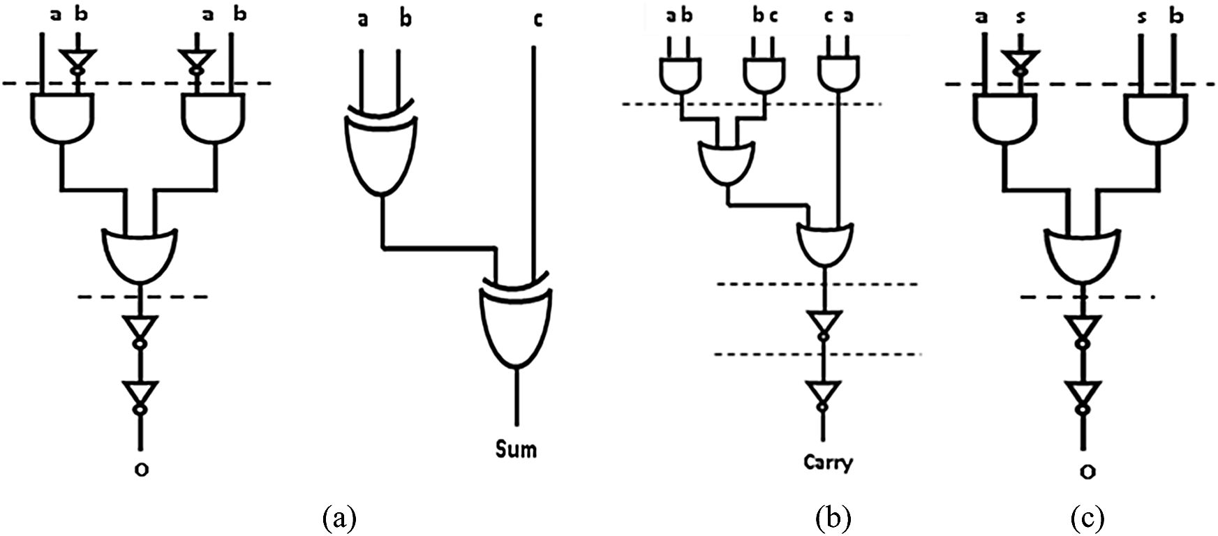
Figure 1: AOI implementation of a) 1 bit FA sum, b) 1 bit FA carry, c) 2:1 mux
CSLA [1] performs high-speed addition using an array of RCA pair and 2:1 Muxes. Each RCA block performs addition independently with carry-in as either logic low or logic high. For n = 16, with 4 bits in an RCA block, the CSLA design will have 4 RCA pairs. MUX units use the Carryout (Cout) signal from preceding blocks to produce final output from Sum signals generated by the RCA pair at the corresponding binary weight. Fig. 2 shows the block level architecture for n bit CSLA.
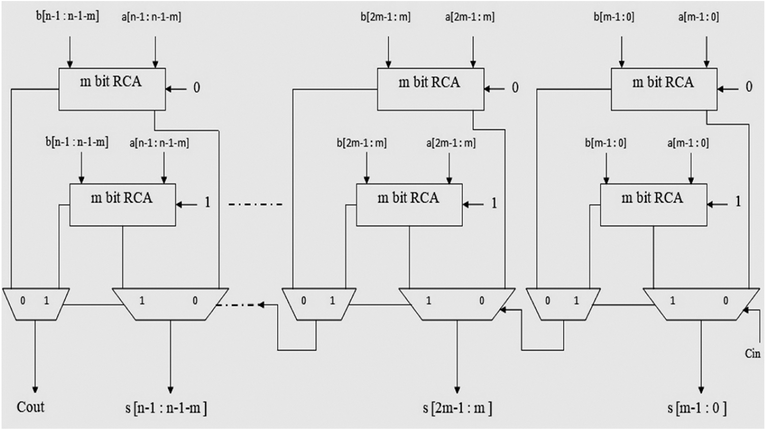
Figure 2: Block diagram of n bit CSLA
If the carry propagation time of 1bit FA and propagation delay of Mux units are represented as tFA and tmux respectively, then delay of n bit CSLA design with m Fas in a block is given by (5)
From Fig. 2, the gate count of n-bit CSLA is given by
CLA [5,6] eliminates the carry-rippling problem encountered in RCA by generating carry signals at corresponding binary weights using Cin and Propagate (P), Generate (G) signals generated at lower weights. Hence the area cost and hardware complexity of CLA are high for large input bit widths compared to RCA. Following are the functional symbols used to express logic functions viz., |−OR; ∗−AND; ∩−XOR. Based on the above representation, the logic expression for Carry signal (Ci) is given by
where,
Using (7), critical delay of n-bit CLA (tCLA) is given by
Based on AOI representation in Fig. 1, GC of n-bit CLA is given by
Tab. 1 compares the logic depth and area of the various adders discussed in subsections Figs. 2a–2c, assuming delay and area of each gate to be 1 unit. Note from Tab. 1, RCA performs better in terms of area saving while CSLA performs better in speed improvement. CLA can optimize area and delay significantly.
However, CLA exhibits high hardware complexity and insufficient regularity of cell arrangement compared to RCA for large n, making it unsuitable for CMOS realization. Limiting the number of bits in CLA improves the regularity of structure and reduces hardware complexity. Hence, in the proposed approach input bits are grouped into four, and PC logic-based addition is performed within the group in the accurate part. Furthermore, the approximate part of the adder is implemented with simple OR logic to reduce area and delay.
This section briefs the proposed approximate adders that implement carry-free addition in the least significant approximate part (n/2 bits) and error-free addition in the most significant part. Accurate part of the adder is implemented with a hybrid approach that combines block-level addition with look ahead based fast parallel carry generation. Fig. 3 shows the block-level architecture of the proposed adder.
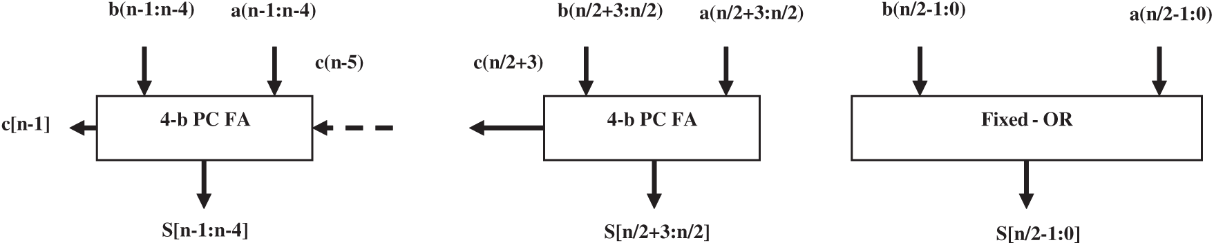
Figure 3: Block diagram of proposed adder
In the proposed addition algorithm, for n bits in input operands and 4 bits in a block, the number of blocks in the exact part will be n/8. It is noted from (9), Ci is a combination Primary Carry Propagate (PCP) term that propagates input carry-Cin and Intermediate Carry Propagate (ICP) term that propagates in-between carry signals generated at lower significant bit positions. PCP and ICP are defined by (10) & (11), respectively.
Analysis of (10) & (11) reveals that parallelism can be exploited at two levels viz., (i) within ICP by merging consecutive odd and even terms, (ii) between ICP and PCP by generating PCP AND terms in parallel with level-1 logic reduction in ICP. Generation of carry signals using proposed delay balanced carry look ahead algorithm for 4-bit addition is shown in (12)–(15), and the corresponding gate level diagram is shown in Fig. 4.
Note from Fig. 4, ICP use certain PCP AND terms generated in level-1 logic reduction in further stages and this in turn reduces the gate count and delay significantly. From Fig. 4, the logic delay of Cin to C1–C4 (tc) is given by
Also, it is noted from Fig. 4 that delay balanced PC logic maintains uniform gate delay from Cin to carry out signals in the accurate part. Furthermore, it is observed that Cin is used as an input in the pre-final stage and hence provides a choice for further delay reduction in subsequent higher weight adder blocks. Evaluations revealed that the Proposed PC (P-PC) adder incurs n/8 * tc logic delay while conventional RCA implementation of accurate part incurs n/2(tc) logic delay. Hence, delay balanced PC logic in the proposed adder demonstrates 83.3% logic depth reduction compared to the standard implementation. In the least significant approximate part of the P-PC adder, carry signals are not generated, and sum signals are generated using approximate full adder (AFA) cells. Boolean expression that defines the logic of AFA cell is given by (17).
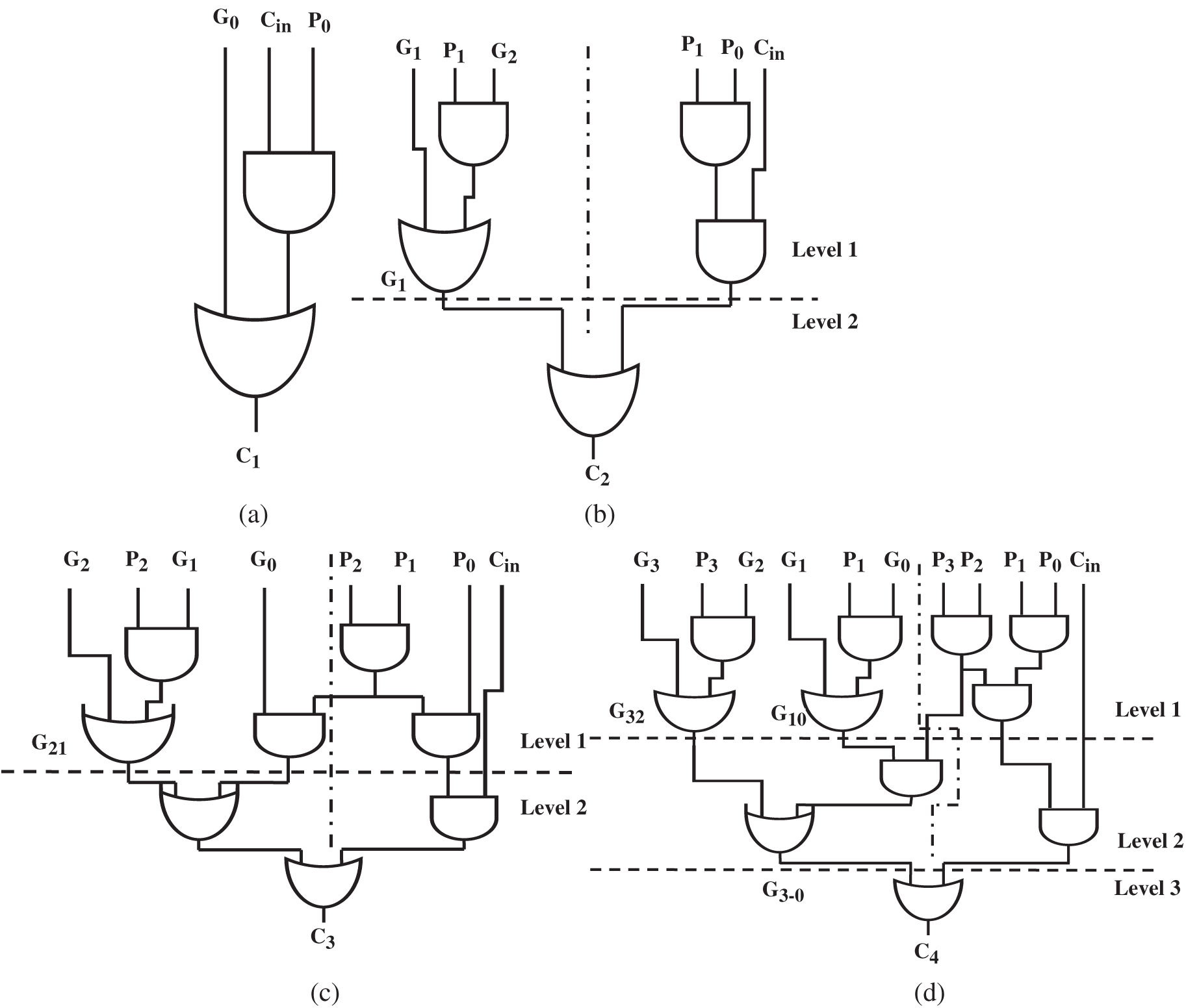
Figure 4: Gate level diagram of Carry generation using PC logic for n − 4
Note from (10) AFA in the approximate part generates an error for input a = b = logic high. However, approximate sum = 1 for a = b = 1, which reduces the mean error distance (MED) due to the elimination of carry signal to 1 at the corresponding binary weight. Hence, the proposed approximation logic reduces delay and average error significantly. Evaluations reveal that the maximum error due to approximation in P-PC adder is not more than 1unit at bit position n/2 (UBP-n/2).
The novelty of the proposed design is that it trades-off error for penalty in area overhead, and this can be realized using an error recovery unit. In proposed design 2 (P-PCER), the algorithm generates an error recovery (ER) signal using Generate (G) and approximate sum signals and is added to the exact part of adder at least significant bit position. Boolean expression defining logic of ER is given by (18).
where ‘j’ represents the count of most significant bits in the approximate part considered for ER signal generation. Note that, ER signal reduces the maximum error (ME) in the proposed adder to 2n/2 − 1 with probability P(ME) = 2i/n and mean error significantly. Fig. 5 shows the block level architecture of the P-PCER design.
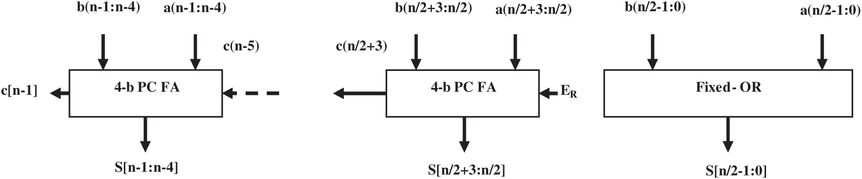
Figure 5: Block diagram of P-PCER adder
Error metrics are the essential parameters to evaluate the efficiency of an approximate design in error-tolerant applications. In this section, performance of the proposed approximate adders and state-of-the-art approximate designs is evaluated in terms of various error metrics [19,20] using standard output as the reference. The accuracy metrics considered are: Mean Error Distance (MED), Mean Relative Error Distance (MRED), Normalized Error Distance (NED) and Percentage Accuracy defined as follows.
where, EDi-Error Distance at output combination corresponding to ith input combination, Si-exact output corresponding to ith combination, D-maximum possible ED of an approximate circuit and Re-exact result.
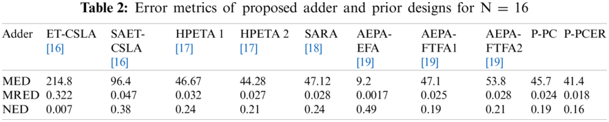
Tab. 2 compares MED, MRED and NED value of the proposed and prior adder designs. Note from Tab. 2, that proposed adders fares better MED and MRED values compared to ET-CSLA [16], SAET-CSLA [16], HPETA1 [17], HPETA2 [17], SARA [18], AEPA-FTFA1 [19] and AEPA-FTFA2 [19] designs. AEPA-EFA [19] design use exact full adder cell in approximate and accurate part. Hence MED, MRED and NED values of AEPA-EFA [19] design are significantly better compared to proposed and state-of the art adder designs. P-PCER design fare better in MED, MRED and NED values compared to the P-PC design, thanks to the error recovery unit used in P-PCER design.
4.2 Area, Delay and Power Comparison
Performance of the proposed and state-of the art adders in terms of total power dissipation (power), area, delay, Area-Delay Product (ADP), Power-Delay Product (PDP) and Energy-Delay Product (EDP) are shown in Tab. 3. Note from Tab. 3, P-PC and P-PCER adders demonstrates 30.8% & 28.8%; 35.9% & 34%; 54.7% & 53.4%; 45.5% & 43.8%; 44.7% & 43.1%; 40.3% & 38.5%;58.8% & 57.6%;47.2% & 45.6% and 42.1% & 40.4% power reductions compared to conventional CLA [1], ET-CSLA [16], SAET-CSLA [16], HPETA1 [17], HPETA2 [17], SARA [18], AEPA-EFA [19], AEPA-FTFA1 [19] and AEPA-FTFA2 [19] designs respectively. Though SARA [18] implement look ahead based carry propagation in the accurate part, it shows 11.2% and 9.8% high delay compared to P-PC and P-PCER adders, thanks to the parallel carry generation logic that reduce delay of the proposed designs significantly. ET-CSLA [16], SAET-CSLA [16], HPETA1 [17], HPETA2 [17], AEPA-EFA [19], AEPA-FTFA1 [19] and AEPA-FTFA2 [19] adders use carry select algorithm and hence delay of these adders depends on the number of FA cells in a block and increases in the order of number of blocks and 2:1 Mux delay. In terms of PDP, P-PC and P-PCER adders demonstrates 50.8% & 48.5%; 35.7% & 32%; 57.3% & 55.3%; 49.3% & 46.9%; 48.9% & 46.6%; 47% & 44.5%; 68.1% & 66.6%; 49.5% & 47.2% and 44.2% & 41.7% reductions compared to conventional CLA [1], ET-CSLA [16], SAET-CSLA [16], HPETA1 [17], HPETA2 [17],SARA [18], AEPA-EFA [19], AEPA-FTFA1 [19] and AEPA-FTFA2 [19] adders respectively.
Also note from Tab. 3, P-PC and P-PCER adders show 34.5% & 32.4%; 41.1% & 39.2%; 58.3% & 56.8%; 47.4% & 45.9%; 48.2% & 46.5%; 20.8% & 18.3%; 50% & 48.4%; 45.4% & 43.7% and 41.3% & 39.5% area reductions compared to conventional CLA [1], ET-CSLA [16], SAET-CSLA [16], HPETA1 [17], HPETA2 [17], SARA [18], AEPA-EFA [19], AEPA-FTFA1 [19] and AEPA-FTFA2 [19] adders respectively. AEPA-EFA [19] shows the highest area compared to other approximate adders related. On the other hand, AEPA-EFA [19] demonstrates the least error.
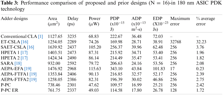
Furthermore, it is noted that ADP and EDP metrics of proposed adders are significantly better compared to other approximate adders considered for evaluation. Tab. 4 gives a brief comparison of power, delay, area, PDP and EDP metrics of proposed adders for various bit-widths in input operands (n = 8, 16, 32). It is noted from Tab. 4, area, power and PDP increase at the least by 1.8X, 1.8X and 3X proportion for 2X increase in input operand bit-width. Also, it is noted, the proportion of PDP rise of proposed adders is more for higher bit-widths in input operands.
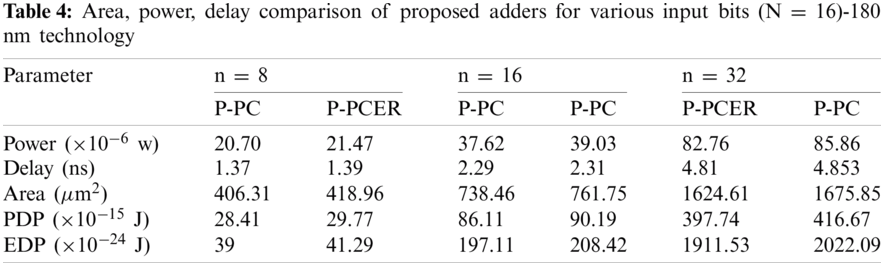
Fig. 6a shows the efficacy of proposed and other approximate adders in optimizing area and error through area vs. MRED plot, Figs. 6b and 6c exhibits the capability of proposed adders in optimizing ADP, PDP against error through NADP-MRED product and NPDP-MRED product plots. NADP and NPDP, defined as normalized ADP and PDP metrics, respectively, are calculated using (23) & (24).
where, ADPmax and PDPmax represent maximum ADP and PDP values of approximate systems compared.

Figure 6: Error-performance comparison of proposed and prior adders (a) Area vs. MRED, (b) NADP vs. MRED (c) NPDP vs. MRED
Note from Figs. 6b and 6c, P-PC and P-PCER adders demonstrate low NADP-MRED and NPDP-MRED products compared to ET-CSLA [16], SAET-CSLA [16], HPETA1 [17], HPETA2 [17], SARA [18], AEPA-FTFA1 [19] and AEPA-FTFA2 [19] adders. AEPA-EFA [19] design shows the least NADP-MRED and NPDP-MRED products compared to the proposed and other approximate adders. Conversely, the area of AEPA-EFA [19] is high, as noted from Fig. 6a. Also, from Fig. 6a, P-PC and P-PCER adders demonstrate the least area and MRED while ET-CSLA [16] demonstrate high MRED and moderate area. SAET-CSLA [16] exhibits high area and moderate MRED, HPETA1 [17] and HPETA2 [17] demonstrates high area and small MRED.
In addition, we have extracted power dissipation of P-PC and P-PCER adders against various operating frequency and temperature using transistor level schematics designed in Cadence Virtuoso design environment and simulations using Cadence Spectre. Fig. 7 shows the Power vs. frequency plot of P-PC adder in 90 and 180 nm ASIC PDK technology.
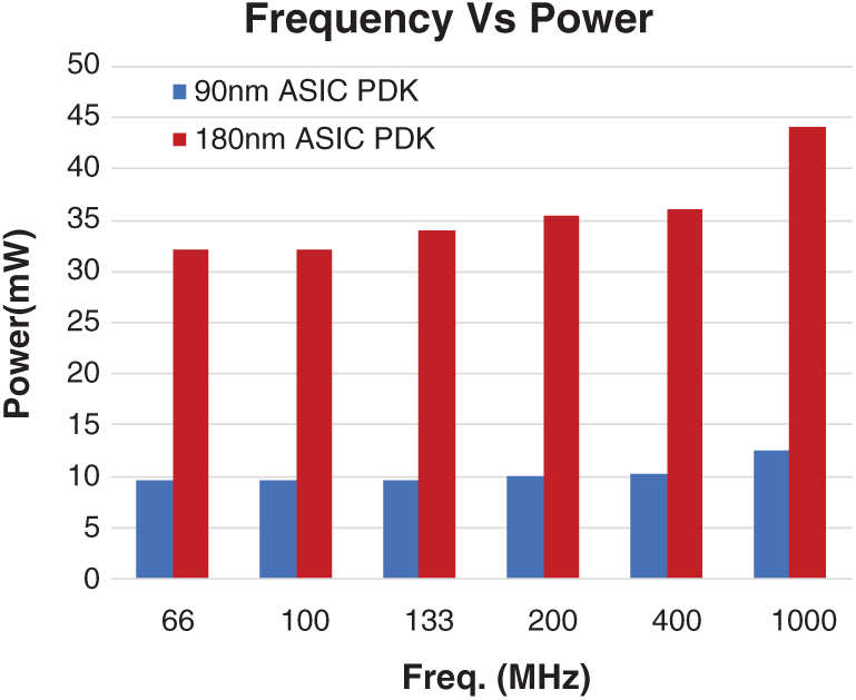
Figure 7: Power dissipation of P-PC adder against various operating frequency in 90 and 180 nm ASIC PDK technology
We have used supply voltage = 1 & 1.8 V for simulations with 90 and 180 nm ASIC PDK technology, respectively. Note from Fig. 7, the power dissipation increases linearly for a rise in frequency. Fig. 8 shows the power vs. temperature plots of proposed P-PC and P-PCER adders in 180 nm ASIC PDK. Note from Fig. 8, power dissipation of proposed adders decreases moderately for a rise in temperature in the range 27 to 120°C and exhibits functionality without any degradation.

Figure 8: Power dissipation of proposed designs against various operating temperature (Vdd = 1.8 V & f = 400 MHz)
5 Implementation in Digital Image Processing
To determine the novelty of the proposed approximate adders in fault-tolerant applications and verify their driving competence, implementations in image enhancement applications viz., filtering and blending are done in FPGA platform. The Verilog HDL models of the proposed adders and state-of-the-art approximate designs defined in literature are synthesized using Xilinx ISE 14.2, tool and hardware for the application system is prototyped on Spartan 6 FPGA (XC6XLX45-CSG324) device. Input images of size 256
To assess the performance of proposed P-PC and P-PCER adders in recurring addition, an implementation in Gaussian Filter (GF) is done. The Gaussian-smoothing filter is a 2-D convolution filter used to remove Gaussian noise and smoothen the noisy input image. Statistical noise having Probability Density Function (PDF) equal to that of the normal distribution is known as Gaussian noise. The PDF of Gaussian random variable is given by:
where, z = grey level, μ = mean value and σ = standard deviation.
Fig. 9 shows the block-level architecture of GF. 256

Figure 9: Block-level architecture of Gaussian filter
The quality metrics Mean Square Error (MSE) and Structural Similarity Index (SSIM) between output images processed by approximate and exact GF systems are used as a measure to evaluate the performance of the proposed approximate designs. MSE is given by (26).
where, a, b-size of the image; S (i, j) & S’ (i, j) are the exact and approximate filter outputs. Note that, from Fig. 10, SSIM and MSE values of output images processed by P-PC and P-PCER GFs are better compared to ET-CSLA [16], SAET-CSLA [16], HPETA1 [17], SARA [18], AEPA-FTFA1 [19] and AEPA-FTFA2 [19] GF systems. AEPA-EFA [19] GF system fare better SSIM and MSE compared to proposed and other approximate GFs. This is due to the exact FA cells used in the approximate logic of AEPA-EFA [19], limiting the maximum error to UBP-n/4.
On the other hand, ADP, PDP values of AEPA-EFA [19] are significantly high compared to all other approximate GFs. Note from Fig. 10, visual quality of processed images by P-PC, and P-PCER GFs are better and analogous with output image processed by standard GF. Output image processed by ET-CSLA [16] based GF exhibit poor visual quality with patches due to high error performance. In addition, we have extracted Average MSE (AMSE) metric using different output images processed by approximate GF systems with various standard input images-Lena, Boat, Cameraman, Bridge and Peppers and shown in Fig. 11. It is noted from Fig. 11, AMSE of P-PCER adder based GF is significantly reduced compared to P-PC and other approximate adder based GFs. AMSE of P-PC adder based GF is better compared to ET-CSLA [16], SAET-CSLA [16], HPETA1 [17], SARA [18], AEPA-FTFA1 [19] and AEPA-FTFA2 [19] based GFs.
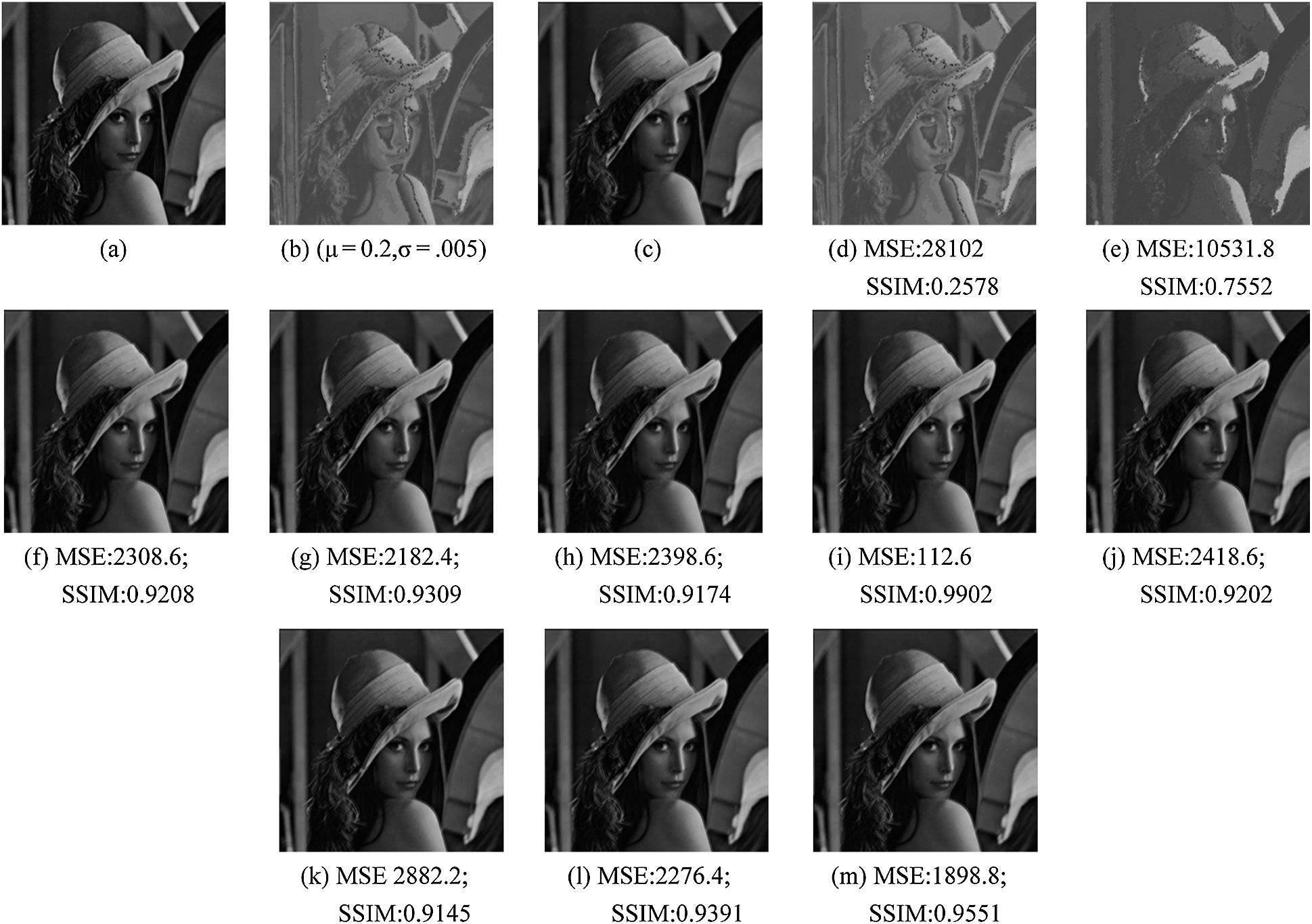
Figure 10: (a) Standard Image (b) 5% noisy image (c)–(n) Output images processed by Gaussian filter implemented using various adders (c) Conventional CLA [1] (d) ET-CSLA [16] (e) SAET-CSLA [16] (f) HPETA1 [17] (g) HPETA2 [17] (h) SARA [18] (i) AEFA-EFA [19] (j) AEFA-FTFA1 [19] (k) AEFA-FTFA2 [19] (l) P-PC adder (m) P-PCER adder
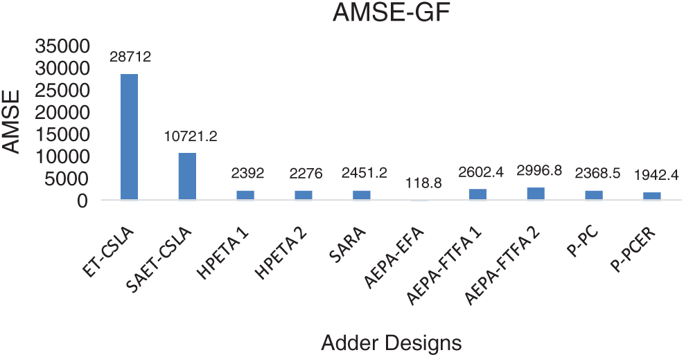
Figure 11: AMSE comparison of GF system implemented with proposed and prior approximate adders
Since GF system involves more than one adder, we have evaluated area, ADP and PDP metrics of the system with proposed and prior approximate adders in ASIC platform using Cadence Encounter with 180 nm PDK Technology and shown in Tab. 5. Note from Tab. 5, GF with P-PC and P-PCER adders fare 34.7% & 32.6%; 40.8% & 38.9%; 54.8% & 53.3%; 46.8% & 45.1%; 47.7% & 46.1%; 20.9% & 18.4%; 49.8% & 48.2%; 45.3% & 43.6% and 41% & 39.1% area reductions compared to conventional CLA [1], ET-CSLA [16], SAET-CSLA [16], HPETA1 [17], HPETA2 [17], SARA [18], AEPA-EFA [19], AEPA-FTFA1 [19] and AEPA-FTFA2 [19] based filter systems respectively.
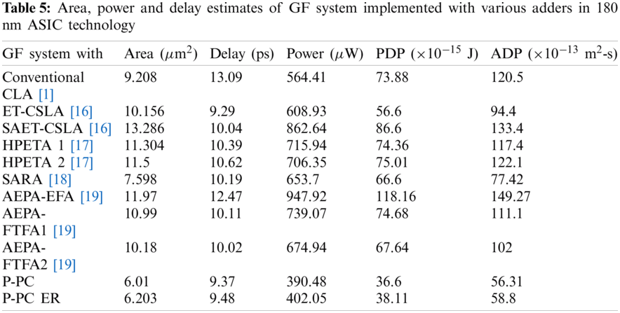
Consistently P-PC and P-PCER GFs demonstrate significant ADP reduction compared to all other approximate GF systems related. The processing speed of P-PC and P-PCER adder based GF systems are significantly improved compared to conventional CLA [1], SAET-CSLA [16], HPETA1 [17], HPETA2 [17], SARA [18], AEPA-EFA [19], AEPA-FTFA1 [19] and AEPA-FTFA2 [19] based system, thanks to the proposed parallel carry generation logic that reduces the critical delay of proposed adders. ET-CSLA [16] based GF system demonstrates the best processing speed compared to all other approximate systems. Conversely, the AMSE value of ET-CSLA [16] GF is enormous.
Image blending is the process of adding the corresponding pixel values of two input images of the same size. Pixel intensity values of the input images are scaled such that the pixel value of the resulting image does not exceed the maximum threshold. Fig. 12 shows the block-level architecture for image blending. Input images of size 256
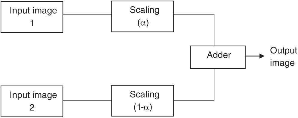
Figure 12: Block diagram of image blending system
Fig. 13 shows the output images processed by the image blending system implemented with proposed and prior approximate adders. Note from Fig. 13, SSIM and MSE values of output images processed by image blending system implemented with P-PC and P-PCER adders are significantly better compared to output images processed by adders considered for comparison. In addition, we have extracted the AMSE metric of various blending systems using processed images for various combinations of standard input images-Lena, Boat, Cameraman, Bridge and Peppers with α = 0.8, 0.5 & 0.2 and shown in Fig. 14. It is noted from Fig. 14, AMSE values of P-PC and P-PCER adder systems are significantly reduced compared to conventional CLA [1], ET CSLA [16], SAET-CSLA [16], HPETA1 [17], HPETA2 [17], SARA [18], AEPA-FTFA1 [19] and AEPA-FTFA2 [19] systems.

Figure 13: (a)–(b) Input images (c)–(n) Output images processed by Image blending system implemented using various adders. (c) Conventional CLA [1] (d) ET-CSLA [16] (e) SAET-CSLA [16] (f) HPETA1 [17] (g) HPETA2 [17] (h) SARA [18] (i) AEFA-EFA [20] (j) AEFA-FTFA1 [20] (k) AEFA-FTFA2 [20] (l) P-PC adder (m) P-PCER adder

Figure 14: AMSE comparison of Image blending system using various adders
In this article, we have proposed area-delay and energy optimized faithful approximate adders using parallel carry generation logic with reduced critical node capacitance. To trade-off error for trifling increase in area, error recovery units are used in the approximate part. Synthesis results with n-16 and 4-bit parallel carry generation block revealed that the proposed P-PC and P-PCER adders outperformed standard and other approximate designs in terms of area, ADP and PDP reductions. Functionality and driving capability of the proposed adders are evaluated with implementation in image de-noising and image blending systems. The superiority of proposed adders in image processing is demonstrated through a visual examination and structural similarity of processed outputs. At an instance, the proposed adders with n = 16 demonstrated at least 94% structural similarity and 42.4% & 43.7% decline in ADP and PDP, respectively, compared to the recent approximate design.
Acknowledgement: Thanks to the reviewing committee for their valuable points and notes.
Funding Statement: The author received no specific funding for this study.
Conflicts of Interest: The authors declare that they have no conflicts of interest to report regarding the present study.
1. D. Ercegovac and T. Lang, Digital Arithmetic, 1st ed., vol. 1. Amsterdam, Netherlands: Elsevier, pp. 51–129, 2004. [Google Scholar]
2. J. P. Uyemura, Introduction to VLSI Circuits and Systems. vol. 1. Hoboken, New Jersey: John Wiley & Sons, pp. 467–469, 2002. [Google Scholar]
3. J. P. Uyemura, CMOS Logic Circuit Design. vol. 10. Berlin, Germany: Springer Science & Business Media, pp. 392–404, 2007. [Google Scholar]
4. B. Ramkumar and H. M. Kittur, “Low-power and area-efficient carry select adder,” IEEE Trans. on Very Large Scale Integration (VLSI) Systems, vol. 20, no. 2, pp. 371–375, 2012. [Google Scholar]
5. J. Han, J. Honglan and L. Liu, Approximate Circuits Methodologies and CAD. Berlin, Germany: Springer, pp. 67–72, 2019. [Google Scholar]
6. M. Valinataj, “Fault-tolerant carry look-ahead adder architectures robust to multiple simultaneous errors,” Microelectronics Reliability, vol. 55, no. 12, Part B, pp. 2845– 2857, 2015. [Google Scholar]
7. M. A. Breuer and H. Zhu, “Error-tolerance and multi-media,” in Int. Conf. on Intelligent Information Hiding and Multimedia, Pasadena, CA, USA, pp. 521–524, 2006. [Google Scholar]
8. J. Han and M. Orshansky, “Approximate computing: An emerging paradigm for energy-efficient design,” in 18th IEEE European Test Symp., Avignon, France, pp. 1–6, 2013. [Google Scholar]
9. N. Zhu, W. L. Goh and W. Zhang, “Design of low-power high-speed truncation-error-tolerant adder and its application in digital signal processing,” IEEE Trans. Very Large Scale Integration Systems, vol. 18, no. 8, pp. 1225–1229, 2009. [Google Scholar]
10. O. Akbari, M. Kamal and M. Pedram, “RAP-CLA: A reconfigurable approximate carry look-ahead adder,” IEEE Transactions on Circuits and Systems—II: Express Briefs, vol. 65, no. 8, pp. 1089–1093, 2018. [Google Scholar]
11. V. Gupta, D. Mohapatra and A. Raghunathan, “Low-power digital signal processing using approximate adders,” IEEE Trans. on Computer-Aided Design of Integrated Circuits and Systems, vol. 32, no. 1, pp. 124–137, 2013. [Google Scholar]
12. P. Patali and S. T. Kassim, “High throughput FIR filter architectures using retiming and modified CSLA based adders, IET Circuits,” Devices & Systems, vol. 13, no. 7, pp. 1007–1017, 2019. [Google Scholar]
13. V. Gupta, D. Mohapatra and S. P. Park, “IMPACT: IMPrecise adders for low-power approximate computing,” in IEEE/ACM Int. Symp. on Low Power Electronics and Design, Fukuoka, Japan, pp. 409–414, 2011. [Google Scholar]
14. A. K. Verma, P. Brisk and P. Ienne, “Variable latency speculative addition: A new paradigm for arithmetic circuit design,” in 2008 Design, Automation and Test in Europe, Munich, Germany, pp. 1250–1255, 2008. [Google Scholar]
15. K. Al-Maaitah, G. Tarawneh and A. Soltan, “Approximate adder segmentation technique and significance-driven error correction,” in 27th Int. Symp. on Power and Timing Modeling, Optimization and Simulation, Thessaloniki, Greece, pp. 1–6, 2017. [Google Scholar]
16. R. Jothin and C. Vasanthanayaki, “High performance significance approximation error tolerance adder for image processing applications,” Journal of Electronic Testing, vol. 32, no. 3, pp. 377–383, 2016. [Google Scholar]
17. R. Jothin and C. Vasanthanayaki, “High performance error tolerant adders for image processing applications,” IETE Journal of Research, vol. 67, no. 2, pp. 205–216, 2018. [Google Scholar]
18. W. Xu, S. S. Sapatnekar and J. Hu, “A simple yet efficient accuracy-configurable adder design,” IEEE Trans. on Very Large Scale Integration Systems, vol. 26, no. 6, pp. 1112–1125, 2018. [Google Scholar]
19. P. Gnanambikai, K. N. Vijeyakumar and S. Kalaiselvi, “Area-efficient parallel adder with faithful approximation for image and signal processing applications,” IET Image Processing, vol. 13, no. 13, pp. 2587–2594, 2019. [Google Scholar]
20. J. Liang, J. Han and F. Lombardi, “New metrics for the reliability of approximate and probabilistic adders,” IEEE Trans. on Computers, vol. 62, no. 9, pp. 1760–1771, 2013. [Google Scholar]
 | This work is licensed under a Creative Commons Attribution 4.0 International License, which permits unrestricted use, distribution, and reproduction in any medium, provided the original work is properly cited. |