DOI:10.32604/cmc.2022.019527
| Computers, Materials & Continua DOI:10.32604/cmc.2022.019527 | |
| Article |
Defect Detection in Printed Circuit Boards with Pre-Trained Feature Extraction Methodology with Convolution Neural Networks
Electrical Engineering Department, College of Engineering, Shaqra University, Riyadh, 11911, Saudi Arabia
*Corresponding Author: Mohammed A. Alghassab. Email: Malghassab@su.edu.sa
Received: 15 April 2021; Accepted: 16 May 2021
Abstract: Printed Circuit Boards (PCBs) are very important for proper functioning of any electronic device. PCBs are installed in almost all the electronic device and their functionality is dependent on the perfection of PCBs. If PCBs do not function properly then the whole electric machine might fail. So, keeping this in mind researchers are working in this field to develop error free PCBs. Initially these PCBs were examined by the human beings manually, but the human error did not give good results as sometime defected PCBs were categorized as non-defective. So, researchers and experts transformed this manual traditional examination to automated systems. Further to this research image processing and computer vision came into actions where the computer vision experts applied image processing techniques to extract the defects. But, this also did not yield good results. So, to further explore this area Machine Learning and Artificial Intelligence Techniques were applied. In this study we have applied Deep Neural Networks to detect the defects in the PCBS. Pretrained VGG16 and Inception networks were applied to extract the relevant features. DeepPCB dataset was used in this study, it has 1500 pairs of both defected and non-defected images. Image pre-processing and data augmentation techniques were applied to increase the training set. Convolution neural networks were applied to classify the test data. The results were compared with state-of-the art technique and it proved that the proposed methodology outperformed it. Performance evaluation metrics were applied to evaluate the proposed methodology. Precision 94.11%, Recall 89.23%, F-Measure 91.91%, and Accuracy 92.67%.
Keywords: Printed circuit board; convolution neural network; inception; vgg16; data augmentation
Printed circuit boards (PCB) are included in almost all the electronic devices and it plays an important role in proper functioning of these devices. These components are being utilized in industrial usage for decades and for domestic purposes. There are many fields where PCBs are used such as logistics, defense, aeronautics and for the applications utilized for automobiles and industries related to medical, because PCBs are considered as the basic need for the design of electronic items. PCBs are made up of solid thin plates which are equipped with plastic coted materials like fiberglass, sometimes with composite epoxy which actually form a base to support the chips and electronic components [1,2].
These board are designed in such a way that would make pathways to form a circuit for the power electronic devices which are fixed to PCBs. PCBs need inspection for the proper functionality of the devices as the manufacturing is continuously increasing so also the inspection is getting on demand especially for the modern manufacturing. Industries like production and manufacturing are making utmost efforts in getting 100% quality assurance for the PCBs [3,4]. PCBs support various electronic components such as integrated circuits, transistors and capacitors as shown in Fig. 1. These components are mounted on the board by drilling holes and soldering them to form circuit pattern [5]. While undergoing these steps the PCBs could get spoiled and these are not in a position to be used in real and needs to be detected before exploring into the market. Inspection is very important step in the manufacturing and distribution of PCBs and needs to have 100% assured of all the parts. There are variety of approaches for automated inspections for PCBs during the past two decades. PCBs are in much demand as they are utilized in many consumer electronic gadgets such as laptops, tablets and smartphones. Based on this demand the manufacturing of PCBs is done in large quantities. So, the manufacturing of efficient and error free PCBs are essential and crucial. As they are manufactured in large quantities the accuracy and error free production is a big challenge and maintaining the quality is a big concern [6]. So, to overcome this challenge, inspection systems are deployed which could help in maintaining the quality of PCBs, but these teams are manual which are prone to error. So, automated inspection teams are needed which can prove to be efficient and less prone to errors. These automated inspection on PCBs also prove to be fast and detect the defects in the PCBs more accurately. Detecting the defected PCBs is very crucial because if it is not done with accuracy then it might lead to big destructions as the whole device might fail in proper functioning where these defected PCBs were installed. In the traditional methodology these defects in PCBs are detected by automatic inspection (AOI) machines [7]. After that a skilled quality inspection engineer would check all the PCBs. Many boards are classified as defected by AOI but, they are not. Since the machine has erroneously classified a PCB as defective based on some scratches or in the presence of tiny holes, dust particles like nanoparticles, paper fragments or even a small air bubble. Sometimes small difference about sample might also lead AOI machines to declare the PCB as defected as shown in Fig. 2. They are a need for efficient automated machines to handle these kinds of issues. Therefore, it is very essential to handle detection of defected PCBs more efficiently to prevent further obstacles and to fix the errors occurred by the visual inspection. Inspection of the PCBs consists of two major processes: Detection of defect and classification of defects. To overcome the errors and increase the defect detection accuracy image processing techniques are widely applied in PCBs manufacturing companies [8]. These image processing techniques can locate the parts in PCBs where the defects have occurred and further classify them. But, still they are some limitations in these techniques and to overcome those machine learning techniques are applied in the very recent times [7]. Detecting the defection in PCBs has been a source for many techniques being introduced. In the very recent times machine vision-based algorithm were presented, these techniques focused on automated detection of the defect. Machine vision-based techniques also helped in recognizing the different components in the PCB image. Depending on the situation and requirements, these techniques were implemented. These algorithms were categorized into certain number of classes and divided based on the requirement. Basically the algorithms are of four different types: Machine learning based [9,10], Projection types [11,12], algorithm based on filters [13,14], and finally hybrid methodologies [15,16]. In the current time machine learning is applied extensively, especially in solve image processing problems because of its ability to automatically produce discriminative features. These features are developed with little training samples with the help of introducing learning and pattern recognition algorithms. These algorithms include artificial neural network (ANN) and support vector machines (SVM). Currently with the development and introduction of deep learning which has attracted lot of researchers globally in various fields [17,18,19]. With the implementation of deep learning many real-time issues were handled efficiently, especially for long-standing machine-vision tasks that improved the classification accuracy significantly. These implementations include image segmentation [20] and also many image classification problems [21,22]. Because of the extra ordinary capability of deep learning it can be applied for PCBs defect detection. In PCB defect detection the uneven distribution of color which exists ion the chip location could be detected. This study is based on brightness improvement distribution on the PCB images. As discussed above manual detection is done by trained engineers which are failing at sometimes because of the limitations, to overcome this issue an automated system should be introduces which can do this job more efficiently. So, machine learning based techniques which is both accurate and fast in detecting the defects in PCB images are introduced with the help of deep learning techniques. The objective of this research is to introduce deep learning techniques to detect the defection in the PCB images which can reduce the false detection rate and further increase the production rate. According to few studies like this [23], it has revealed that deep learning is outperforming traditional machine learning approach for classification and algorithms used for extraction of features. In another work which is related to PCBs defect detection also have applied deep learning approach [24-26]. Other approaches are also implemented for PCBs like [27] which is based on template-matching. Similarly, another approach for PCB defect detection is applied [28], in this method the authors have used OpenCV for image subtraction. There are so many methodologies applied but convolution neural network (CNN) is applied in many applications like [29,30], where the core idea is image recognition for the detection of objects.
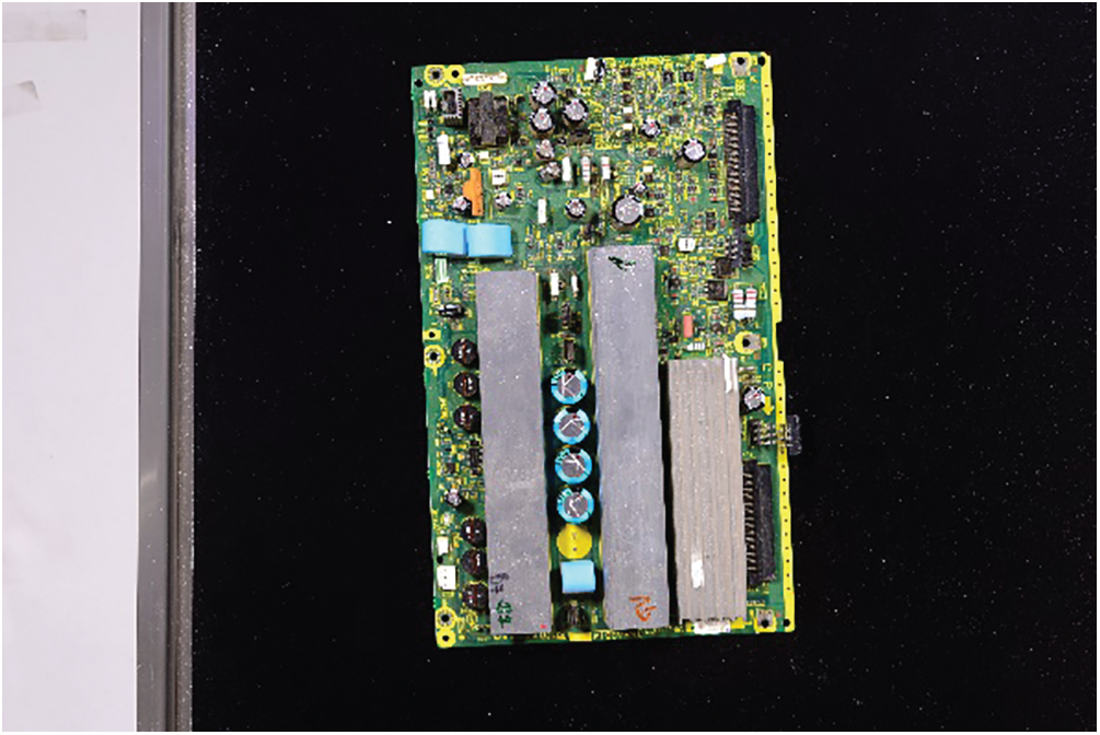
Figure 1: Basic printed circuit board with all the components
The rest of the paper is as follows: Section 1 give the full introduction about the research field, Section 2 discusses the literature review, Section 3 describes the dataset used in this study and also image pre-processing and data augmentation details, Section 4 discussed the actual proposed methodology, followed by Section 5 discuss the implementation, and Section 6 with results and analysis and Section 7 has the conclusion and Section 8 with discussion followed by references.
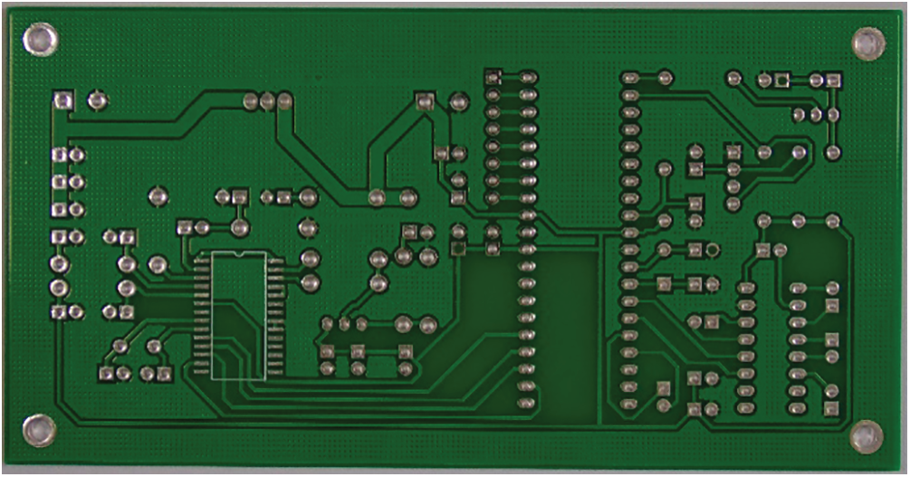
Figure 2: Printed broad circuit without the extra components to detect the defect on the board
Detecting the defects in PCB could be classified into two types: image processing-based techniques, machine learning based techniques, and object detection method. In the image processing technique, the errors are detected on the PCB images and then classify them if found any error. Some of the techniques are listed as shown in the Tab. 1.
Image processing-based techniques: Further to this research, the authors of this work [31], have introduced a PCB inspection system to detect the defect in PCB bars by applying image processing techniques. The outcome of this method is recognition of common defects such as missing of holes and open circuits. In another work [6] the authors have introduced an automated visual inception system for detecting the defects in PCBs. A template image is used as reference and then mapped with the real PCB image and if any difference is found after subtraction then the inspected image is classified as defected. The authors in this work [5], have collected all the possible defects that could occur on PCBs and introduce a MATLAB based image processing technique to classify them. They have discovered 14 different types of defects which were further classified into 5 different groups. In another approach, the authors in this work [32] have introduced a unique methodology based on morphological image segmentation for detecting the defects in PCBs and classify them as defected, the approach is image segmentation algorithm together with image processing theories. Another image processing technique is applied to detect the defect in PCBs. In this work [33], the authors have applied wavelet-based image difference algorithm. This is an automatic system which checks the difference in wavelet form and classifies the image as defected if it finds some difference with the template image. A different approach is adapted in this work [34], the authors have tried hybrid methodology by combining genetic algorithm and neural network classifier to detect the defect in PCB.
Machine learning based techniques: Feature extraction was done by genetic algorithms. PCBs had another type of defect caused by solder-balls, this defect was studied by [35], they detected this defect with the help of data mining approach. The authors in this work [36] have adapted latest machine learning technique called deep learning as it best suited for dataset without unstructured and unlabelled data. In this work they have compared the result with different machine learning classifiers like support vector machine to detect the defects in PCBs. In another work [8] Convolution neural networks (CNN) was applied as a classification algorithm to detect defects in PCBs. Similarly in another approach [37] CNN is applied to recognize the defects in PCBs. Deep discriminative features were applied to detect the defect in PCBs [38]. The defects were located by applying sliding window approach. In another approach, the authors in [39] applied Auto-VRS technique. It uses deep neural networks to check if the defects detected with correct or not. A multi-label learning problem was handled by [40], in this work multi-task convolution neural network was proposed. The proposed methodology developed a model which has the capability of defining label learning like a binary classification task. Deep learning technique was applied to detect the defects in PCBs by [41], in this work DeepPCB dataset was used which has 1500 images. These images are pairs of defective and intact PCBs. In another work [42] related deep learning. The authors have proposed a new approach by utilizing Autoencoder for the extraction of discriminative features.
Object detection method: Object detection methodology can be efficiently applied in PCBs to detect any defects. Based on this assumption many researchers have proposed this technique, some of them are discussed here. In recent time numerous generic object detection techniques are proposed as discussed in [43]. Some of the as example are two stage methodology (e.g., RCNN [44], and FastRCNN [45]) and some are based on single stage detection like (e.g., YOLO [46] and SSD [47]), all these techniques have demonstrated excellent accuracy by applied the dataset presented in [43]. Recently object recognition technique is extensively applied for PCBs defect detection. Some of the works are discussed here. In this work [48], the authors have proposed machine learning and Deep learning both for the detection of PCB components by applying AdaBoost classifier to detect the capacitors ion the PCBs. Similarly in [49,50], they have applied DL to investigate the PCB components. In [49], they have made an intensive analysis by applying YOLO architecture to find the capacitors and resistors on the PCBs. In [50], object detection technique is applied which was based on neural networks to identify numerous PCB components like capacitors, resistors, and other smaller components. Some of the major electronic components where PCBs could be implemented are [51] and [52].

The dataset used in this work for the training of proposed methodology and development of the model is DeepPCB. This dataset is used for the detection of defects in PCBs. It consists of 1500 pairs of images, where one image in the pair is a template image and the other is the defected image. There are six types of defects annotated to the test images. The defected images are names as open, short, mousebite, spur, pin hole and spurious copper. This dataset is freely available to the research community. The following are the advantages of this dataset: a) The images of each corresponding pairs (template and test image with defects) are aligned by template matching methodology. This technique of aligning the images already reduces lots of efforts especially for the image pre-processing. b) This dataset is available for free as shown in Fig. 3. It can be used by the researchers to detect the defect in PCB as the dataset is available publicly. This dataset is collected by following the regulations of common industrial settings. The images collected are obtained with the help of linear scan CCD with the resolution of around 48 pixels per 1 millimetre. The clean image which defect-free acting as template image is collected manually and further it is monitored and dressed in respect to the sample image. The raw size of the image for both template and defected are 16k × 16k pixels. These raw size images are then clipped and reshaped to sub-images with new size as 640 × 640 pixles and then they are aligned with template matching method. This methodology reduces the translation and rotation offset among the pairs of the images. Further to the data collection process, a threshold is then carefully designed to apply binarization for avoiding the disturbances caused by illumination. Image pre-processing is also applied depending on the PCB defects. The techniques are image registration and thresholding, these techniques are applied to get high-accuracy PCB defect localization [26]. The images are annotated by applying axis-aligned bounding box technique. The images were annotated into six types and each one with a defect type. The following were the annotation name of PCB defects: open, short, mouse bite, spur, pin hole and spurious copper.
The PCB images were applied for image processing. There are various image pre-processing techniques available like smoothing, background subtraction, resizing etc. These techniques are applied to enhance the quality of the image and make it able for any kind of Machine Learning technology.
Data augmentation technique is applied on the images of the dataset if the size of the dataset is not enough to be implemented on deep learning neural network. Since deep learning technique needs lot of data to process and train the model. To be able to train and test the proposed model in deep learning, the size of the dataset should be increased. To increase the size few techniques are needed to be applied such as cropping, rotating, scaling, translating and flipping. There are few other techniques like Generative Adversarial Networks (GANs) which are applied to generate new images for training which have proved in the past to be more significant especially for data generation task. The purpose of applying data augmentation is not only increasing the data size but also this approach improves the current state of the art classification task. In another study feature-space and data-space can also be used to perform data augmentation.
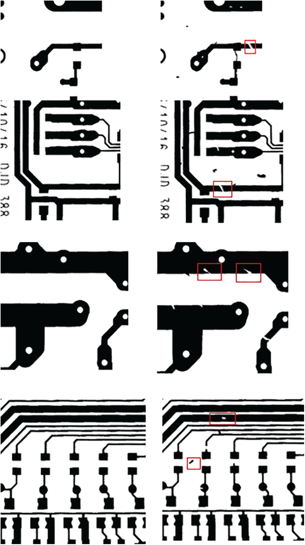
Figure 3: DeepPCB sample pair images of both template and defected image
The proposed model in this work takes care of only one class for training and the goal is to extract features which are not similar concerning the normal samples. The following is the architecture designed for neural network. The desired outcomes would be: a) the proposed model should extract the comprehensive features for the normal samples. The purpose is to distinguish between normal and defective samples based on the features, b) this designed architecture should be flexible and can be adopted to other domains.
Convolution Neural Network (CNN) in the current times has proved to be an efficient technique for image classification and detection of objects, as shown in Fig. 4. But, the training process of CNN needs a big amount of data to train the proposed model and it needs extensive computation power. Keeping this in mind the researchers have proposed an alternative to overcome this shortcoming by introducing transfer learning technique. This technique is proved to be efficient especially for the experimentation where the training data is in limited size [53]. The basic idea behind transfer learning is based on the learning done on one specific problem could be re-used for solving different set of problems. The layers in CNN which is trained be: Starting layers are learned to produce generic low-level image representations like blobs and textures. The later layers are responsible for producing high level of semantic representations for the output. ImageNet [54] dataset is used for training the model which is not similar to PCBs dataset, but he advantage of using ImageNet is its number of images trained which proves to be robust for the next level of learning the different datasets for the extraction of features.
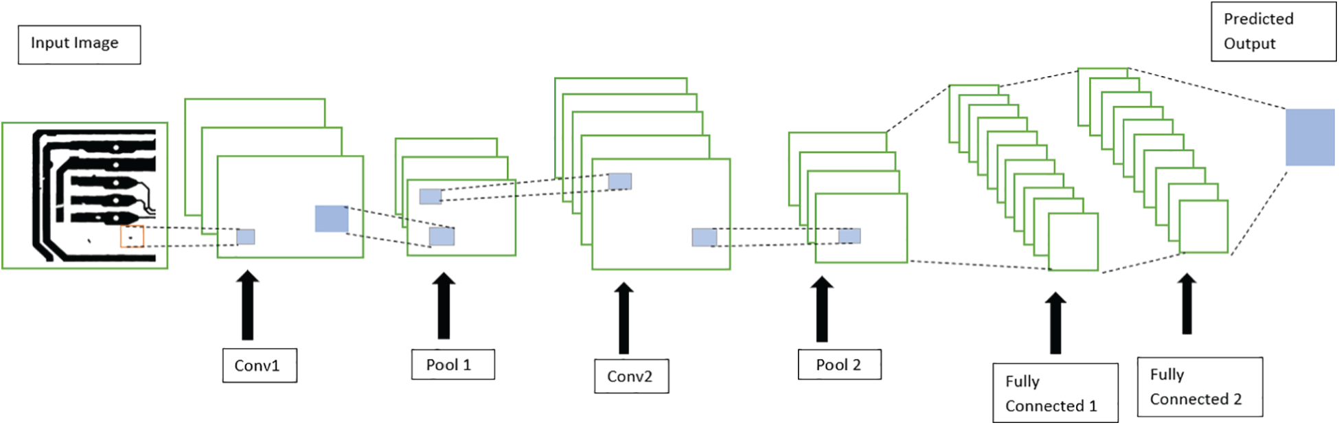
Figure 4: Basic building block of convolution neural networks
The problem in this study is portraited as detection of anomaly wherein the defects are calculated without much collection of big data related to defects, but rather discover the important features which would help in detecting the defects in the image. In this work transfer learning approach is implemented which is considered as the common approach to extract features and further gives a customized data. Here the transfer learning is done based on VGG16 network [55]. It is a deep neural network which has 16 layers (13 of them are convolution and the rest are fully connected as shown in Fig. 5. This network was trained to classify images with 1000 categories. The total images used for training are around 1 million. ImageNet dataset is used to train this network with the available pertained weights for transfer learning. Features are extracted based on different approaches for custom image datasets. These approaches cold be removing the final fully connected layer or sometimes beginning layers are frozen with retraining the other layers based on the custom dataset. As a regular practice it is used for supervised transfer learning, the last layer has neurons equal to the number of classes corresponding to the training model for classification. The original features vector for fc2 is 4096 dimensions and further the final output of the convolution is around 25,099 elements.
The proposed approach has two main parts: Initially we apply VGG16 pretrained convolution layers which are frozen to extract the features. Then, in the second phase we follow the approach presented in [56], this technique is based on unsupervised representation of learning on simple geometric transformations. By following this step, it is expected to give a rich data representation for transfer learning. This data is then fine-tuned for representing as training data. After transfer learning approach, several experiments were conducted for the optimum VGG16. As shown in the figure is the most efficient VGG16 configuration which proved to be successful. The description of our configured VGG16 is as follows: all the layers of VGG16 were frozen starting from the input layer till the flatten layer, after freezing these layers then we detached the final layers fc1 and fc2 layers and upon that new two dense layers were added. These two layers had 1000 and 66 neurons respectively. After all these changes softmax layer was added. The parameters which were output from the frozen layers are served as an input to the FC1.
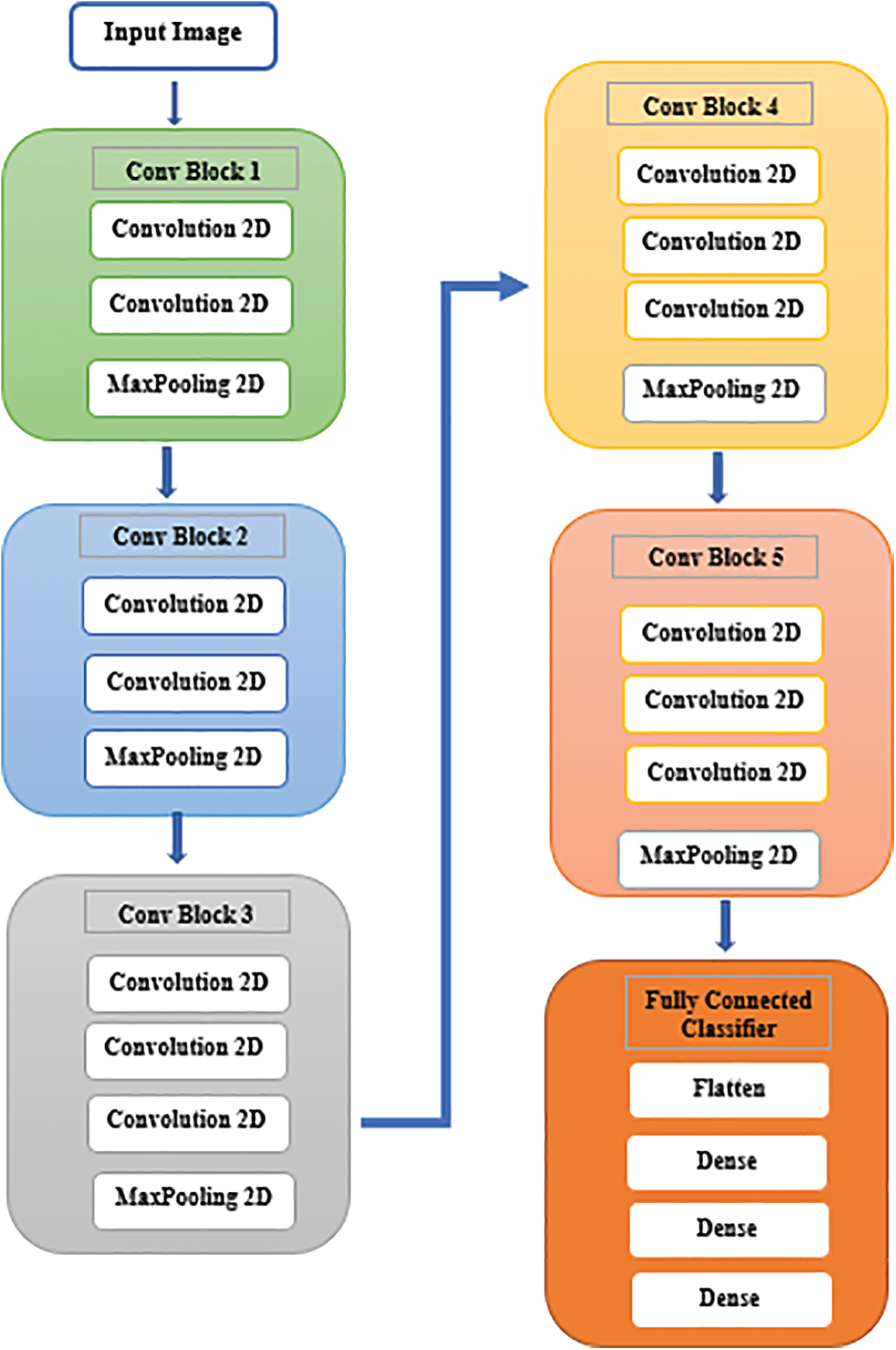
Figure 5: A building block of VGG16 pretrained network
Another pretrained model is utilized to extract the features for classification. In this process Inception-V3 network [57] is applied. This network is also trained on ImageNet dataset for the purpose of feasibility study in the mid-level for the extraction of features for further classification of PCB images. The mid-level representations [58] of the PCB images are extracted from the output of the third Inception module i.e., ‘Mixed-2’ layer of the Inception-V3 network as shown in Fig. 6. Inception module consists of multiple-sized convolutional filters which provide features at different scales. We train an adaptation network, consisting of three convolutional layers, one max pool layer and two fully connected layers, using the extracted mid-level representations of the PCB images. The combination of the pre-trained Inception-V3 network up to its ‘Mixed-2’ layer and the adaptation network trained on the midlevel representations provides the complete CNN to classify the PCB images.
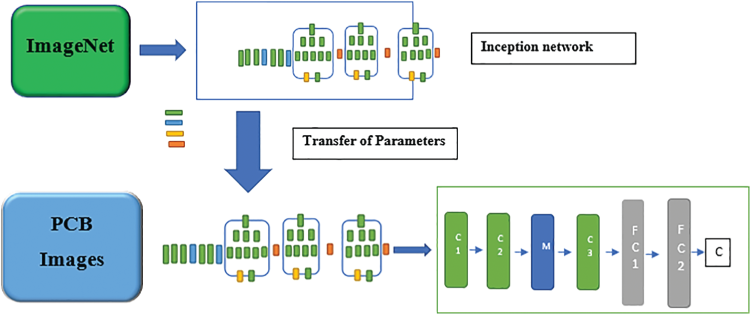
Figure 6: Inception pretrained network architecture
As can be seen in the below Fig. 7 which gives the clear picture about the implementation steps being carried on in this research. Initially DeepPCB dataset is downloaded which consists of 1500 paired images of both defected and non-defected images as discussed in the dataset section of this paper. Then pre-processing steps were applied wherein image processing techniques were applied on the PCB images. Then pretrained networks are applied to extract relevant features and after that image classification technique is implemented to detect the defects in the images.
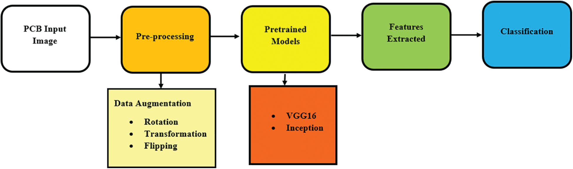
Figure 7: Overall workflow of proposed method
The process of defect detection includes threshold methodology. The difference between the template image and the defected image is calculated based on the threshold. The amount of difference would determine the possibility of the image being defected. The defect is calculated if the difference in the two images crosses the threshold, then the image is considered as a defective image. If the difference is below the threshold then is considered as non-defective image. In this proposed method this threshold is determined which categorizes the image. The best threshold is calculated based on true positive rate recall, precision, selectivity, accuracy and, F-score. The evaluation of the proposed methodology could be evaluated based on these four equations. These equations would estimate the accuracy of prediction for the input images if they belong to defected image or non-defected image. The following are the parameters in these equations: True Positive (TP), False Positive (FP), True Negative (TN), and False Negative (FN). Here TP represents the correctly classified positive cases, TN represents the correctly classified negative cases, FP represents as the positive cases being classified incorrectly, FN represents the negative cases being incorrectly classified. After all these parameters, the exact measurement is further evaluated based on the accuracy which ultimately interprets the performance of the proposed model. The accuracy is expressed by using TP, TN, FP, FN as represented by Eq. (1). The other significant performance metric for multi-class classification are precision recall, and F1-score are expressed using Eqs. (2)–(4) respectively. The results of evaluation metrics are as shown in the Tab. 2.
As it is shown in Tab. 2 when threshold equal to 100 the accuracy is maximum, and it is equal to 0.986. It should be noted that this threshold works fine with all kinds of defects. The proposed methodology was implemented using Python, TensorFlow and Keras framework. We have taken 100 images in random and the accuracy of detecting the defects were very good. Testing was done on 80 PCB images. The following are the defect detection categories discovered in this study. “Missing hole” is a kind of defect which was detected lowest because all the incorrect holes were incorrectly identified and located. There is another reason for the detection of low defects, like threshold estimation. If the results are measured by evaluation metrics, then sensitivity was around 94% and specificity of 92%. Another reason for better results is the technical system which has pre-trained models for the extraction of discriminative features for detecting the defects. The Unsupervised learning had good information which used to extract useful knowledge from the unlabeled data. Transfer Learning also proved handy for the excellent results which helped in extracting the relevant information. This approach also helped in escaping the overfitting issue, this overfitting occurs when the machine cannot adequately understand the structure of the data since the results in the model does not fit because it is insufficient and also because if the smaller number of relevant features. Apart from Transfer learning, data augmentation also played an important role which forced the model to extract the relevant features which were considered as useful and essential for the detection of defects. The information extracted by rotating the images helped in enhancing the defect detection accuracy. This approach helps in getting more training data which would make the model more robust and efficient to tackle other serious issues. The results as shown in Tab. 3. describes the test set classification accuracy achieved based on the proposed pretraining models. The comparison is done with the results of other methodologies [24] and the proposed methodology of detecting the defects in PCBs. As can be seen in the Tab. 3, the proposed methodology is giving good results for classifying the defected PCBs. The accuracy achieved by [24] is 70.8% and the proposed technique achieved better results. Now it is confirmed that the proposed methodology with Transfer Learning outperformed the high-level representation method [24]. The comparison is done between features extracted traditionally which was based on engineering and further classifying them to detect the defects more often based on predefined PCB conductor shape and illumination patterns. Then the comparison is done with the Transfer Learning based approach which helps is improving and increasing the training data which reflects in enhancing the classification accuracy.


Printed Circuit Board are used in almost every electronic device. The functionality of these devices strongly depends on the PCBs being implemented in them. If the PCB is defected, then no matter how good the devices is designed it would give a disastrous performance. So, proper implementation and proper development of PCBs are the most important thing. Initially these PCBs were checked manually by human beings with their naked eyes which had many issues as defected PCBs were considered as good and the prefect PCBs were categorized as defected because of the human error. When this thing happened very commonly the researchers took this issue and tried to solve it automatically by developing automated systems. These automated systems were developed based on the latest technologies. Computer vision and image processing came into picture with its ability to detect the objects. There are many image processing techniques available to detect the object. In this work DeepPCB dataset was used to detect the defects in the PCB images. Convolution neural networks were applied. Feature extraction techniques were applied especially pretrained VGG16 and Inception networks were applied to extract the relevant features. Transfer Learning were applied to the training dataset. Before that data pre-processing and data augmentation techniques were applied to increase the training data to make the model more robust. Ultimately by applying pretrained models the accuracy was measured with performance metrics and finally compared our proposed method with some other methods. These comparative analyses clearly stated that the proposed method outperformed other methods in detecting the defects in the PCBs.
In this work Printed Circuit Board images are studied for any defects in them. DeepPCB dataset is used for this study. The dataset has pairs for defect and non-defect images. The non-defected images are considered as template images. Data pre-processing steps are applied to the images with data augmentation techniques like rotation, flipping and transformation. This data augmentation helped in increasing the training data size which helps in making a goof training model. Transfer learning technique is applied using ImageNet dataset to increase the feature counts. After pre-processing and data augmentation, a pretrained models were applied to extract most relevant features. VGG16 and Inception networks were applied to the training data to extract most relevant and discriminative features. These pretrained models helped in classifying the defected PCBs from that of the non-defective's PCB images. Finally, we have compared our results with others work who used only traditional feature extraction techniques. The results show that the proposed methodology outperformed other methods.
9 Limitations and Future Scope
In this work the defects in the PCB were detected. But more accuracy could be achieved by applying more recent feature extraction and pretrained models. Also, this technique could be applied on other applications like detecting the defects in plastic injection molding products.
Funding Statement: The author would like to thank Deanship of Scientific Research at Shaqra University for their support to carry this work.
Conflicts of Interest: The author declare that they have no conflicts of interest to report regarding the present study.
1. H. S. Cho, J. G. Yoo, J. S. Kim and S. H. Kim, “Samsung electro mechanics Co Ltd. official gazette of the United States patent and trademark. printed circuit board,” US Pat. US, vol. 8, no. 159, pp. 824, 2012. [Google Scholar]
2. H. Matsubara, M. Itai and K. Kimura, “NGK spark plug Co Ltd. patents assigned to NGK spark plug. printed circuit board,” U.S. Patent US6,573,458, issued September 12, 2003. [Google Scholar]
3. A. P. S. Chauhan and S. C. Bhardwaj, “Detection of bare PCB defects by image subtraction method using machine vision,” in The World Congress on Engineering(WCE 2011London, U.K., pp. 6–8, 2011. [Google Scholar]
4. N. K. Khalid “An image processing approach towards classification of defects on printed circuit board,” Ph.D. dissertation, Universiti Teknologi Malaysia, Malaysia, 2007. [Google Scholar]
5. K. Kamalpreet and K. Beant, “PCB defect detection and classification using image processing,” International Journal of Emerging Research in Management & Technology, vol. 3, no. 8, pp. 1–10, 2014. [Google Scholar]
6. W. Y. Wu, M. J. J. Wang and C. M. Liu, “Automated inspection of printed circuit boards through machine vision,” Computers in Industry, vol. 28, no. 2, pp. 103–111, 1996. [Google Scholar]
7. P. Wei, C. Liu, M. Liu, Y. Gao and H. Liu, “CNN-Based reference comparison method for classifying bare PCB defects,” Journal of Engineering, vol. 2018, no. 16, pp. 1528–1533, 2018. [Google Scholar]
8. K. P. Anoop, N. S. Sarath and V. V. Kumar, “A review of PCB defect detection using image processing,” International Journal of Engineering and Innovative Technology, vol. 4, no. 11, pp. 188–192, 2015. [Google Scholar]
9. F. L. Chen and S. F. Liu, “A neural-network approach to recognize defect spatial pattern in semiconductor fabrication,” IEEE Transactions on Semiconductor Manufacturing, vol. 13, no. 3, pp. 366–373, 2000. [Google Scholar]
10. C. T. Su, T. Yang and C. M. Ke, “A neural-network approach for semiconductor wafer post-sawing inspection,” IEEE Transactions on Semiconductor Manufacturing, vol. 15, no. 2, pp. 260–266, 2002. [Google Scholar]
11. D. B. Perng and S. H. Chen, “Directional textures auto-inspection using discrete cosine transform,” International Journal of Production Research, vol. 49, no. 23, pp. 7171–7187, 2011. [Google Scholar]
12. D. M. Tsai and S. C. Lai, “Defect detection in periodically patterned surfaces using independent component analysis,” Pattern Recognition, vol. 41, no. 9, pp. 2812–2832, 2008. [Google Scholar]
13. W. C. Li and D. M. Tsai, “Wavelet-based defect detection in solar wafer images with inhomogeneous texture,” Pattern Recognition, vol. 45, no. 2, pp. 742–756, 2012. [Google Scholar]
14. D. M. Tsai and B. Hsiao, “Automatic surface inspection using wavelet reconstruction,” Pattern Recognition, vol. 34, no. 6, pp. 1285–1305, 2001. [Google Scholar]
15. C. H. Wang, “Separation of composite defect patterns on wafer bin map using support vector clustering,” Expert Systems with Applications, vol. 36, no. 2, pp. 2554–2561, 2009. [Google Scholar]
16. T. S. Li, “Applying wavelets transform, rough set theory and support vector machine for copper clad laminate defects classification,” Expert Systems with Applications, vol. 36, no. 3, pp. 5822–5829, 2009. [Google Scholar]
17. Y. LeCun, Y. Bengio and G. Hinton, “Deep learning,” Nature, vol. 521, no. 7553, pp. 436–444, 2015. [Google Scholar]
18. A. S. Chivukula and W. Liu, “Adversarial deep learning models with multiple adversaries,” IEEE Transactions on Knowledge and Data Engineering, vol. 31, no. 6, pp. 1066–1079, 2018. [Google Scholar]
19. L. Li, N. Sang, L. Yan and C. Gao, “Motion-blur kernel size estimation via learning a convolutional neural network,” Pattern Recognition Letters, vol. 119, no. 1, pp. 86–93, 2019. [Google Scholar]
20. L. C. Chen, G. Papandreou, I. Kokkinos, K. Murphy and A. L. Yuille, “Deeplab: Semantic image segmentation with deep convolutional nets, atrous convolution, and fully connected crfs,” IEEE Transactions on Pattern Analysis and Machine Intelligence, vol. 40, no. 4, pp. 834–848, 2017. [Google Scholar]
21. D. Ciregan, U. Meier and J. Schmidhuber, “Multi-column deep neural networks for image classification,” in IEEE Conf. on Computer Vision and Pattern Recognition(CVPR 2012Providence, Rhode Island, pp. 3642–3649, 2012. [Google Scholar]
22. T. H. Chan, K. Jia, S. Gao, J. Lu, Z. Zeng et al., “PCANet: A simple deep learning baseline for image classification?,” IEEE Transactions on Image Processing, vol. 24, no. 12, pp. 5017–5032, 2015. [Google Scholar]
23. Y. Bengio, A. Courville, and P. Vincent, “Representation learning: A review and new perspectives,” IEEE Transactions on Pattern Analysis and Machine Intelligence, vol. 35, no. 8, pp. 1798–1828, 2013. [Google Scholar]
24. Y. Takada, T. Shiina, H. Usami, Y. Iwahori and M. K. Bhuyan, “Defect detection and classification of electronic circuit boards using keypoint extraction and CNN features,” in The Ninth Int. Conf. on Pervasive Patterns and Applications Defect (PATTERNS 2017Athens, Greece, pp. 113–116, 2017. [Google Scholar]
25. P. S. Malge and R. S. Nadaf, “PCB defect detection, classification and localization using mathematical morphology and image processing tools,” International Journal of Computer Applications, vol. 87, no. 9, pp. 1–14, 2014. [Google Scholar]
26. D. B. Anitha and M. Rao, “A survey on defect detection in bare PCB and assembled PCB using image processing techniques,” in Int. Conf. on Wireless Communications, Signal Processing and Networking (WiSPNET 2017Chennai, India, pp. 39–43, 2017. [Google Scholar]
27. A. J. Crispin and V. Rankov, “Automated inspection of PCB components using a genetic algorithm template-matching approach,” International Journal of Advanced Manufacturing Technology, vol. 35, no. 3, pp. 293–300, 2007. [Google Scholar]
28. W. Ce, “PCB defect detection USING OPENCV with image subtraction method,” in Int. Conf. on Information Management and Technology (ICIMTech 2017Yogyakarta, Indonesia, pp. 204–209, 2017. [Google Scholar]
29. H. Hosseini, B. Xiao, M. Jaiswal and R. Poovendran, “On the limitation of convolutional neural networks in recognizing negative images,” in 16th IEEE Int. Conf. on Machine Learning and Applications (ICMLA 2017Cancun, Mexico, pp. 352–358, 2017. [Google Scholar]
30. X. Tao, Z. Wang, Z. Zhang, D. Zhang, D. Xu et al., “Wire defect recognition of spring-wire socket using multitask convolutional neural networks,” IEEE Transactions on Components, Packaging and Manufacturing Technology, vol. 8, no. 4, pp. 689–698, 2018. [Google Scholar]
31. N. Dave, V. Tambade, B. Pandhare and S. Saurav, “PCB defect detection using image processing and embedded system,” International Research Journal of Engineering and Technology, vol. 3, no. 5, pp. 1897–1901, 2016. [Google Scholar]
32. S. H. I. Putera and Z. Ibrahim, “Printed circuit board defect detection using mathematical morphology and MATLAB image processing tools,” in 2nd Int. Conf. on Education Technology and Computers (ICETC 2010Shanghai, China, pp. 359–363, 2010. [Google Scholar]
33. Z. Ibrahim, S. A. R. Al-Attas, Z. Aspar and M. M. Mokji, “Performance evaluation of wavelet-based PCB defect detection and localization algorithm,” in IEEE Int. Conf. on Industrial Technology, (IEEE ICIT’02Bankok, Thailand, pp. 226–231, 2002. [Google Scholar]
34. P. K. Srimani and V. Prathiba, “Adaptive data mining approach for PCB defect detection and classification,” Indian Journal of Science and Technology, vol. 9, no. 44, pp. 1–9, 2016. [Google Scholar]
35. A. Kusiak and C. Kurasek, “Data mining of printed-circuit board defects,” IEEE Transactions on Robotics and Automation, vol. 17, no. 2, pp. 191–196, 2001. [Google Scholar]
36. T. Vafeiadis, N. Dimitriou, D. Ioannidis, T. Wotherspoon, G. Tinker et al., “A framework for inspection of dies attachment on PCB utilizing machine learning techniques,” Journal of Management Analytics, vol. 5, no. 2, pp. 81–94, 2018. [Google Scholar]
37. V. A. Adibhatla, J. S. Shieh, M. F. Abbod, H. C. Chih, C. C. Hsu et al., “Detecting defects in PCB using deep learning via convolution neural networks,” in 13th Int. Microsystems, Packaging, Assembly and Circuits Technology Conf. (IMPACT 2018Taipei, Taiwan, pp. 202–205, 2018. [Google Scholar]
38. C. Zhang, W. Shi, X. Li, H. Zhang and H. Liu, “Improved bare PCB defect detection approach based on deep feature learning,” Journal of Engineering, vol. 2018, no. 16, pp. 1415–1420, 2018. [Google Scholar]
39. Y. S. Deng, A. C. Luo and M. J. Dai, “Building an automatic defect verification system using deep neural network for pcb defect classification,” in 4th Int. Conf. on Frontiers of Signal Processing (ICFSP 2018Poitiers, France, pp. 145–149, 2018. [Google Scholar]
40. L. Zhang, Y. Jin, X. Yang, X. Li, X. Duan et al., “Convolutional neural network-based multi-label classification of PCB defects,” Journal of Engineering, vol. 2018, no. 16, pp. 1612–1616, 2018. [Google Scholar]
41. S. Tang, F. He, X. Huang and J. Yang, “Online pcb defect detector on a new pcb defect dataset,” in IEEE Conf. on Computer Vision and Pattern Recognition (CVPR 2019Long Beach, CA, pp. 1–5, 2019. [Google Scholar]
42. A. Mujeeb, W. Dai, M. Erdt and A. Sourin, “One class based feature learning approach for defect detection using deep autoencoders,” Advanced Engineering Informatics, vol. 42, no. 1, pp. 100933, 2019. [Google Scholar]
43. L. Jiao, F. Zhang, F. Liu, S. Yang, L. Li et al., “A survey of deep learning-based object detection,” IEEE Access, vol. 7, pp. 128837–128868, 2019. [Google Scholar]
44. R. Girshick, J. Donahue, T. Darrell and J. Malik, “Rich feature hierarchies for accurate object detection and semantic segmentation,” in IEEE Conf. on Computer Vision and Pattern Recognition (CVPR14Columbus, Ohio, pp. 580–587, 2014. [Google Scholar]
45. R. Girshick, “Fast r-cnn,” in IEEE Int. Conf. on Computer Vision (ICCV 2015Santiago, Chile, pp. 1440–1448, 2015. [Google Scholar]
46. J. Redmon, S. Divvala, R. Girshick and A. Farhadi, “You only look once: Unified, real-time object detection,” in IEEE Conf. on Computer Vision and Pattern Recognition (CVPR 2016Las Vegas, NV, USA, pp. 779–788, 2016. [Google Scholar]
47. W. Liu, D. Anguelov, D. Erhan, C. Szegedy, S. Reed et al., “Ssd: Single shot multibox detector,” in European Conf. on Computer Vision (ECCV2016Amsterdam, The Netherlands, pp. 21–37, 2016. [Google Scholar]
48. J. Fang, L. Shang, G. Gao, K. Xiong and C. Zhang, “Capacitor detection on PCB using adaBoost classifier,” Journal of Physics, vol. 1631, no. 1, pp. 1218, 2020. [Google Scholar]
49. J. Li, J. Gu, Z. Huang and J. Wen, “Application research of improved YOLO V3 algorithm in PCB electronic component detection,” Applied Sciences, vol. 9, no. 18, pp. 3750, 2019. [Google Scholar]
50. C. W. Kuo, J. D. Ashmore, D. Huggins and Z. Kira, “Data-efficient graph embedding learning for PCB component detection,” in IEEE Winter Conf. on Applications of Computer Vision (WACV 2019Waikoloa Village, HI, USA, pp. 551–560, 2019. [Google Scholar]
51. H. Rezk, M. Alghassab and H. A. Ziedan, “An optimal sizing of stand-alone hybrid PV-fuel cell-battery to desalinate seawater at Saudi NEOM city,” Processes, vol. 8, no. 4, pp. 382, 2020. [Google Scholar]
52. A. Fidelis, O. E. Diemuodeke, E. Ekwe, M. Alghassab, O. D. Samuel et al., “Exergoeconomic and environmental modeling of integrated polygeneration power plant with biomass-based syngas supplemental firing,” Energies, vol. 13, no. 22, pp. 6018, 2020. [Google Scholar]
53. A. Sharif Razavian, H. Azizpour, J. Sullivan and S. Carlsson, “CNN features off-the-shelf: An astounding baseline for recognition,” in IEEE Conf. on Computer Vision and Pattern Recognition Workshops (CVPR 2014Columbus, Ohio, pp. 806–813, 2014. [Google Scholar]
54. J. Deng, W. Dong, R. Socher, L.-J. Li, K. Li, and L. Fei-Fei, “Imagenet: A large-scale hierarchical image database,” in IEEE Conf. on Computer Vision and Pattern Recognition (CVPR 2009Miami, FL, USA, pp. 248–255, 2009. [Google Scholar]
55. K. Simonyan and A. Zisserman, “Very deep convolutional networks for large-scale image recognition,” in IEEE Conf. on Computer Vision and Pattern Recognition (CVPR 2014Columbus, Ohio, pp. 1–14, 2014. [Google Scholar]
56. S. Gidaris, P. Singh, and N. Komodakis, “Unsupervised representation learning by predicting image rotations,” in IEEE Conf. on Computer Vision and Pattern Recognition (CVPR 2018Salt Lake City, Utah, pp. 1–16, 2018. [Google Scholar]
57. C. Szegedy, V. Vanhoucke, S. Ioffe, J. Shlens, and Z. Wojna, “Rethinking the inception architecture for computer vision,” in IEEE Conf. on Computer Vision and Pattern Recognition(CVPR 2016Las Vegas, NV, USA, pp. 2818–2826, 2016. [Google Scholar]
58. C. Kang and C. He, “SAR image classification based on the multi-layer network and transfer learning of mid-level representations,” in IEEE Int. Geoscience and Remote Sensing Symp. (IGARSS 2016Beijing, China, vol. 2016, pp. 1146–1149, 2016. [Google Scholar]
 | This work is licensed under a Creative Commons Attribution 4.0 International License, which permits unrestricted use, distribution, and reproduction in any medium, provided the original work is properly cited. |