DOI:10.32604/cmc.2021.018502
| Computers, Materials & Continua DOI:10.32604/cmc.2021.018502 | |
| Article |
A Time-Domain Comparator Based Skipping-Window SAR ADC
1School of Communication and Information Engineering, Chongqing University of Posts and Telecommunications, Chongqing, 400065, China
2Department of Electronic and Computer Engineering, Brunel University, Uxbridge, Middlesex, UB8 3PH, United Kingdom
*Corresponding Author: Xiaolong Yang. Email: yangxiaolong@cqupt.edu.cn
Received: 10 March 2021; Accepted: 13 April 2021
Abstract: This paper presents an energy efficient successive-approximation register (SAR) analog-to-digital converter (ADC) for low-power applications. To improve the overall energy-efficiency, a skipping-window technique is used to bypass corresponding conversion steps when the input falls in a window indicated by a time-domain comparator, which can provide not only the polarity of the input, but also the amount information of the input. The time-domain comparator, which is based on the edge pursing principle, consists of delay cells, two NAND gates, two D-flip-flop register-based phase detectors and a counter. The digital characteristic of the comparator makes the design more flexible, and the comparator can achieve noise and power optimization automatically by simply adjusting the delay cell number. An energy efficient digital-to-analog converter (DAC) control scheme suitable for the skipping window technique is also developed to reduce the switching energy during SAR conversion. Together with the skipping-window technique, the linearity and the power consumption of the SAR ADC are improved. The impact of different window sizes on comparison cycles, DAC switching energy and the overall energy efficiency is analyzed. Simulation results show that the proposed skipping-window technique can improve the overall energy-efficiency of the SAR ADC, as well as the linearity, and the optimized window size for the overall energy efficiency will vary with the DAC switching energy.
Keywords: Skipping-window technique; DAC switching scheme; time-domain comparator; low-power
Internet of Things (IoTs) can connect many devices together to formulate a smart network, which can be used in smart home, intelligent transportation, smart grid, wise medical, smart agriculture and smart cities [1–3]. Such a huge devices put a stringent power budget on the system, and low power is usually the basic requirement. For this reason, IoT devices with low power ADC are highly attractive. In terms of energy-efficiency, successive-approximation register (SAR) analog-to-digital converter (ADC) is a good candidate due to its low power, medium resolution and medium speed. Moreover, SAR ADC mainly consists of digital circuits, which can scale with the technology friendly.
To improve the energy efficiency and resolution of SAR ADC, researches focused on digital-to-analog converter (DAC) switching scheme and comparator have been developed [4–14]. Many energy-efficient DAC switching schemes have been developed to reduce the switching energy during SAR conversion [4,14–17]. Monotonic switching scheme in [4] reduces the switching energy by 81% compared to conventional SAR scheme, with the disadvantage of common mode voltage variation. In order to further improve the energy efficiency of the DAC switching scheme, a third voltage reference is introduced. Merged capacitor switching scheme [14], Tri-level [15], Vcm-based monotonic scheme [16] reduced the switching energy by 87%, 96.9%, 97.7%, respectively. However, the DAC switching energy only occupies for only about 30% of power consumption in modern CMOS technology [17].
Comparator performance is another challenge in SAR ADC design, especially for high resolution ADC, where the noise performance is of great importance. For traditional voltage-domain comparator, every 1-bit resolution improvement in signal-to-noise ratio (SNR) requires four times power consumption of the comparator, which results in less energy-efficient. To improve the energy-efficiency, time-domain comparators are developed [18–20]. The edge-pursuit comparator proposed in [18] achieves good energy-efficiency as well as design flexibilities in terms of the input referred noise and offset. The VCO-based comparator in [19,20] employs the information provided by the comparator to achieve the meta-stability or adaptive bypassing window to improve the overall power-efficiency of SAR ADC.
To further improve the overall power-efficiency, different window techniques for SAR ADC are proposed [21–23]. The bypass window technique can reduce the overall power consumption and improve the differential non-linearity (DNL) and integral non-linearity (INL) performance for some output codes, but two comparators are needed to improve the window technique, which complicates the ADC design [21]. The window techniques in [22,23] predefined different windows to improve the DAC linearity or the energy-efficiency for signals with specific characteristic. However, the voltage-domain comparator will deteriorate the energy-efficiency, especially when the resolution increases.
In this paper, a SAR ADC model with skipping window is proposed. Its key feature is the utilization of a time-domain comparator information to implement the skipping window technique to improve the energy efficiency. The rest of this paper is organized as follows. Section 2 describes the structure of the proposed SAR ADC. The analysis of the skipping window is given in Section 3. Simulation results are given in Section 4. Section 5 concludes this paper.
2 Proposed Skipping-Window SAR ADC Structure
The proposed SAR ADC architecture with skipping-window is shown in Fig. 1, which consists of a capacitive DAC (CDAC), a SAR control logic and a time-domain comparator. The CDAC achieves sampling and the corresponding voltage change under the control of the SAR control logic, and the output voltage of the CDAC is feed to the input of the time-domain comparator. The time-domain comparator will provide both the polarity information and the amount information of the CDAC output voltage to the SAR control logic to finish the conversion process.
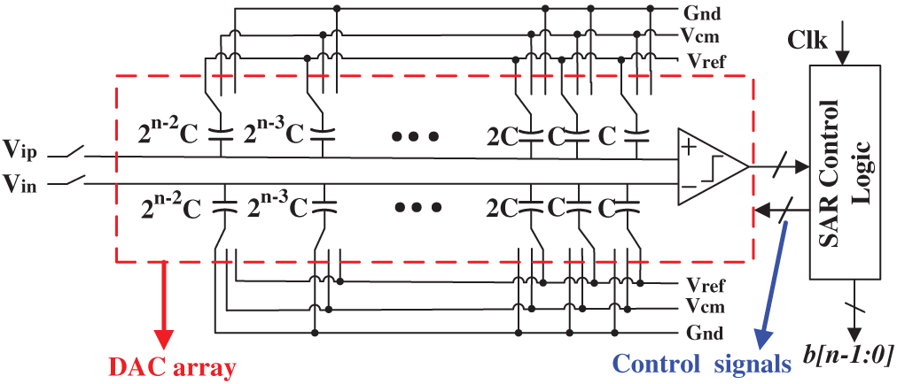
Figure 1: The proposed n-bit SAR ADC architecture
2.1 Analysis of the Proposed Time-Domain Comparator
The proposed time-domain comparator is illustrated in Fig. 2, which is composed of delay cells, two NAND gates, two D-flip-flop register based phase detector and a counter. The operation principle is based on the edge pursuing of two edges originating from two NAND gates similar to [18]. Two flip-flop based register based phase detectors are employed here to judge the polarity of the input. The counter is used to obtain the amount information of the input, which will be used to indicate whether the input is in the predefined window.
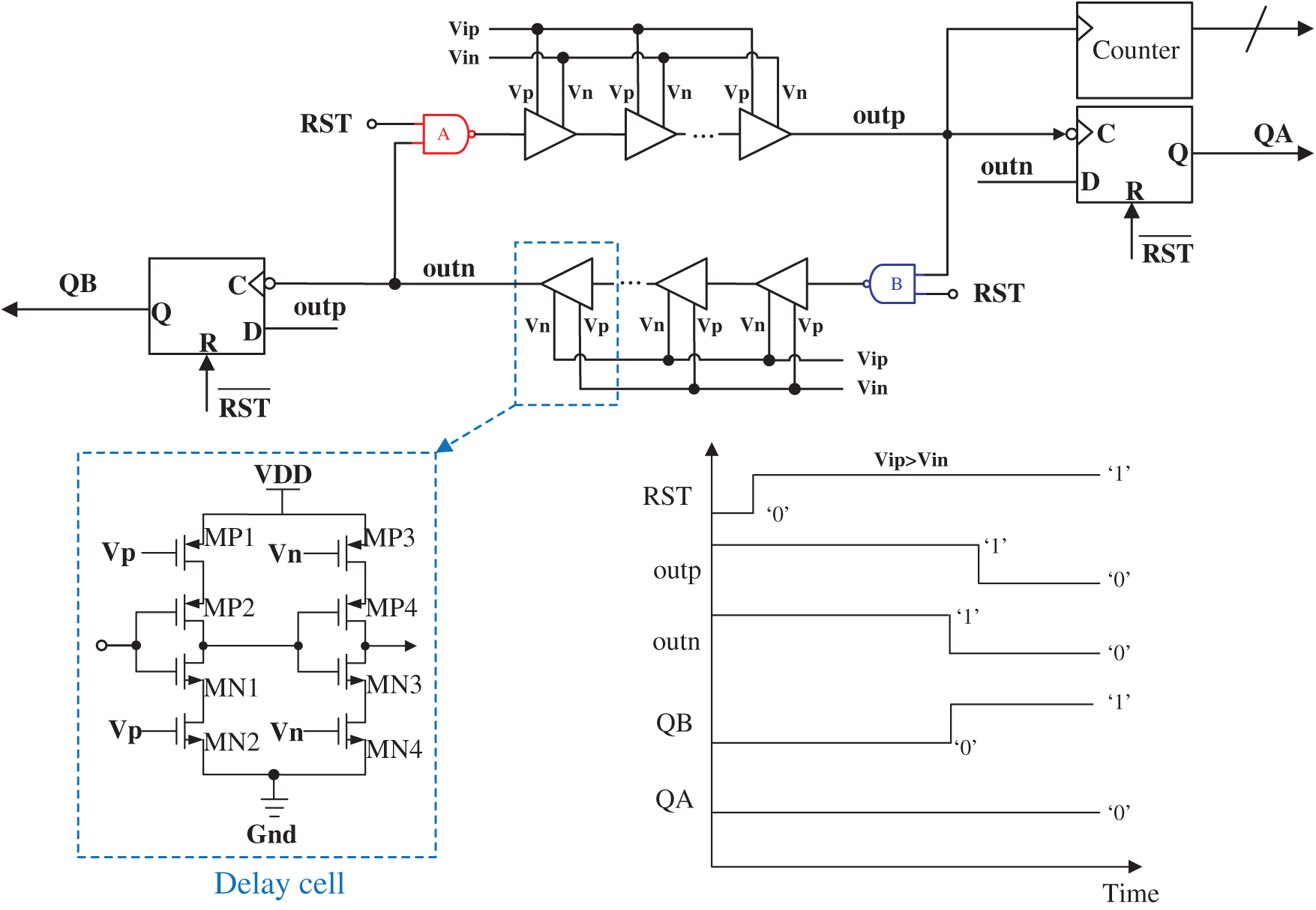
Figure 2: The schematic of the proposed time-domain comparator
Fig. 3 shows the operation principle of the comparator. When RST signal is logic low, the comparator is in reset state. Once RST changes from logic low to logic high, two propagating edges are injected into the oscillator, and travel though the delay cells. The oscillation will stop when one edge overtakes the other one. Fig. 3 illustrates the cases when Vip is larger than Vin but with different amounts. When the voltage difference is small, the two propagating edges have a similar travel speed, and the cycles needed to arrive a decision automatically increase as Fig. 3 shows. On the other hand, if the voltage difference is large, the oscillation will stop very quickly, which inherently reduce the dynamic power consumption. In both cases, outp will settle to 1 (outn will settle to 0 in these cases), which indicates Vip is larger than Vin. Moreover, the oscillation cycles, which is recorded by the counter, can be further utilized to detect the input voltage difference, which facilitates the SAR control logic to improve the whole energy-efficiency of the SAR ADC.
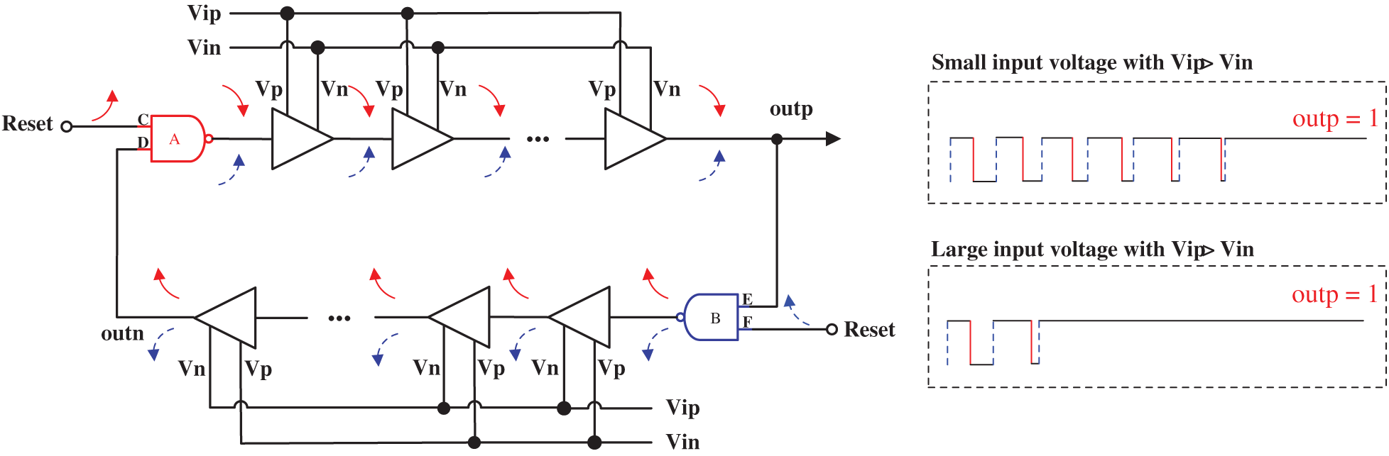
Figure 3: Operation principle of the proposed comparator
The noise root mean square (rms) level
where
2.2 Working Principle of the Skipping-Window
Fig. 4 illustrates the working principle window of the skipping-window. When the SAR ADC powers on, the top plates and the bottom plates of the DAC array are all connected to Vcm. Then the control logic changes the connections of the bottom plates in order to generate the window voltage Vwin. After the DAC settles, the comparator starts to work and the counter number Nwin under Vwin will be recorded. Nwin will be utilized to indicate whether the input voltage falls into the skipping window during the SAR conversion. A SAR conversion will start after the Vwin is set. After the sampling process, the SAR control logic set the current conversion cycle i = 1 and the time-domain comparator compares the DAC output voltages. If the voltage difference is larger than the window voltage Vwin, the SAR control logic will perform the normal SAR conversion cycle by cycle; otherwise, the control logic will judge whether the current conversion cycle i is less than the skipping window cycle Pwin; if i < Pwin, the control logic sets i = Pwin, and perform the rest conversion cycles. Once i >= Pwin, the control logic will perform the normal conversion.
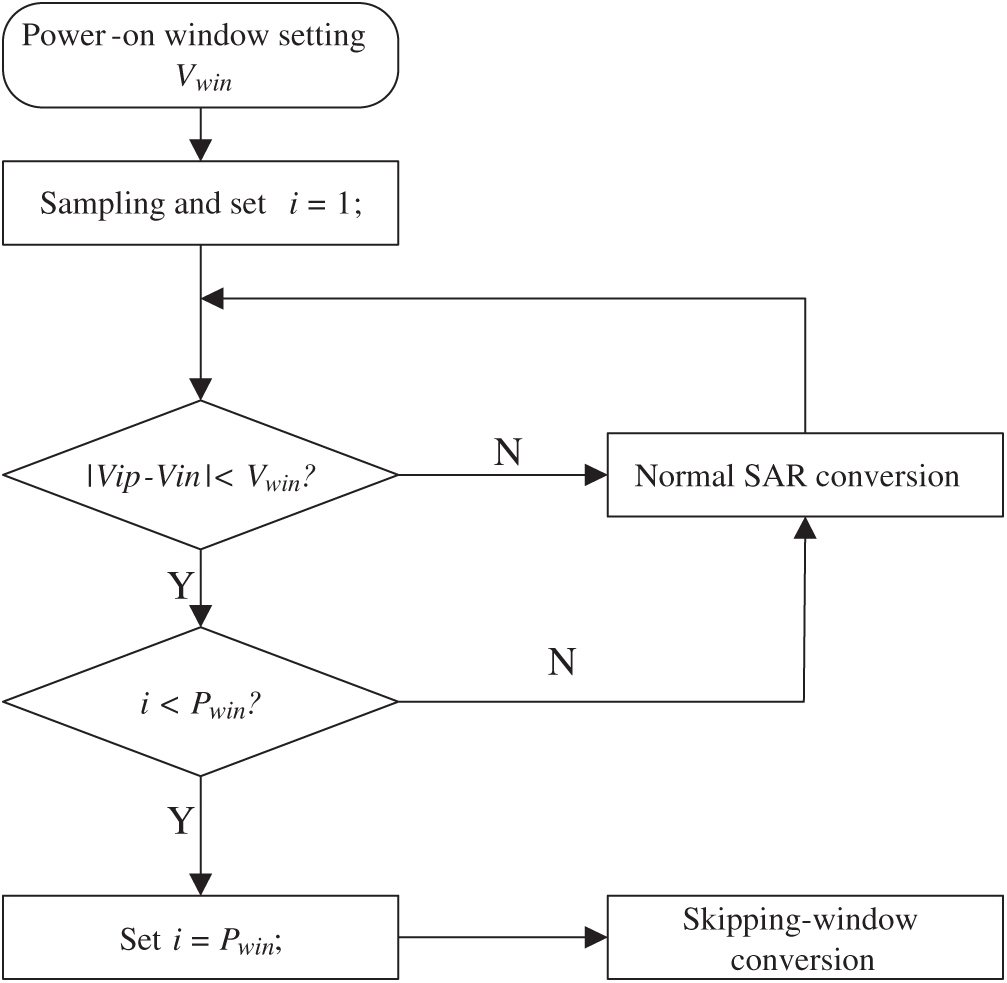
Figure 4: Illustration of the proposed skipping window
Fig. 5 shows the conversion process of a 10-bit SAR ADC model with Vwin = 64 LSBs. The most significant bit (MSB) cycle is denoted as phase 9, and the least significant bit (LSB) cycle is phase 0. Fig. 5a is a normal conversion process and Fig. 5b is a skipping window conversion process. In Fig. 5a, the input voltage difference is larger than Vwin at phase 6, where phase 6 corresponds to the window of 64 LSBs. Thus, no window is skipped for this case. In Fig. 5b, the input falls into the window Vwin at phase 8, the next conversion cycle will skip to phase 5 directly, and two comparison cycles are saved. Thus, when the skipping window triggers, the conversion cycles will reduce, which in turn helps to improve the energy efficiency of the SAR ADC as well as the conversion speed and linearity.
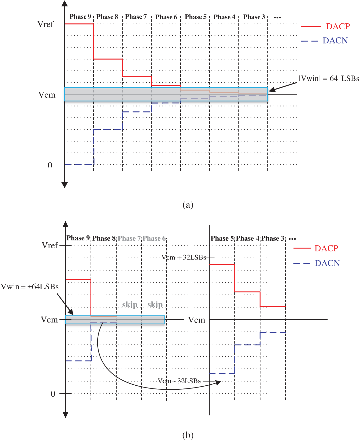
Figure 5: Illustration of the skipping-window scheme with Vwin = 64 LSBs for a 10-bit SAR ADC. (a) Normal conversion. (b) Skipping window conversion
The DAC switching scheme employed here is similar to that used in [14]. No additional switch or capacitor is needed. The skipping window technique is realized by the control logic according to the information provided by the comparator. Fig. 6 gives an example of the proposed skipping size with a window size of 64 LSBs. During the sampling phase, the input is connected to the top plates, and the bottom plates of the DAC array are all connected to the common-mode voltage Vcm, which is represented by ‘1/2’ in Fig. 6. Once the sampling phase is finished, the sampling switches are turned off and the first comparison cycle is carried out directly. According to the comparison results, the control logic judges whether the input difference is less than Vwin. If |Vip − Vin| < Vwin, it means the input voltage is within the voltage window. Under this case, the skipping step is triggered. If Vip > Vin, the bottom plates of
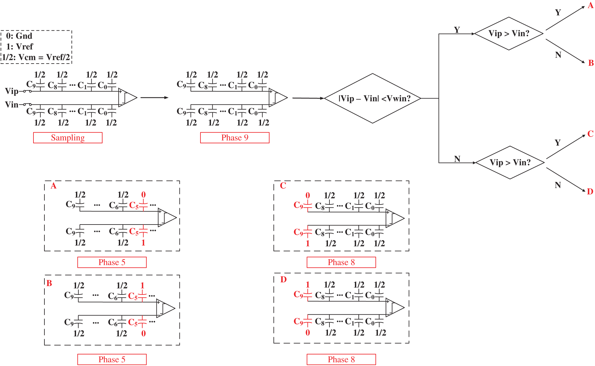
Figure 6: Switching procedure of the DAC with 64 LSBs judge window
3 Analysis of the Skipping Window
3.1 Conversion Cycle Saving for Different Window Size
To prove the efficiency of the proposed skipping window technique when the input falls in the predefined window voltage Vwin, different window voltages are defined to verify the conversion cycle saving. During simulations, a 10-bit SAR ADC model is used. Fig. 7 shows the impact of skipping window size on the percentage of the triggered input. For normal SAR conversion with no skipping window size, all the input will carry out the full conversion cycles, and percentage of the triggered input is 0. When the skipping window size is set to 256 LSBs, the percentage of a full scale input fallen into the skipping window comes to 50%, which can improve the overall energy efficiency of the SAR ADC significantly. When the skipping window size is reduced to 2 LSBs, the percentage is improved to about 99.61%.
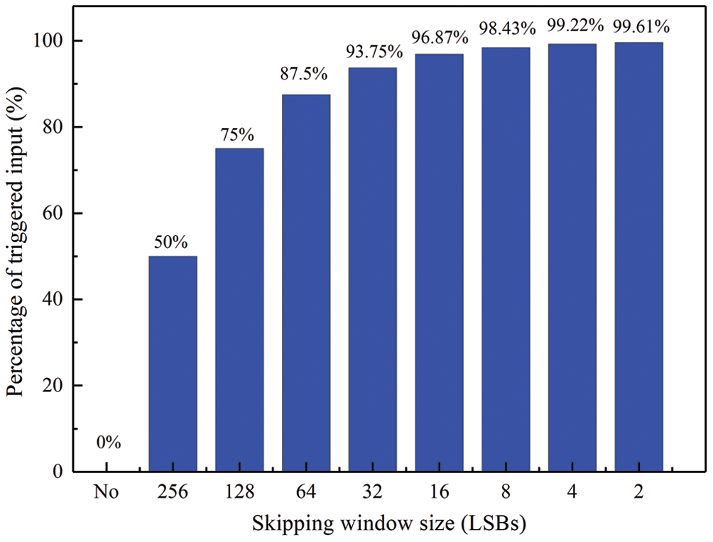
Figure 7: The impact of skipping window size on the percentage of triggered input
3.2 DAC Switching Energy Under Different Window Size
As described in Section 2.2, a large voltage range of the full scale input can fall in the skipping window zone if Vwin is small. However, when Vwin is small, the first MSB cycles can be skipped is less, which results in less energy efficiency of DAC. In order to evaluate the effect of the skipping window size on the DAC switching energy, a 10-bit SAR ADC model with the merged capacitor switching (MCS) scheme in [14] is employed. Fig. 8 shows the DAC switching energy under different skipping window size. It is clearly that when the skipping window size is large, the DAC consumes less switching energy than those with small skipping window sizes. This is because when the window size is large, most MSB cycles can be skipped. As the first few MSB conversion cycles occupies a large amount of the overall DAC switching energy, when the window size is large, the probability of the first few MSB conversion cycles will be skipped is high.
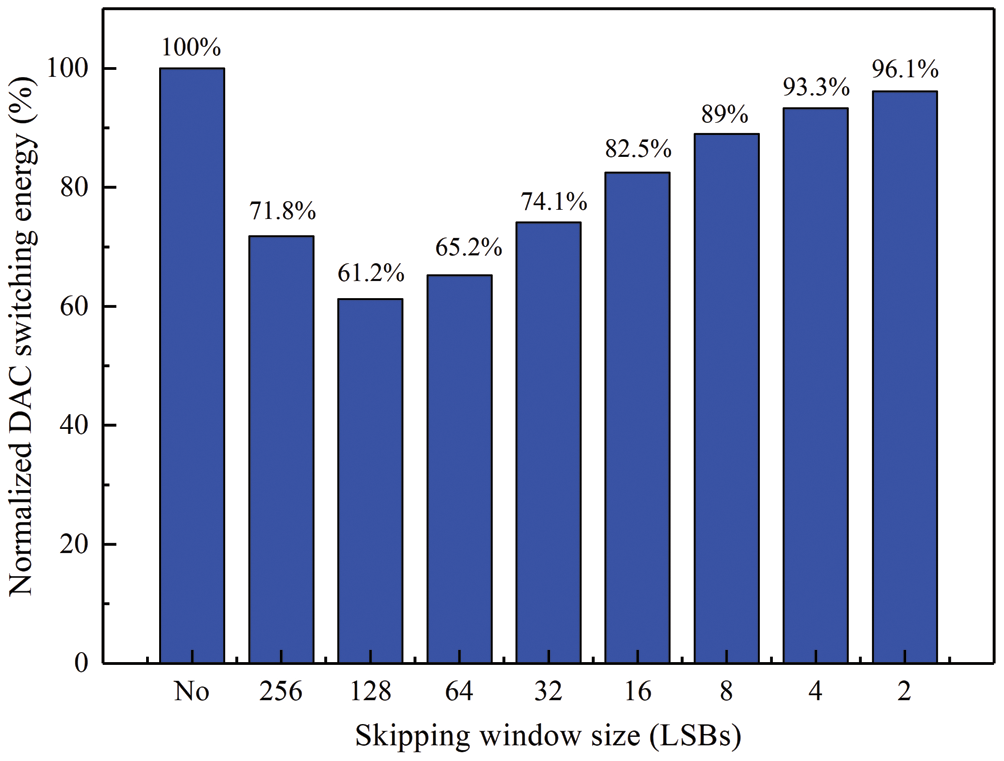
Figure 8: The impact of skipping window size on DAC switching energy
3.3 Overall Power Saving for Different Window Size
In SAR ADC, most of the power is consumed by three main building blocks, including comparator, DAC capacitor arrays and control logic. Since the DAC switching energy is not the same for different cycles during a conversion, the energy saving with different window size can be evaluated by supposing that each output code has the same probability, and the average DAC switching energy is denoted as EDAC. For simplicity, we assume that the power consumption for the comparator Ecomp and the control logic Edig do not change for each bit-cycle.
For a normal conversion cycle, the power consumption for the comparator and the control logic are
where
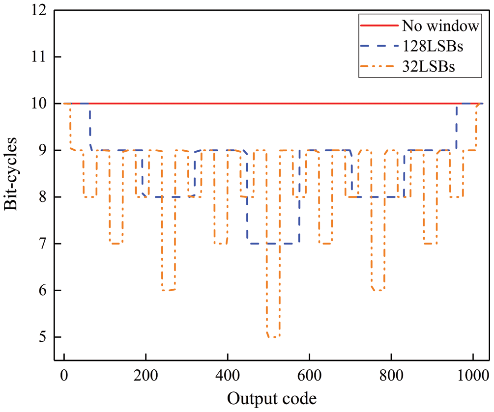
Figure 9: Bit-cycles against output code under different window size
In order to evaluate the performance of the proposed skipping window technique, a 10-bit SAR ADC model is used. During simulations, the power consumption of the comparator and the control logic is assumed unchanged for each bit-cycle. Fig. 10 shows the switching energy against the output under different window size. The proposed skipping window technique can improve the DAC switching energy effectively. When the window size is 128 LSBs, the DAC energy saving is 38.8% compared to that of with no window.
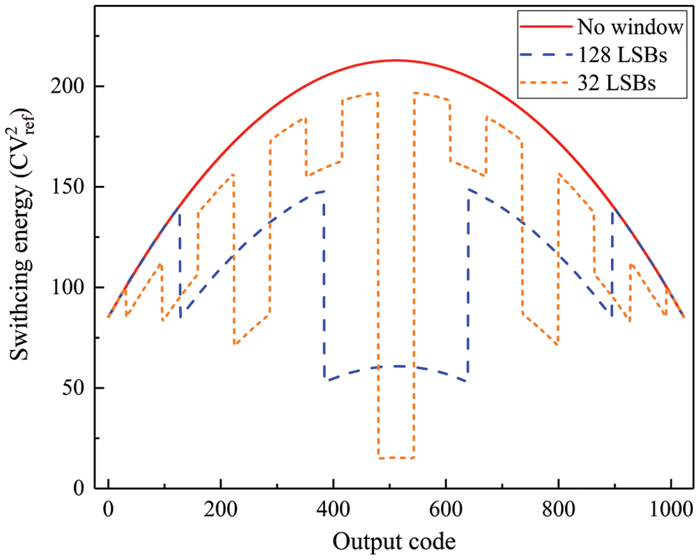
Figure 10: Switching energy against output code under different window size
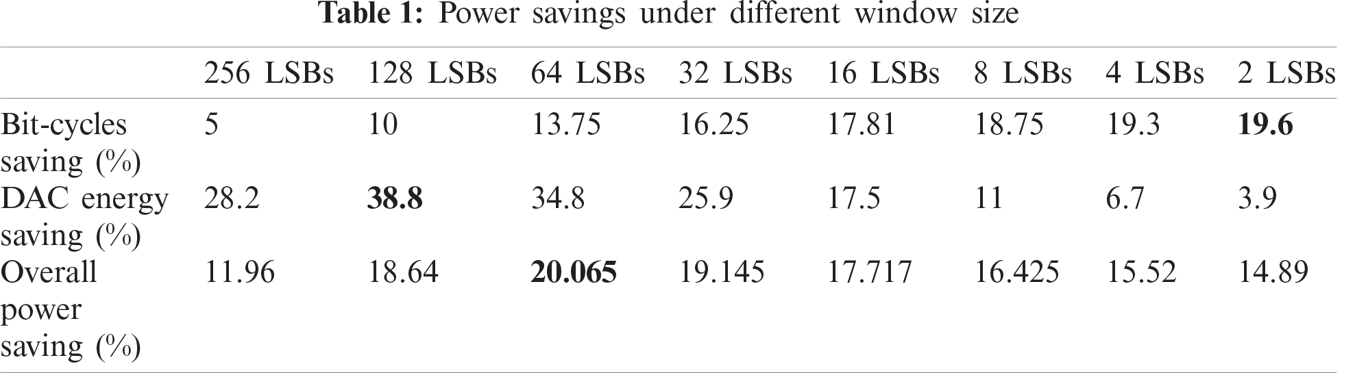
Fig. 11 shows the static performance of the SAR ADC under different window size. The skipping-window technique can reduce the non-linearity of the DAC effectively, that is because the skipping process triggered by the window can reduce the accumulated error caused by the capacitor mismatch. Tab. 1 summaries the power savings under different window size. Here, it is assumed that each output code has the same probability, the power consumption of the comparator and the control logic is 70% and the DAC occupies the rest 30% of the whole SAR ADC. For a 10-bit SAR ADC, there are 1024 output codes, and each code needs 10 bit-cycles for traditional SAR conversion, and 10240 bit-cycles are required in total. The bit-cycles saving is the saved bit-cycles over the total bit-cycles. Although a small window size can save more bit-cycles, the DAC energy saving is less, which results in less energy-efficient for the whole SAR ADC. For the DAC energy saving, 128 LSBs window size is the most energy-efficient one. When it comes to the overall power saving, the window size with 64 LSBs is the best choice. It should be noted that the MCS scheme in [14] is employed and 30% power consumption for the DAC is assumed during simulations. If the DAC switching scheme or the power consumption for the DAC varies, the optimized window size may be different.
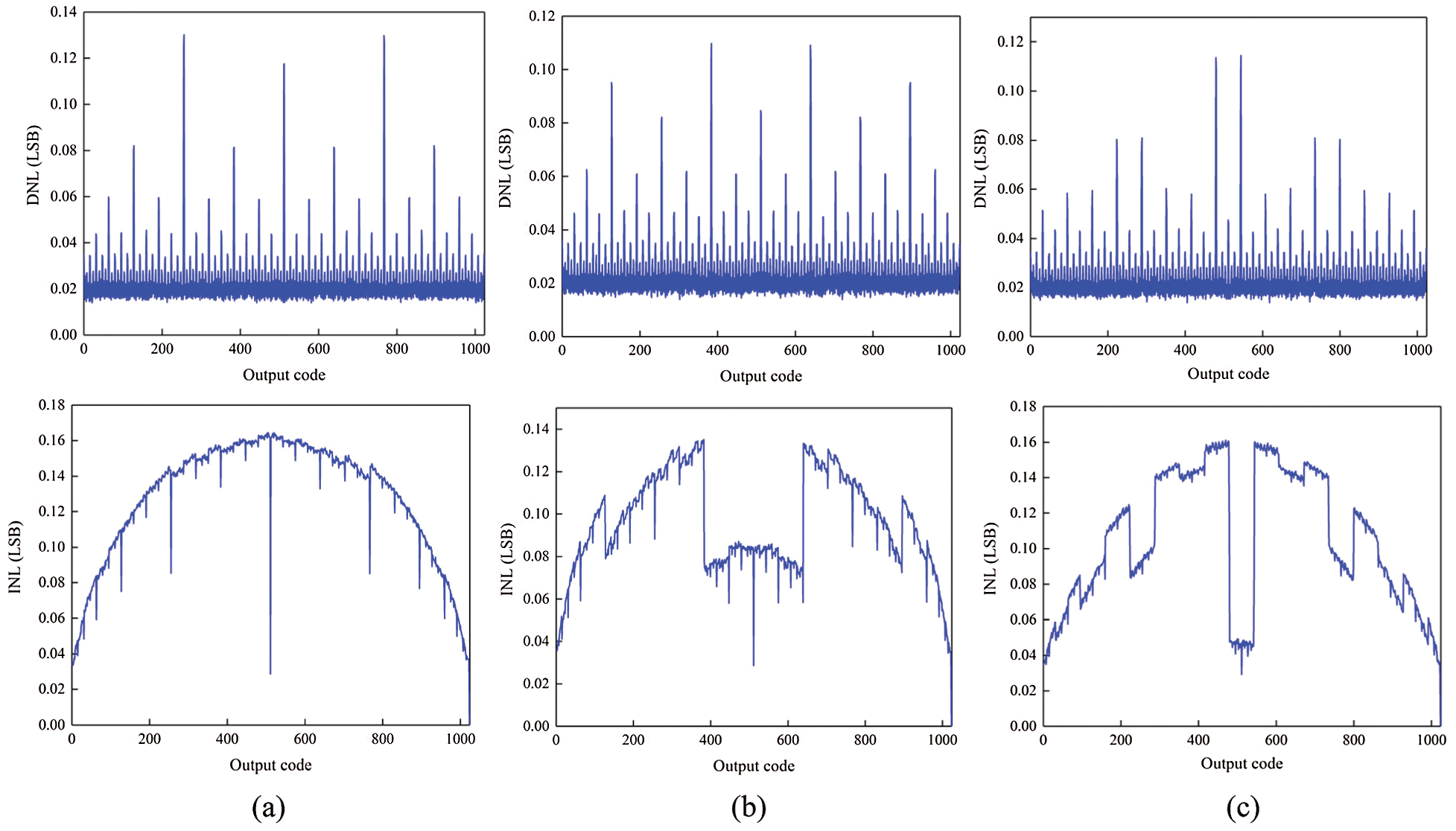
Figure 11: Static performance with different window size: (a) No window, (b) 128 LSBs, (c) 32 LSBs
A SAR ADC with skipping window is presented. The proposed comparator provides not only the polarity information of the input, but also the amount of the input difference, which is employed to indicate the window voltage. The window voltage can be easily adjusted by connecting different DAC capacitors to corresponding reference voltages. The impacts on the DAC switching power and the conversion cycles are analyzed. Simulation results show that the proposed skipping window can effectively improve the overall energy-efficiency of SAR ADC.
Funding Statement: This work was supported partly by the National Natural Science Foundation of China under Grant No. 61704015, and the General program of Chongqing Natural Science Foundation (a special program for the fundamental and frontier research) under Grant No. cstc2019jcyj-msxmX0108.
Conflicts of Interest: The authors declare that they have no conflicts of interest to report regarding the present study.
1. D. Zhu, Y. Sun, H. Du, N. Cao, T. Baker et al., “HUNA: A method of hierarchical unsupervised network alignment for IoT,” IEEE Internet of Things Journal, vol. 8, no. 5, pp. 3201–3210, 2021. [Google Scholar]
2. S. K. Kim, M. Köppen, A. K. Bashir and Y. Jin, “Advanced ICT and IOT technologies for the fourth industrial revolution,” Intelligent Automation & Soft Computing, vol. 26, no. 1, pp. 83–85, 2020. [Google Scholar]
3. D. Kim, S. D. Min and S. Kim, “A DPN (delegated proof of node) mechanism for secure data transmission in IoT services,” Computers, Materials & Continua, vol. 60, no. 1, pp. 1–14, 2019. [Google Scholar]
4. C. Liu, S. Chang, G. Huang and Y. Lin, “A 0.92 mW 10-bit 50-MS/s SAR ADC in 0.13 μm CMOS process,” in Symp. on VLSI Circuits, Kyoto, Japan, pp. 236–237, 2009. [Google Scholar]
5. X. Wang, X. Zhou and Q. Li, “A high-speed energy-efficient segmented prequantize and bypass DAC for SAR ADCs,” IEEE Transactions on Circuits and Systems II: Express Briefs, vol. 62, no. 8, pp. 756–760, 2015. [Google Scholar]
6. T. Yousefi, A. Dabbaghian and M. Yavari, “An energy-efficient DAC switching method for SAR ADCs,” IEEE Transactions on Circuits and Systems II: Express Briefs, vol. 65, no. 1, pp. 41–45, 2017. [Google Scholar]
7. Y. H. Chung, C. W. Yen and M. H. Wu, “A 24-μW 12-bit 1-MS/s SAR ADC with two-step decision DAC switching in 110-nm CMOS,” IEEE Transactions on Very Large Scale Integration (VLSI) Systems, vol. 24, no. 11, pp. 3334–3344, 2016. [Google Scholar]
8. W. Mao, Y. Li, C. H. Heng and Y. Lian, “A low power 12-bit 1-kS/s SAR ADC for biomedical signal processing,” IEEE Transactions on Circuits and Systems I: Regular Papers, vol. 66, no. 2, pp. 477–488, 2018. [Google Scholar]
9. S. E. Hsieh and C. C. Hsieh, “A 0.3-V 0.705-fJ/conversion-step 10-bit SAR ADC with a shifted monotonic switching procedure in 90-nm CMOS,” IEEE Transactions on Circuits and Systems II: Express Briefs, vol. 63, no. 12, pp. 1171–1175, 2016. [Google Scholar]
10. K. T. Lin, Y. W. Cheng and K. T. Tang, “A 0.5 V 1.28-MS/s 4.68-fJ/conversion-step SAR ADC with energy-efficient DAC and trilevel switching scheme,” IEEE Transactions on Very Large Scale Integration (VLSI) Systems, vol. 24, no. 4, pp. 1441–1449, 2015. [Google Scholar]
11. A. Agnes, E. Bonizzoni, P. Malcovati and F. Maloberti, “A 9.4-ENOB 1V 3.8 μW 100kS/s SAR ADC with time-domain comparator,” in IEEE Int. Solid–State Circuits Conf.-Digest of Technical Papers, San Francisco, CA, pp. 246–610, 2008. [Google Scholar]
12. S. Rout, S. Babayan-Mashhadi and W. A. Serdijn, “A subthreshold source-coupled logic based time-domain comparator for SAR ADC based cardiac front-ends,” in IEEE Asia Pacific Conf. on Circuits and Systems, Bangkok, Thailand, pp. 17–20, 2019. [Google Scholar]
13. C. Kao, S. Hsieh and C. Hsieh, “A 0.5 V 12-bit SAR ADC using adaptive time domain comparator with noise optimization,” in IEEE Asian Solid-State Circuits Conf., Seoul, pp. 213–216, 2017. [Google Scholar]
14. V. Hariprasath, J. Guerber, S. H. Lee and U. K. Moon, “Merged capacitor switching based SAR ADC with highest switching energy-efficiency,” Electronics Letters, vol. 46, no. 9, pp. 620–621, 2010. [Google Scholar]
15. C. Yuan and Y. Lam, “Low-energy and area-efficient tri-level switching scheme for SAR ADC,” Electronics Letters, vol. 48, no. 9, pp. 482–483, 2012. [Google Scholar]
16. X. Song, Y. Xiao and Z. Zhu, “VCM-based monotonic capacitor switching scheme for SAR ADC,” Electronics Letters, vol. 49, no. 5, pp. 327–328, 2013. [Google Scholar]
17. Y. Song, Z. Xue, Y. Xie, S. Fan and L. Geng, “A 0.6-V 10-bit 200-kS/s fully differential SAR ADC with incremental converting algorithm for energy efficient applications,” IEEE Transactions on Circuits and Systems I: Regular Papers, vol. 63, no. 4, pp. 449–458, 2016. [Google Scholar]
18. M. Shim, S. Jeong, P. D. Myers, S. Bang, J. Shen et al., “Edge-pursuit comparator: An energy-scalable oscillator collapse-based comparator with application in a 74.1 dB SNDR and 20 kS/s 15 b SAR ADC,” IEEE Journal of Solid-State Circuits, vol. 52, no. 4, pp. 1077–1090, 2017. [Google Scholar]
19. Z. Ding, X. Zhou and Q. Li, “A 0.5-1.1-V adaptive bypassing SAR ADC utilizing the oscillation-cycle information of a VCO-based comparator,” IEEE Journal of Solid-State Circuits, vol. 54, no. 4, pp. 968–977, 2019. [Google Scholar]
20. S. Chang, X. Zhou, Z. Ding and Q. Li, “A 12-bit 30 MS/s SAR ADC with VCO-based comparator and split-and-recombination redundancy for bypass logic,” in 2019 IEEE Int. Symp. on Circuits and Systems, Sapporo, Japan, pp. 1–5, 2019. [Google Scholar]
21. G. Y. Huang, S. J. Chang, C. C. Liu and Y. Z. Lin, “A 1-μW 10-bit 200-kS/s SAR ADC with a bypass window for biomedical applications,” IEEE Journal of Solid-State Circuits, vol. 47, no. 11, pp. 2783–2795, 2012. [Google Scholar]
22. Y. H. Chung, C. W. Yen, P. K. Tsai and B. W. Chen, “A 12-bit 40-MS/s SAR ADC with a fast-binary-window DAC switching scheme,” IEEE Transactions on Very Large Scale Integration Systems, vol. 26, no. 10, pp. 1989–1998, 2018. [Google Scholar]
23. Y. H. Chung, Q. F. Zeng and Y. S. Lin, “A 12-bit SAR ADC with a DAC-configurable window switching scheme,” IEEE Transactions on Circuits and Systems I: Regular Papers, vol. 67, no. 2, pp. 358–368, 2019. [Google Scholar]
 | This work is licensed under a Creative Commons Attribution 4.0 International License, which permits unrestricted use, distribution, and reproduction in any medium, provided the original work is properly cited. |