DOI:10.32604/cmc.2021.016811
| Computers, Materials & Continua DOI:10.32604/cmc.2021.016811 | |
| Article |
Reconfigurable Compact Wideband Circularly Polarised Dielectric Resonator Antenna for Wireless Applications
1LCOMS, ASEC, University de Lorraine, Metz, 57070, France
2School of Physics and Electronic Information, Yanan Univeristy, Yanan, 761000, China
3Department of Electronics Technology, University of Technology, Nowshera, 24100, Pakistan
4Department of Electrical Engineering, National University of Sciences and Technology, Islamabad, 44000, Pakistan
5Department of Computer Systems Engineering, University of Engineering and Technology, Peshawar, 25120, Pakistan
6Department of Electronic Engineering, The Islamia University of Bahawalpur, Bahawalpur, 63100, Pakistan
*Corresponding Author: Shahid Khan. Email: Shahid.khan@univ-lorraine.fr
Received: 12 January 2021; Accepted: 20 February 2021
Abstract: In this work, a novel compact wideband reconfigurable circularly polarised (CP) dielectric resonator antenna (DRA) is presented. The L-shaped Dielectric resonator antenna is excited by an inverted question mark shaped feed. This arrangement of feed-line helps to generate two orthogonal modes inside the DR, which makes the design circularly polarised. A thin micro-strip line placed on the defected ground plane not only helps to generate a wideband response but also assist in the positioning of the two diode switches. These switches located at the left and right of the micro-strip line helps in performing two switching operations. The novel compact design offers the reconfigurability between 2.9–3.8 GHz which can be used for different important wireless applications. For the switching operation I, the achieved impedance bandwidth is 24% while axial ratio bandwidth (ARBW) is 42%. For this switching state, the design has 100% CP performance. Similarly, the switching operation II achieves 60% impedance bandwidth and 58.88% ARBW with 76.36% CP performance. The proposed design has a maximum measured gain of 3.4 dBi and 93% radiation efficiency. The proposed design is novel in terms of compactness and performance parameters. The prototype is fabricated for the performance analysis which shows that the simulated and measured results are in close agreement.
Keywords: Circularly polarized; DRA; ARBW; bandwidth; gain; radiation efficiency
Dielectric Resonator Antennas (DRAs) are recently getting more attention. They have a number of additional advantages over conventional microstrip patch antennas (MPAs) which includes non-metallic structure, wide impedance bandwidth, high gain and radiation efficiency [1]. Due to their 3D structure, DRs can be excited with a number of feeding options and each feeding mechanism is helpful in generating a different response. Conventional MPAs due to their metallic structure and skin effect, offer losses which effect their radiation efficiency and operating bandwidth [2].
Designing multiband antennas for a range of wireless applications is a very useful technique but due to bandwidth scarcity, the unused resonance frequencies of these designs reduce their usefulness [3,4]. In this situation, the significance of the reconfigurable DRAs increases two folds as they give more freedom to use the bandwidth efficiently with good performance parameters.
Recently, reconfigurable or multi-functional DRAs have gained more attention. They have highly reduced the design complexity, as single design has the potential to perform a number of tasks. For 4G and 5G communication systems, reconfigurable DRAs are preferred as they reduce the overall size and price of the devices. Numerous designs which include wide band reconfigurable DRAs, narrow band reconfigurable DRAs, wide to narrow band reconfigurable DRAs, pattern and frequency reconfigurable DRAs have been widely studied in the literature [5]. To perform the reconfigurability, different techniques can be incorporated [6]. These different techniques alter the current distribution in the DRs which change the operating modes and resonance frequencies [7]. Compact wideband reconfigurable circularly polarised DRAs are even more useful in multi-path loss environments, rainy season, high terrain and buildings [8]. They are also good candidates for the satellite and RADAR communication [2]. Designing such type of DRAs are very challenging, as achieving four features simultaneously require a number of techniques in a single design [9–11].
In the available literature, either we find wideband CP DRAs without reconfigurability or reconfigurable DRAs without being circularly polarised. Moreover, these designs suffer from the compactness issues as well. In [12] frequency reconfigurable DR is discussed. The DR is neither compact and nor circularly polarized which highly decreases its usefulness. In [13] a wideband circularly polarised DRA is presented. This design does not perform reconfigurability and the size of the DR is bulky for the wireless devices. In [14] a reconfigurable hybrid CP DRA is discussed in detail. The proposed design has some good results but DR thickness and low CP performance degrade its significance. In [15] a reconfigurable dual/triple band CP DRA is presented. The proposed design has probe feeding with very complex structure, large volume and low performance. Designing a wideband, compact and reconfigurable circularly polarised DRA is very challenging and so far, no significant work has been done on compact wideband reconfigurable circularly polarized DRAs. Some work done on planar DRAs are mostly linear [5,6]. This factor motivated us to work on compact wideband reconfigurable circularly polarized DRA design. The design is novel in three aspects. First, it is very compact with 2 mm DR thickness only. Secondly, the response is wideband with 100% and 76.36% CP performance for both the switching configurations which is never achieved before. Thirdly the design is very simple with the potential of wide bandwidth and circular polarization reconfigurability simultaneously. It was very challenging to achieve these characteristics. By incorporating special design procedures and proper optimization techniques helped to achieve the required results.
In this work, an L-shaped wideband compact circularly polarized reconfigurable DRA antenna is presented in detail. The design generates CP fields with the help of an inverted question mark shaped feed-line, as it excites two orthogonal modes from two different sides of the DR. The Wide-band operation and compact size is achieved due to the introduction of the defective ground structure (DGS) [5]. In order to improve the reflection coefficient and to introduce a slight shift in the bandwidth, a small portion of the rectangular DR is removed which makes the DR L-shaped. Introducing parasitic micro-strip line on the defective ground structure helps in shifting the resonance frequencies and also in the positioning of the two diodes. Two diodes (model BAR-50-02 V) which act as RF switches are located to the extreme left and right of the parasitic micro-strip line which provide two possible switching arrangements. These switches connect and disconnect the parasitic micro-strip line with the ground plane on the left and right side. These two switching arrangements reconfigure both the resonance frequencies and their corresponding axial ratios. The impedance bandwidth for the OFF-ON switching state is 24% with full CP (100%) performance within the whole bandwidth. For the ON-OFF state, the operating bandwidth and ARBW get widen. The operating bandwidth is about 60% with 76.36% CP performance for the whole band. The proposed design has a maximum gain of 3 dBi and 93% radiation efficiency.
Fig. 1 illustrates the detail of the proposed design. The proposed design is based on a slot in the ground and a rectangular DR with relative permittivity of 30.0 and dimensions of
where fr is the resonance frequency of the design, C is the speed of light and Kx, Ky and Kz are the wave numbers in x, y and z direction. L, W and H are the length, width and height of the DR respectively. The DR is positioned on the FR4 substrate which has 4.2 relative permittivity and 0.002 tangent loss. The ground has a rectangular slot, thus high permittivity of the DR and a wide rectangular slot collectively makes the DR very compact with just 2 mm thickness. The DR is fed with a 50
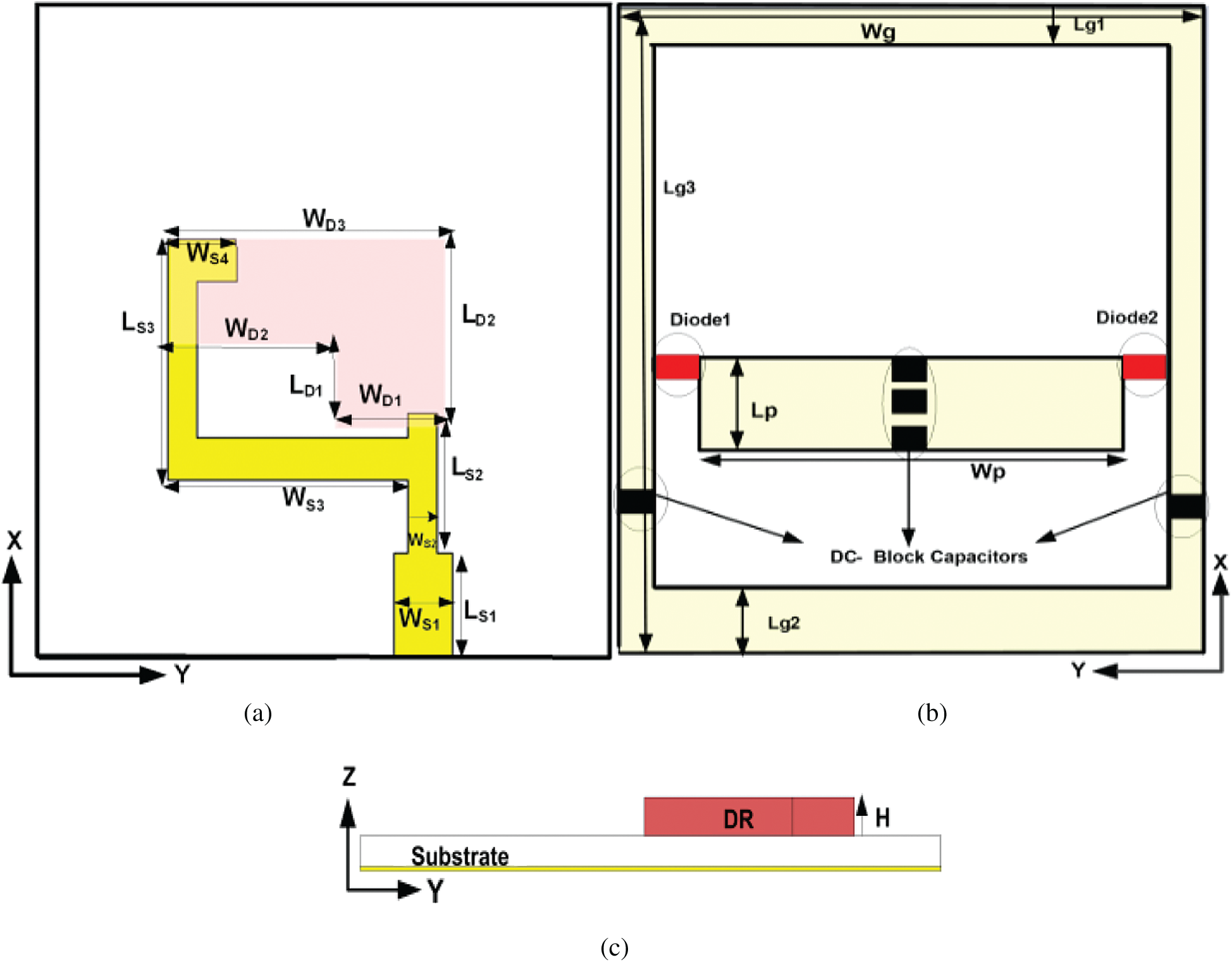
Figure 1: (a) Front view, (b) bottom view and (c) side view
Fig. 1b shows the bottom view of the proposed CP DRA. A parasitic metallic strip on the bottom side of the substrate results in improving the impedance bandwidth and axial ratio. This parasitic strip on the bottom side of the substrate has maximum effect when positioned just below the lower side of the DR. This way it covers half of the DR and produces maximum effect. It also assists to locate the two PIN Diodes at the left and right sides, which perform the reconfigurability. The introduction of the strip on the rectangular etched slot plays an important role in reconfiguring the resonance frequency and axial ratio. On the same side of the substrate, few DC block capacitors (22 pF each) are also introduced. Two capacitors are placed on the ground plane while three others are positioned on the parasitic strip line as shown in Fig. 1b. The capacitors block the DC current flow into the RF feed-line during diode biasing. Fig. 1c shows the side view of the design. It can be seen from the Fig. 1c that the proposed design is compact with only 2 mm height of the DR. The detail of the different dimensions of the proposed design is summarised in the Tab. 1.
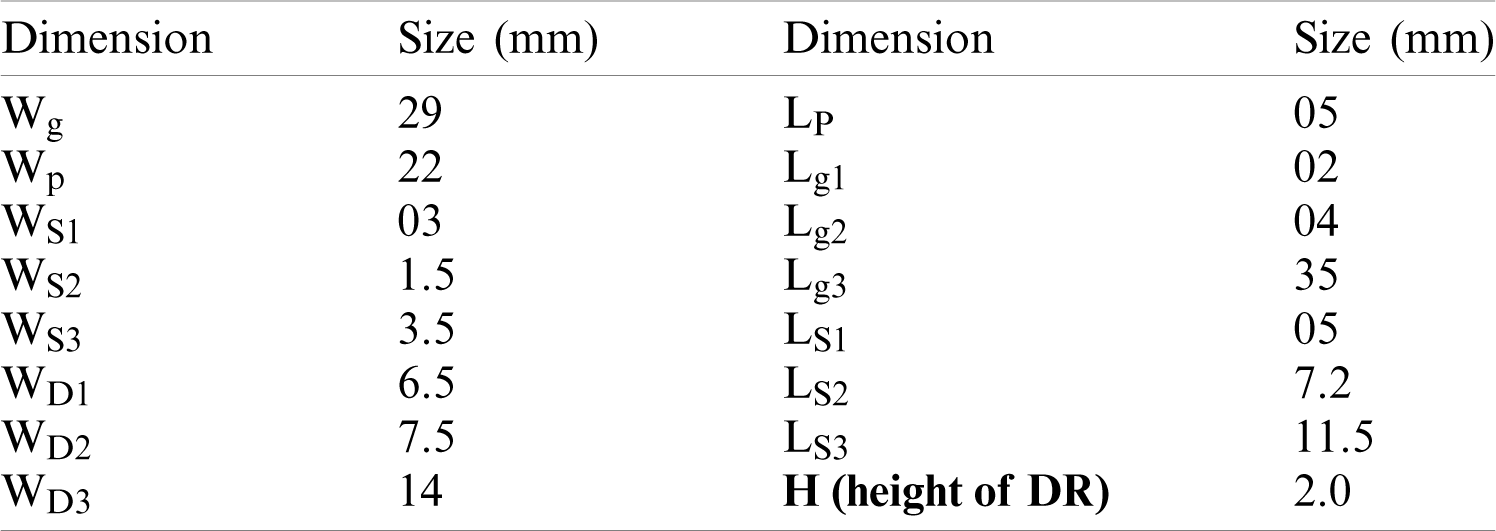
Table 1: Dimensions and related parameters of L-shaped patch and array structure
Stepwise design procedure is explained in Fig. 2. The corresponding reflection coefficient and axial ratio for each step is shown in Figs. 3 and 4 respectively.
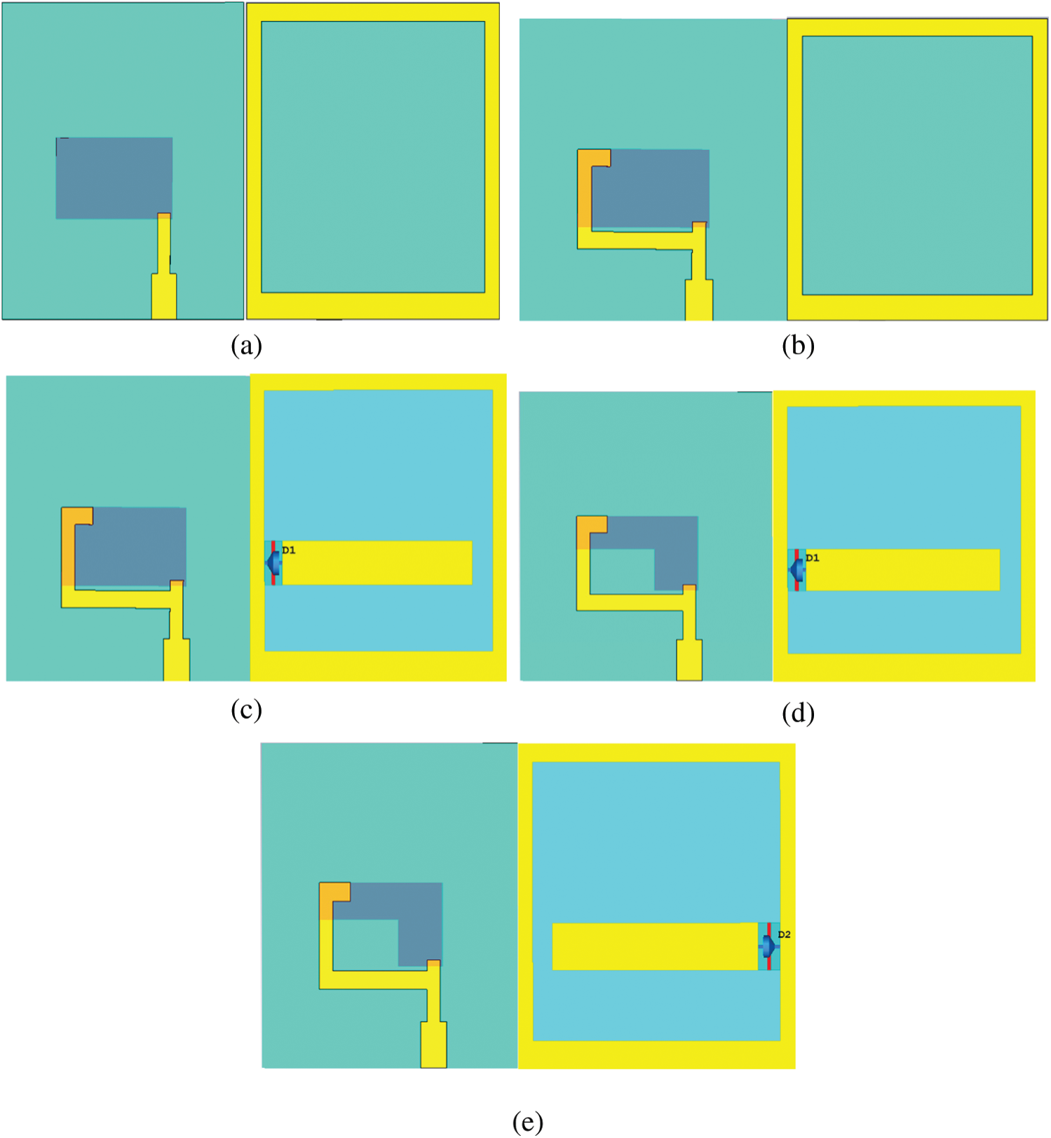
Figure 2: Stepwise design evaluation of the design. (a) Design A is step 1, (b) Design B is step 2, (c) Design C is step 3, (d) Design D is step 4 and (e) Design E is the last step.
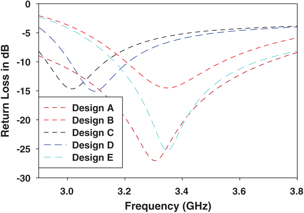
Figure 3: Return loss for different evolution steps
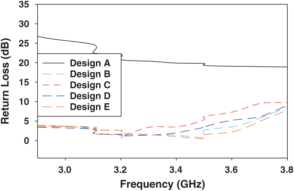
Figure 4: Axial ratio for different evolution steps
The proposed design evolution starts with a rectangular DR positioned on the top surface of the substrate. This DR is accompanied by the defective ground with a rectangular slot as shown in Design A. This rectangular slot along with high permittivity of the DR helps to make the design very compact. Fig. 3 shows that the Design A give a wideband response with 3.3 GHz resonance frequency. Fig. 4 shows that Design A has no circular polarization. In step two as shown in Design (b), the feedline is extended to other side of the DR. Fig. 3 shows that extension of the feedline makes the design slightly mismatched which effects the reflection coefficient but on the other side it highly improves the axial ratio and make the design circularly polarized. Although design (b) is circularly polarized but it does not over the maximum target operating band. To cover the maximum operating from 3 to 3.8 GHz, a small parasitic strip is introduced. As clear from design (c) the parasitic strip on the bottom surface of the substrate is connected with the ground by a PIN diode. This shift both the operating band and axial ratio to low frequencies but the overlapping bandwidth and axial ratio are minimum. To maximize the overlapping bandwidth and axial ratio, a rectangular cut is introduced into the DR. This rectangular cut shifts the bandwidth towards high frequencies while have no impact on axial ratio. To reconfigure the frequency and axial ratio, another RF switch (PIN diode) is connected to the right of the parasitic strip. Figs. 3 and 4 shows that when D1 is OFF and D2 is ON the operating band and axial ratio shifts to high frequency. Thus, the overall design with the help of two switching operations cover the maximum operating bandwidth.
A number of parameters contribute to finalize the design. Amongst these important parameters, relative permittivity of the DR, the cut section of the DR and width of the parasitic strip highly effect the overall performance generally and specifically return loss and axial ratio. Figs. 5 and 6 shows the effect of the changing the relative permittivity of the DR on the bandwidth and axial ratio without changing the DR size. With the increase in the DR relative permittivity, the operating bandwidth shifts to lower frequencies [16]. Correspondingly, axial ratio shows improvement with the increase in the relative permittivity [17]. The required shift in resonance frequency and improvement in the axial ratio is achieved when DR relative permittivity is kept 30.
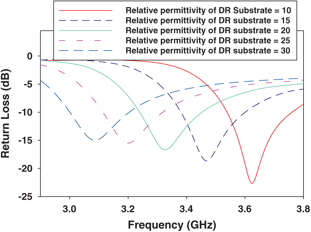
Figure 5: Effect of DR permittivity on bandwidth
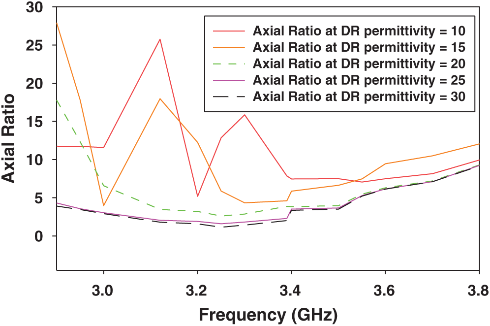
Figure 6: Effect of DR permittivity on axial ratio
Similarly, rectangular cut which is introduced by removing some portion of the DR helps to shift the bandwidth towards the high frequencies [18]. Moreover, with this, the compact design is further miniaturized. As shown in Fig. 7 the target shift is achieved with DR cut of 9 mm in width. The reason behind shifting the resonance frequency is to achieve maximum overlapping bandwidth with the axial ratio. Additionally, from the simulated results it is also observed that DR cut has minimum impact on the axial ratio and no major shift or change is noticed.
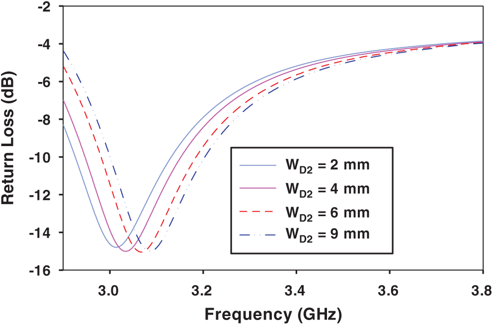
Figure 7: Effect of DR cutting on return loss
Figs. 8 and 9 show the impact of varying parasitic metallic strip thickness on the return loss and axial ratio. Parasitic metallic strip located on the bottom side of the substrate highly effect the return loss and axial ratio [19,20]. The increasing width of the parasitic strip improve the impedance matching which in result improve the return loss and increases the bandwidth but on other side, it degrades the axial ratio [21]. The possible reason is the width of the parasitic strip which improves the impedance matching but disturb the current distribution of two orthogonal mode generated inside the DR by inverted question mark shaped feed line. This degrades the axial ratio. The maximum width of the parasitic strip is kept 7 mm. This much width of the parasitic strip covers lower half of the DR, thus give very good value of axial ratio and acceptable values of the return loss.
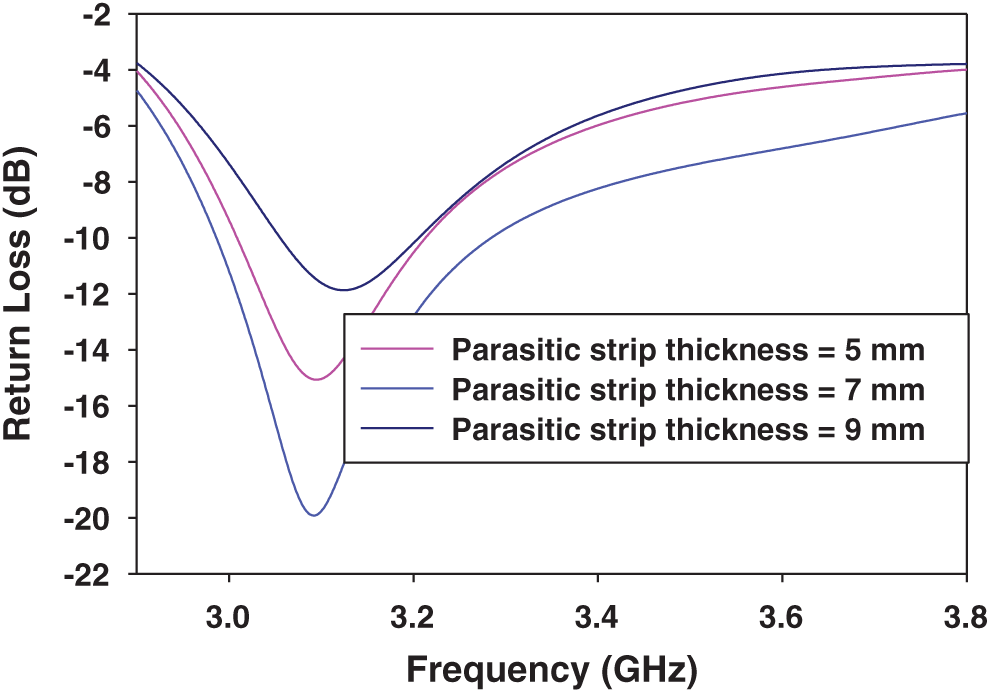
Figure 8: Effect of varying parasitic strip thickness on return loss
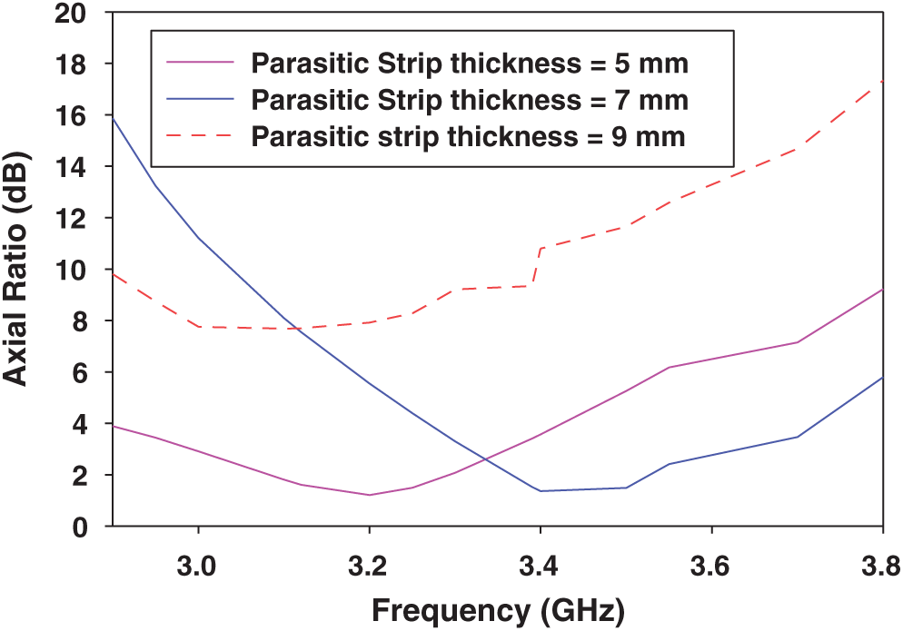
Figure 9: Effect of varying parasitic strip on axial ratio
5 Surface Current Distribution
Figs. 10 and 11 show the current distribution on the upper surface of the DRA in OFF-ON and ON-OFF state. The E-field distribution at 3.1 and 3.37 GHz is confirmed at
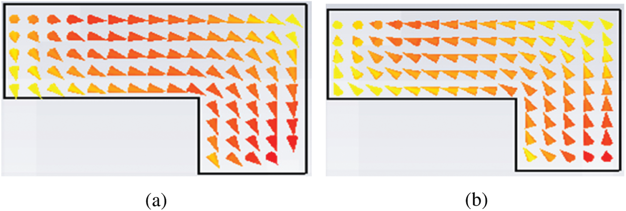
Figure 10: E-field distribution on the upper surface of the DRA. (a) 3.1 GHz at 0
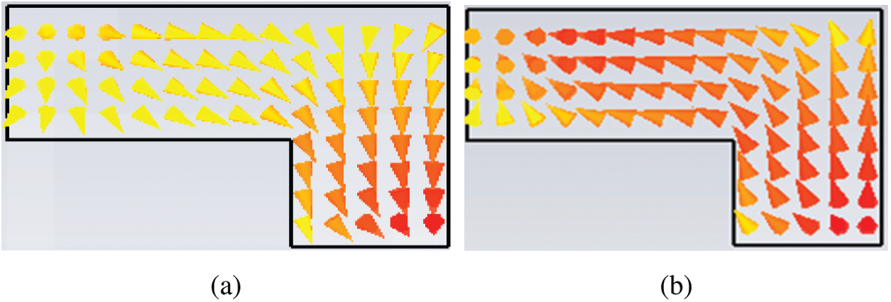
Figure 11: E-field distribution on the upper surface of the DRA. (a) 3.37 GHz at 0
To confirm the accuracy and results of the simulated structure, the proposed design is fabricated on FR4 epoxy substrate with 1.6 mm thickness. An L-shaped DR of 2 mm thickness is mounted on the top surface of the substrate. Two PIN diodes are placed to the left and right of the parasitic strip. To block the flow of DC current into the RF feedline, three capacitors are placed in the mid of the parasitic strip while other two capacitors are placed on the ground [22]. An alternative can be RF chokes but due to easy availability and low price, capacitors are preferred. In this section important antenna results which include reflection coefficient (return loss), radiation pattern and gain of the proposed design is discussed in detail. Moreover, comparison of the proposed with the recently published state of the art work is also presented in this work. The proposed design is fabricated and measured results are taken. Simulated and measured results are presented in terms of return loss, axial ratio, radiation pattern and gain.
A calibrated Network Analyser is used for measuring the return loss. Reflection coefficient confirms the impedance matching of the proposed design at the operating frequencies. −10 dB is kept the reference value for the acceptable reflection coefficients. Two switching operations ON-OFF and OFF-ON reconfigure the band between two wide operating bands. Fig. 12 give detail explanation to the simulated and measured return loss for both the switching arrangements. In ON-OFF state the proposed design resonates at 3.1 GHz. The covered bandwidth for this switching arrangement is 0.22 GHz (2.98–3.20 GHz) with −15 dB value of the reflection coefficient. The measured value of the reflection coefficient for this switching arrangement is slightly degraded which is because of the fabrication inaccuracies and biasing circuitry. Similarly, for OFF-ON state, the operating bandwidth shifts to higher frequencies. The resonance frequency for this switching arrangement is 3.38 GHz and the operating bandwidth is 0.38 GHz (3.15 −3.70 GHz). The value of the reflection coefficient for this resonance frequency is −30 dB. Both the switching arrangements cover the important bands from 3 to 3.7 GHz which can be used for some of the important wireless applications such LTE/LTEA and 5G.
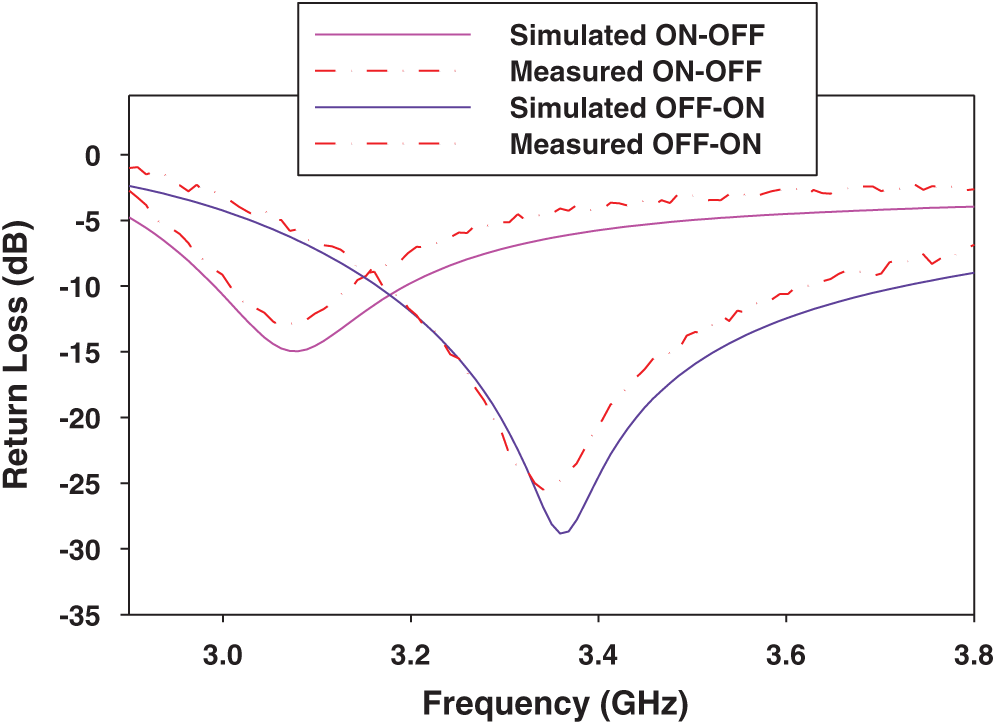
Figure 12: Simulated and measured S11 (in dB) of the proposed design
Fig. 13 give detail of the axial ratio bandwidth (ARBW) for both the switching arrangements. For ON-OFF state, the ARBW is 0.38 GHz (2.97–3.35 GHz) which is 42% of overall bandwidth and with 100% overlapping bandwidth. In OFF-ON state, the ARBW is 0.42 GHz (3.15–3.57 GHz). The CP performance for this switching arrangement is 76.36%. The simulated and measured ARBW are in close agreement for both the switching arrangements.
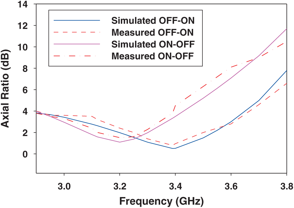
Figure 13: Simulated and measured axial ratio (in dB) of the proposed design
Fig. 14 shows the normalized simulated and measured radiation pattern for both the ON-OFF and OFF-ON states. These results were taken in Anechoic Chamber in University of Lorraine. Figs. 14a and 14b shows the E-field radiation pattern in XY plane and H-field in YZ plane for ON-OFF state. Similarly, Figs. 14c and 14d represents the E-field and H-field radiation pattern for OFF-ON state. The radiation patterns are measured at 3.1 and 3.37 GHz respectively. The radiation pattern for both the switching arrangements are stable and broadside with the good value of the gain. Measured radiation pattern also closely follow the simulated radiation pattern.
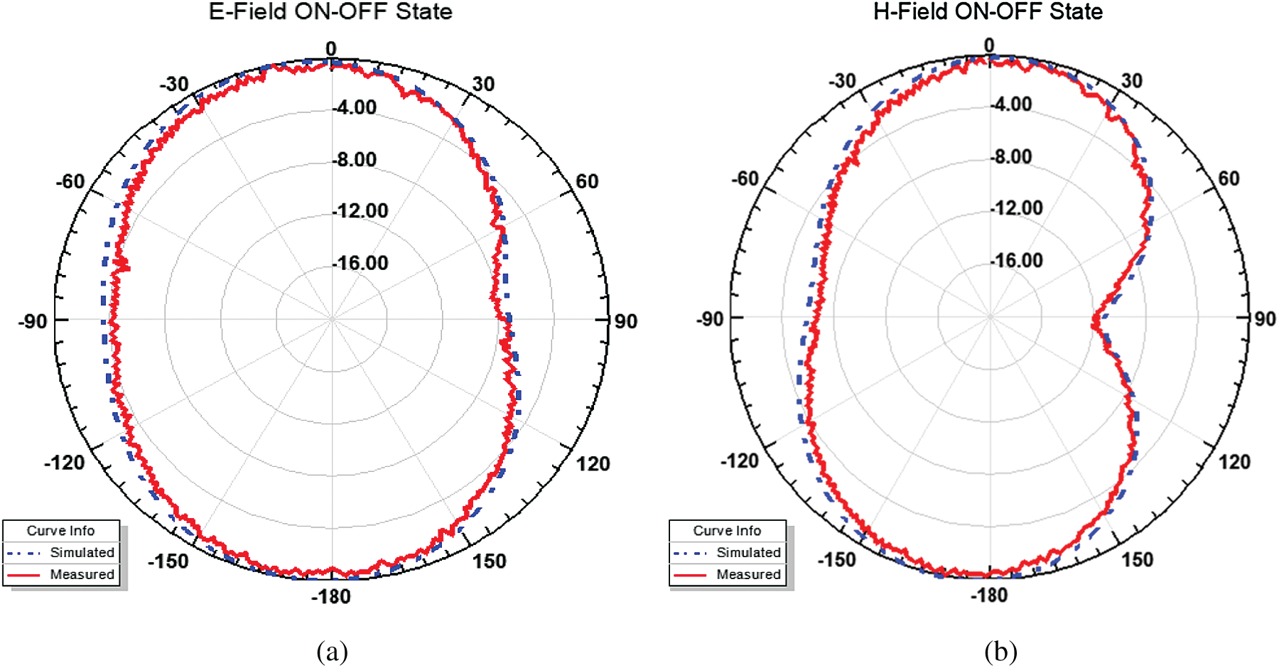
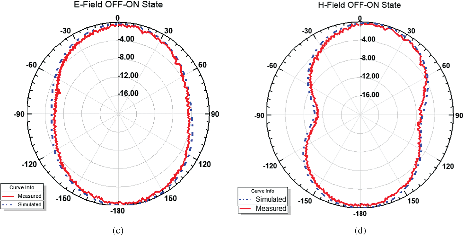
Figure 14: Simulated and measured radiation patter with (a) E-field (xy-plane) and (b) H-field (yz-plan) at 3.1 GHz and (c) E-field (xy-plane) and (d) H-field (yz-plane) at 3.37 GHz
Fig. 15 shows the simulated and measured peak gain for both the switching arrangements. The simulated peak gain for ON-OFF state is 3.4 dBi while due to fabrication intolerances the measured gain is slightly less than simulated value. Similarly, the measured peak gain for OFF-ON state at 3.37 GHz is 3.1 dBi. Both the simulated and measured gain are in close agreement. Overall performance of the proposed design is given in Tab. 2 in detail.
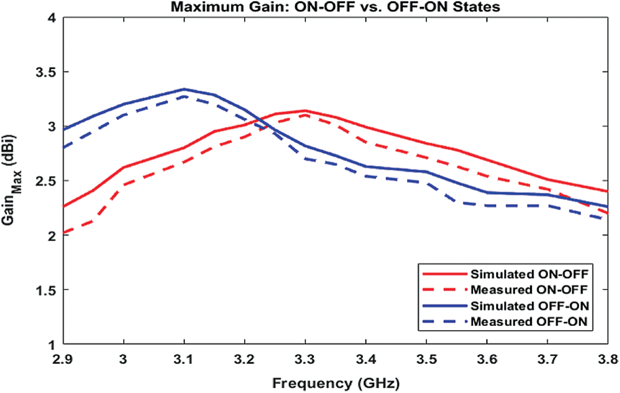
Figure 15: Simulated and measured peak gain for both the switching states
The performance analysis of the design is presented in Tab. 2. The simulated gain, radiation efficiency, ARBW and bandwidth have close resemblance with the measured values. There is slight degradation in measured bandwidth for ON-OFF state but the remaining parameters closely follow the simulated values which confirm the accuracy of the design. Figs. 16a–16c shows the fabricated design top and bottom view.
Table 2: Performance analysis table of the proposed design
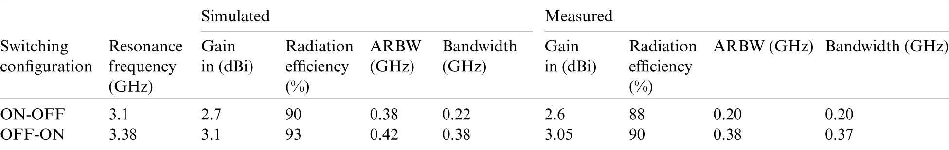
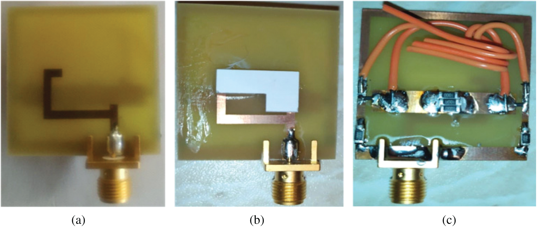
Figure 16: Fabricated prototype (a) extended feed-line without DR, (b) front view of the design, (c) bottom view of the design
Tab. 3 provides a detail comparison between the proposed work and some similar recent state of the art published work. The comparison is mainly based on some important parameters which include, the DR volume specifically height of the DR, operating bandwidth, achieved ARBW, overlapping ARBW and operating BW and availability of the reconfigurability features. From the Tab. 2 it is evident that the proposed design is the most compact with only 2 mm height.
Table 3: Comparison of the proposed design with the existing models
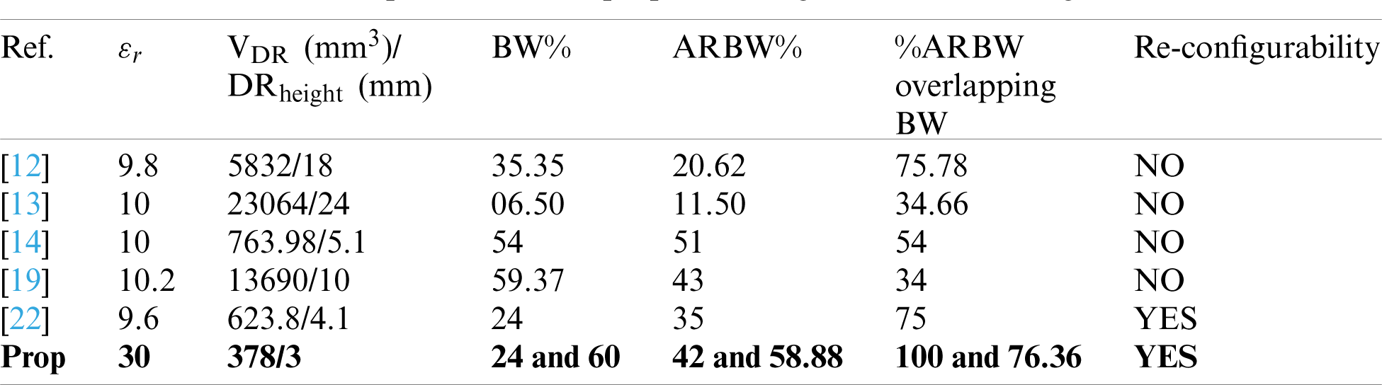
Additionally, the overall volume of the proposed design is very compact as compared to the other designs in the table. Moreover, because of the reconfigurability features, it offers two reconfigurable wide operating bandwidths with their corresponding wide axial ratio bandwidth. Due to lack of reconfigurability features, the other design in the table has no potential to reconfigure the different parameters of the designs. Additionally, the overlapping bandwidths for both the switching configurations are very good as compare to other examples. Thus, compact size, maximum overlapping bandwidth and reconfigurability features makes the design novel and useful).
A compact reconfigurable wideband circularly polarised DRA is presented. The reconfigurable CP DRA is fabricated and different performance parameters are measured. The CP mode is generated by extending the feed-line in the inverted question mark shape. A thin parasitic micro-strip line is positioned on the defective ground structure, which helps in achieving the required impedance bandwidth and axial ratio bandwidth. Two RF PIN Diodes switches connect this parasitic micro-strip line to the left and right side ground with the help of two switching arrangements. Configuration I offers 100% CP performance across 24% operating bandwidth with 40% ARBW while Configuration II offers 60% of the operating bandwidth and 58.88% ARBW with 73.36% CP performance. The proposed design is compact with 2 mm height (thickness) and 378 mm3 overall DR volume. Measured results show that proposed design is a good candidate for the target wireless applications.
Funding Statement: This work was supported by the National Science Foundation of China Grant funded by the Chinese Government (No. 61861043).
Conflicts of Interest: The authors declare that they have no conflicts of interest to report regarding the present study.
1. R. K. Mongia and P. Bhartia, “Dielectric resonator antennas—A review and general design relations for resonant frequency and bandwidth,” International Journal of Microwave and Millimeter-Wave Computer-Aided Engineering, vol. 4, no. 3, pp. 230–247, 1994. [Google Scholar]
2. A. Petosa and A. Ittipiboon, “Dielectric resonator antennas: A historical review and the current state of the art,” IEEE Antennas and Propagation Magazine, vol. 52, no. 5, pp. 91–116, 2010. [Google Scholar]
3. N. A. Jan, S. H. Kiani, F. Muhammad, D. A. Sehrai, A. Iqbal et al., “V-shaped monopole antenna with chichena itzia inspired defected ground structure for UWB applications,” Computers, Materials & Continua, vol. 65, no. 1, pp. 19–32, 2020. [Google Scholar]
4. D. A. Sehrai, F. Muhammad, S. H. Kiani, Z. H. Abbas, M. Tufail et al., “Gain-enhanced metamaterial based antenna for 5G communication standards,” Computers, Materials & Continua, vol. 64, no. 3, pp. 1587–1599, 2020. [Google Scholar]
5. O. M. Haraz, A. Elboushi, S. A. Alshebeili and A. R. Sebak, “Dense dielectric patch array antenna with improved radiation characteristics using EBG ground structure and dielectric superstrate for future 5G cellular networks,” IEEE Access, vol. 2, pp. 909–913, 2014. [Google Scholar]
6. S. Khan, H. Ali, R. Khan, R. Harry and C. Tanougast, “A cross-shaped MIMO reconfigurable dielectric resonator antenna for GSM and LTE/UMTS applications,” in 29th Irish Signals and Systems Conf., Belfast, pp. 1–4, 2018. [Google Scholar]
7. X. S. Fang. and K. W. Leung, “Linear-/circular-polarization designs of dual-/wide-band cylindrical dielectric resonator antennas,” IEEE Transactions on Antennas and Propagation, vol. 60, no. 6, pp. 2662–2671, 2012. [Google Scholar]
8. G. Massie, M. Caillet, M. Clenet and Y. M. M. Antar, “A new wideband circularly polarized hybrid dielectric resonator antenna,” IEEE Antennas and Wireless Propagation Letters, vol. 9, pp. 347–350, 2010. [Google Scholar]
9. R. Chair, S. L. S. Yang, A. A. Kishk, L. K. Fong and L. Kwai Man, “Aperture fed wideband circularly polarized rectangular stair shaped dielectric resonator antenna,” IEEE Transactions on Antennas and Propagation, vol. 54, no. 4, pp. 1350–1352, 2006. [Google Scholar]
10. Y. Pan and K. W. Leung, “Wideband circularly polarized trapezoidal dielectric resonator antenna,” IEEE Antennas and Wireless Propagation Letters, vol. 9, pp. 588–591, 2010. [Google Scholar]
11. K. Khoo, Y. Guo and L. C. Ong, “Wideband circularly polarized dielectric resonator antenna,” IEEE Transactions on Antennas and Propagation, vol. 55, no. 7, pp. 1929–1932, 2007. [Google Scholar]
12. R. Kumar and R. K. Chaudhary, “A wideband circularly polarized cubic dielectric resonator antenna excited with modified microstrip feed,” IEEE Antennas and Wireless Propagation Letters, vol. 15, pp. 1285–1288, 2016. [Google Scholar]
13. M. Khalily, M. R. Kamarudin, M. Mokayef and H. M. Jamaluddin, “Omnidirectional circularly polarized dielectric resonator antenna for 5.2-GHz WLAN applications,” IEEE Antennas and Wireless Propagation Letters, vol. 13, pp. 443–446, 2014. [Google Scholar]
14. A. Altaf and M. Seo, “An electronically-switched frequency-agile hybrid dielectric resonator antenna with a fixed reconfigurable circularly polarized band,” IEEE Access, vol. 8, pp. 143509–143518, 2020. [Google Scholar]
15. A. Altaf, J. Jung, Y. Yang, K. Lee and K. C. Hwang, “Reconfigurable dual-/triple-band circularly polarized dielectric resonator antenna,” IEEE Antennas and Wireless Propagation Letters, vol. 19, no. 3, pp. 443–447, 2020. [Google Scholar]
16. Y. Li and K. M. Luk, “Wideband perforated dense dielectric patch antenna array for millimeter-wave applications,” IEEE Transactions on Antennas and Propagation, vol. 63, no. 8, pp. 3780–3786, 2015. [Google Scholar]
17. J. Huang, “A technique for an array to generate circular polarization with linearly polarized elements,” IEEE Transactions on Antennas and Propagation, vol. 34, no. 9, pp. 1113–1124, 1986. [Google Scholar]
18. H. W. Lai, K. M. Luk and K. W. Leung, “Dense dielectric patch antenna—A new kind of low-profile antenna element for wireless communications,” IEEE Transactions on Antennas and Propagation, vol. 61, no. 8, pp. 4239–4245, 2013. [Google Scholar]
19. M. Khalily, M. R. Kamarudin and M. H. Jamaluddin, “A novel square dielectric resonator antenna with two unequal inclined slits for wideband circular polarization,” IEEE Antennas and Wireless Propagation Letters, vol. 12, pp. 1256–1259, 2013. [Google Scholar]
20. M. Khalily, M. K. A. Rahim and A. A. Kishk, “Planar wideband circularly polarized antenna design with rectangular ring dielectric resonator and parasitic printed loops,” IEEE Antennas and Wireless Propagation Letters, vol. 11, pp. 905–908, 2012. [Google Scholar]
21. R. Khan, J. U. R. Kazim, A. A. Khan, S. Aqeel, Owais et al., “A reconfigurable dielectric resonator antenna with pattern diversity for DVB-H application,” in Int. Conf. on Intelligent Systems Engineering, Islamabad, pp. 222–225, 2016. [Google Scholar]
22. W. Sun, W. Yang, L. Guo, W. Qin and J. Chen, “A circularly polarized dielectric resonator antenna and its reconfigurable design,” IEEE Antennas and Wireless Propagation Letters, vol. 19, no. 7, pp. 1088–1092, 2020. [Google Scholar]
 | This work is licensed under a Creative Commons Attribution 4.0 International License, which permits unrestricted use, distribution, and reproduction in any medium, provided the original work is properly cited. |