DOI:10.32604/cmc.2021.015759
| Computers, Materials & Continua DOI:10.32604/cmc.2021.015759 | |
| Article |
A Novel Design of Octal-Valued Logic Full Adder Using Light Color State Model
Department of Computer Science, Faculty of Computes and Information, Mansoura University, Mansoura, 35516, Egypt
*Corresponding Author: Osama Abu-Elnasr. Email: mr_abuelnasr@mans.edu.eg
Received: 05 December 2020; Accepted: 06 January 2021
Abstract: Due to the demand of high computational speed for processing big data that requires complex data manipulations in a timely manner, the need for extending classical logic to construct new multi-valued optical models becomes a challenging and promising research area. This paper establishes a novel octal-valued logic design model with new optical gates construction based on the hypothesis of Light Color State Model to provide an efficient solution to the limitations of computational processing inherent in the electronics computing. We provide new mathematical definitions for both of the binary OR function and the PLUS operation in multi valued logic that is used as the basis of novel construction for the optical full adder model. Four case studies were used to assure the validity of the proposed adder. These cases proved that the proposed optical 8-valued logic models provide significantly more information to be packed within a single bit and therefore the abilities of data representation and processing is increased.
Keywords: Mathematical modeling; numerical simulations; optical logic; optics in computing; multi-valued logic; full adder
Arithmetic operation plays an important role in various digital systems such as computers process controller and signal processors. Nowadays, computer depends on 2-ary conventional system with 2 logical states ‘Low’ and ‘High’. Binary Logic (BL) is a classical two-valued Boolean logic that development in it be founded difficult to understand and complex.
Because the demand for high speed computational operations for solving complex problems and high bandwidth has rapidly increased to get the maximum device speed, the future of computation and communication face problems of unavoidability. This is because the conventional electronic technology will very soon reach its speed limit. So, researchers are looking at several approaches to find alternatives to address these problems. One of these approaches is the optical signal processing that refers to a wide range of optical data signals techniques [1]. It includes vastly popular systems such as optical multiplexing and demultiplexing, equalizers, optical switches, optical memories, optical amplifiers [2,3], and various areas of microwave photonics [4,5].
Another parallel alternative is Multi-Valued Logic (MVL) that can enable significantly more information to be packed within a single digit instead of BL. It is considered another way of solving many complications of transmitting, saving, and dealing with large amount of information in digital signal processing [6].
Unlike BL that contains only ‘T’ and ‘F’ states, MVL has a root greater than 2 and contains values with a finite and unlimited number of values [7]. Recently, MVL is used for high-speed arithmetic operations due to its high speed and carries less generation. A carry free arithmetic operation can be achieved using MVL. Since a huge number of gates are presented in MVL, circuit complexity will be less and require small area than binary computer [8].
Recently, Optical Multi-Valued Logic (OMVL) functions have been shown a great importance in the last years towards optical logic and information processing applications. Applying OMVL can overcome the limitations faced by traditional binary electronic technologies. This technology could be a revolution in achieving very high levels speed of data processing. Also, it provides a complexity inherent in electronics computing system [9].
Most of the existed MVL models are depending on Three-Valued Logic (3-VL) [10–18] and Four-Valued Logic (4-VL) [19,20]. They follow the mechanism of the polarization encoded optical shadow casting scheme help which vertical and horizontal strips of opaque and transparent bars represent the logical states.
We aim in this work to define a new mathematical model based on OMVL that can execute the basic computational operations for enhancing the speed of processing data and the amount of processed information. Mainly, this paper proposes new optical logic gates and reshape how to extend them to define the optical model of the PLUS operation which can derive the other operations from. It is organized as following. Section 1 presents the literature review and related works. Section 3 discusses the proposed optical binary OR gate. Section 4 presents the mathematical model of defining the PLUS operation. Section 5 provides an explanation of the construction of an optical full adder as an application of the defined mathematical model with validating it. Finally, we provide the conclusions of the work.
Most of the efforts focus on extending classic binary logic to multi-valued logic to increase their abilities in representation and data processing. These efforts concentrate on implementing MVL in the fields of electronics using Metal-Oxide Semiconductor (MOS), Carbon Nanotube Field Effect Transistors (CNFET), and Quantum-dot Cellular Automata (QCA) technologies. Also, MVL is implemented in optical field using either many technologies that will listed in this section.
MOS is one of the earlier strategies used to design ternary logic circuit. Balla et al. [10] pro-posed an MOS ternary-logic family which includes a set of inverters, NAND gates, and NOR gates that were used to design basic 3-VL arithmetic and memory circuits. The circuits thus developed are shown to have low power dissipation, and reduced propagation delay and component count compared to other known ternary circuits.
Carbon Nanotube Field Effect Transistors (CNFET) provided an alternative technique to MOS transistors in the application areas that require high performance computations and low power consumptions. Merlin et al. [14] had been utilized CNFET and introduced a strategy that enabled carry Propagate-Generate to be used in a ternary addition leading to the use of 3-VL prefix adders. Also, their results showed that the delay was reduced (up to 28%) by using binary prefix networks for calculating the carry and obtain lower power (up to 29%) by using low power encoder.
Bhoi et al. [11] proposed a redundant adder architecture using QCA technology to improve the computation speed in ternary logic-based adders. Various experimentations were conducted and proved that Ternary QCA approach assures the efficiency of the proposed computational components; adder, decoder, and binary increment and decrement.
Li et al. [13] presented the design criteria of ternary MVL optical calculators based on Decrease-Radix Design rule. The experimentations which applied on hundreds-bit reconfigurable calculator state that the formation of any logic calculator can be constructed using a few basic units and hence increase the simplicity of the structures.
Datta et al. [21] presented an optical Full Adder design using switching mechanism of Mach–Zehnder Interferometers (MZI) based on Electro-Optic effect. It accepts three digital electrical signals and produces both sum and carry bits in optical domain. The simulations were carried out to validate the ability to handle power dissipation issue by passing three input control signals to the electrodes of three distinct groups of MZIs.
Roy et al. [16] proposed 3-VL half adder circuit with Optical Nonlinear Material switch (OPNLM) schema based on manipulating polarized lights of logical states. Various ternary optical circuits were constructed on the basis of the proposed half adder including; incrementer/ decrementer (INC/DEC) component and full adder circuit. Significant advantages were provided compared to some other circuits including: reduce the time lagging in data processing, minimize the required circuit components, and increase the computational performance.
Obiniyi et al. [15] suggested a design of Ternary Arithmetic and Logic Unit based on ternary color-coded for manipulating ternary calculations. Hence, they suggested modelling a ternary half adder circuit and separate carry value.
Patel et al. [22] presented arithmetic operations using MVL in both Modulo-4 arithmetic and Galois field. Also, Quaternary-binary and binary-quaternary converters, Negation in modular arithmetic, and quaternary multiplier circuit were proposed.
This paper establishes a novel MVL model with octal optical gates based on the different eight light colors to provide an efficient solution to the limitations of computational speed and complexity inherent in the electronics computing. Section 2.1 introduces hypothesis of modelling colors as logic states. Section 2.2 presents a new construction of optical binary OR gate, Optical Binary AND, Optical NOT, and optical dispersion gate from the standpoint of physics laws.
3.1 Hypothesis of Light Color State Model (LCSM)
Nowadays, most of computers and some types of printers use (Red–Green–Blue) RGB or (Cyan–Magenta–Yellow–Black) CMYK coloring systems to generate colored images and photos. In this research, we present the RGB and CMYK coloring systems not for generating images but to prove that they can be used in constructing the basis of the color numbering model that enhances the computational operations due to their abilities to generate thousands of various visible colors by changing the grey levels of basic colors processes.
Logic Color State Model (LCSM) is a numerical representation model in which a color represents an octal logic sate. Fig. 1 shows RGB light coloring model. Suppose that the red and green light colors are represented by  and
and  , respectively. According to the optical observations by projecting R and G together on a surface, it gives the wave intensity of yellow light color which can be stated as
  .
.
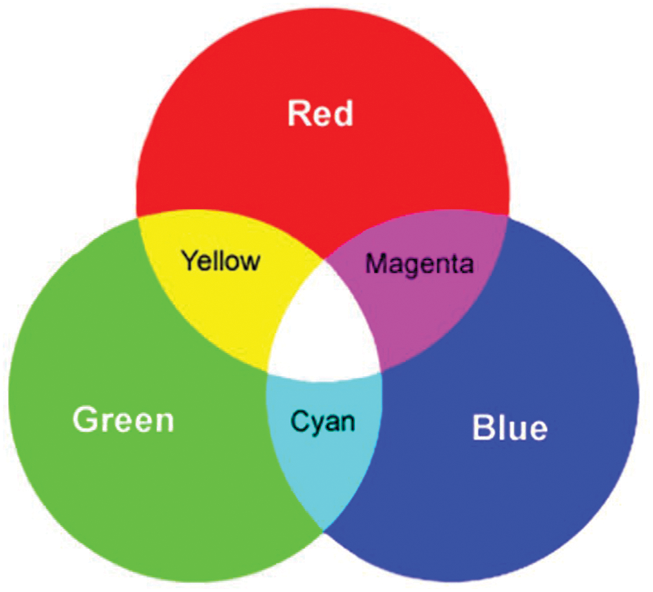
Figure 1: RGB light coloring model
In the same sense, if the blue light color is represented by  , then by projecting R with B, it gives magenta light color which can be stated as
  . Also projecting G with B gives cyan light color which can be stated as
  . The white light color consists of the three basic colors Red (R), Green (G), and Blue (B), and it can be stated as
  . By considering the black color as an infrared that can be added to any light color, it is represented by
  in our color light sate model. Fig. 2 shows the color logic states by representing each color with its value. Tab. 1 illustrates the mapping between each logic color state and its corresponding basis numbers within our proposed 8-VL.
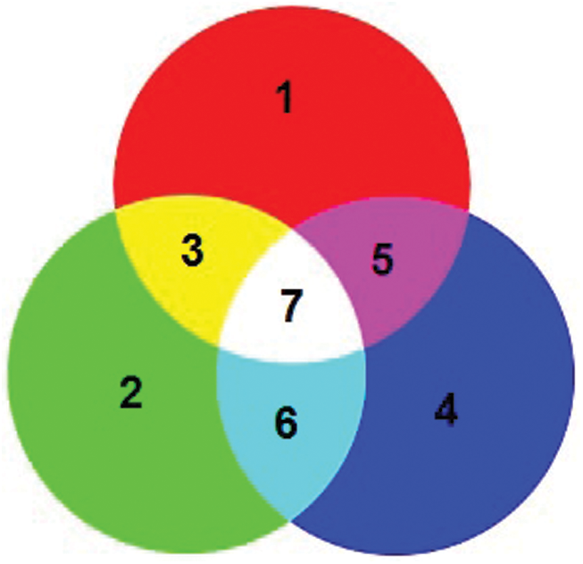
Figure 2: Light color state model
Table 1: Mapping of logic color states to its corresponding basis numbers

3.2 Basic Functions and Optical Gates
Like binary logic, many basic functions are existed in MVL. They are differing based on the base and number of used variables. Different logic functions could be constructed depending on MVL. The proposed MVL 8-VL is consists of 8 logical states K, R, Y, G, B, M, C, W. Set  and
and  , a function
  , then the number of possible functions
  that can be generated is calculated according to Eq. (1), [7]:

Where N is the number of possible functions, b is the base or radix, and n is the number of variables used in the function. In binary logic of one variable (b = 2, n = 1), there are 4 possible functions. When b = 2, n = 2, then f(2, 2) = 2(2)2 = 8. The possible functions of one input variable for 8-VL is f(8, 1) = 8(8)1 = 16,777,216, and their numbers for two variables  . These numbers are very huge. Hence, incredible numbers of functions or logical gates can possible for more variables. The next subsections discuss in detail the basic functions associated with our proposed 8-VL including: optical binary OR, Optical Binary AND, Optical NOT, and optical dispersion gates.
The behavior of the proposed optical binary OR gate simulates the behavior of the additive light property. In fact, they both obtain one optical beam in response to projection of more than one optical beam onto special types of prism or optical fibers to be one beam as shown in Fig. 3.
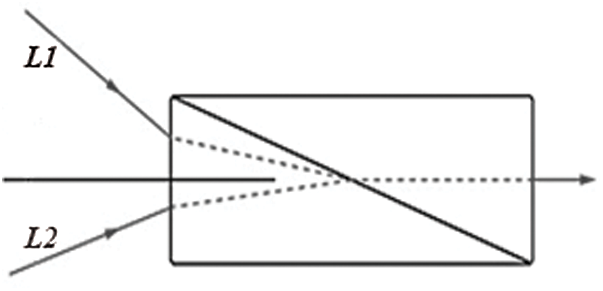
Figure 3: Additive light property
Let  , and X = (l1, l2), where
  , an optical binary OR function
  can be modelled as:
  . Where (
 ) means a binary OR operation by applying the or truth table on the binary representation of inputs, The symbolic representation of the optical binary OR gate of input X and Y is shown in Fig. 4. Tab. 2 illustrates the truth table of the possible states in the proposed 8-VL emergent from mixing two color lights A and B. It is denoted by
  and gets 64 resultant values.
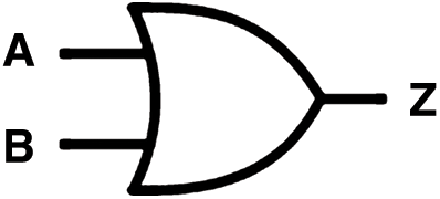
Figure 4: A Symbolic representation of optical binary OR gate
Table 2: Truth table of optical binary OR gate, 

The idea of the construction of light filters is to selectively transmit the desired wavelengths while restricting others. The two most common used types of filters are absorption and interference filters. Our proposed optical binary AND gate mimics the behavior of the absorption filters that absorb unwanted wavelengths, while the proposed optical binary NOT gate mimics the behavior of the interference filters in the way of removing selected wavelengths by internal destructive interference and reflection. Fig. 5 shows the mechanism of implementing a magenta filter that selectively transmits the red and blue portions of the incident white light spectrum and absorbs most of the green wavelengths.

Figure 5: Magenta absorption filter
Optical Binary AND Red Gate. Optical binary AND Red gate is built based on the work behavior of the red absorption filter. It is denoted by  that accepts optical light X and performs binary AND operation with red light.
Let  , and X = (l) where
  , then
  can be modeled as function
  ,where
  . Where (&) means binary AND operation by applying And truth table on the binary representation of inputs. Fig. 6 shows the symbolic representation of the optical binary AND Red gate of
  and Tab. 3 illustrates its truth table.

Figure 6: Symbolic representation of optical binary AND Red gate
Table 3: Truth table of optical binary AND Red gate, 

Another Binary AND Gates. The absorption filters can be applied to any sort of color state to design other optical AND gates. Let  , X = (l), and l,
  then
then  can be modelled as function
  , where
  .
.  ,
,  ,
,  ,
,  and
and  are optical Binary AND gates that accept one optical light X and perform binary AND operation with the specified built-in color light. Fig. 7 shows their symbolic representations while Tab. 4 illustrates their truth tables.

Figure 7: The symbolic representation of other optical AND gates
Table 4: Truth table of other optical binary AND gates,  ,
,  ,
,  ,
,  and
and 

Our proposed negation gate (i.e., optical binary NOT gate) is constructed based on the work behavior of the interference filters. Unlike the absorption filters, the interference filters reflect and destructively interfere with unwanted wavelengths as opposed to absorbing them. The term dichroic arises from the fact that the interference filter appears one color under illumination with transmitted light and another color with reflected light. Fig. 8 shows how the magenta dichroic filter reflects the green light and permitting the magenta light to be transmitted from the other side of the filter.

Figure 8: Magenta interference filter
Optical NOT Red Gate. Optical binary NOT Red gate is built based on the work behavior of the cyan interference filter. The cyan dichroic filter reflects the red light and permitting the cyan light to be transmitted from the other side of the filter. The reflected light performs  operation and is denoted by
  . Let
. Let  , and X = (l),
  , then optical binary NOT Red gate (
 ) can be modelled as function
  , where
  . Fig. 9 shows the symbolic representation of the optical binary NOT Red Gate of
  and Tab. 5 illustrates its truth table.

Figure 9: The symbolic representation of optical Not Red gate
Table 5: Truth table of optical NOT Red gate, 

Another Optical Binary NOT Gates. As we worked through designing the optical binary NOT Red gate by implementing the behavior of the cyan interference filter, the other colored filters can be used to design with related color the other optical NOT gates.
Let  , X = (l), and
  then
then  can be modelled as function
  , where
  .
.  ,
,  ,
,  ,
,  and
and  are optical Binary NOT gates that accept optical light X and perform negation operation of the specified built-in color light. Fig. 10 shows their symbolic representations and Tab. 6 illustrates their truth tables.

Figure 10: The symbolic representation of other optical NOT gates
Table 6: The truth table of other optical binary NOT gates,  ,
,  ,
,  ,
,  and
and 

The behavior of our proposed optical dispersion gate simulates the behavior of the dispersion light property. In fact, they both accept one optical beam and disperse the projected light to its basic constituent colors as shown below in Fig. 11.

Figure 11: Dispersion light property
So far, there are two types of the optical dispersion gate based on their ability to disperse lights. The first one can disperse the projected light color to its all constituent logical states as shown in Fig. 11. The other type is one that disperses the input projected light color to its three basic constituent logical states as called shown in Fig. 12. Our proposed optical 3-Dispersion Gate (3DG) follows the characteristics of the second type. Fig. 13 shows the symbolic representation of the optical dispersion gate and Tab. 7 illustrates its truth table.
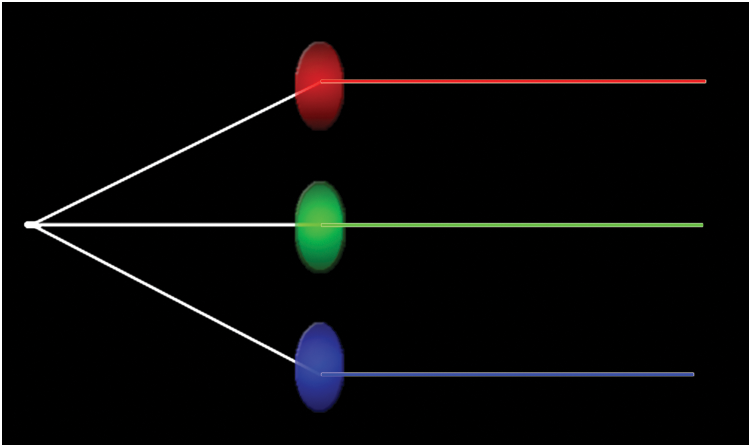
Figure 12: Optical 3-dispersion filters

Figure 13: Symbolic representation of optical 3-dispersion gate
Table 7: Truth table of optical 3-dispersion gate

4 Proposed Mathematical Model of PLUS Operation in MVL
The proposed model provides a new definition for the PLUS operation based on the definition of binary OR gate in MVL. Section 4.1 defines the binary OR function. Section 4.2 defines the PLUS operation for any MVL. Section 4.3 highlights the definition of the plus-carry function.
4.1 Mathematical Definition of Binary OR Function
Binary OR function defined in binary logic as:  is True when A OR B, or both, are True but in MVL has another definition. Let
  is the set of powers of 2 where
  , if we have Zn is MVL with n states where
  , and
, and  then
then  are the set of powers of 2 that found in a, b respectively, these sets A, B calculated according to Eq. (2).

Where i is the position of the index of element of 2’s power in set A. The Binary OR function in MVL  is calculated by modulo n of summation of not repeated powers of 2 that found in inputs a and b in other words
  calculated by Eq. (3).

For example: Suppose we have  and let a = 3, b = 1 and the sets of powers of 2 for a, b
  ,
,  then
then  and
and  .
.
The binary OR function of  can work as PLUS function on Zn of a, b if there is no repeated powers of 2 appear in input sets A, B and that means
  if
if  . So, binary OR function will not equal PLUS function in cases that powers of 2 is repeated in the set A, B; in other words:
  if
if  , Ai = Bj. for example: Suppose we have
  as MVL and let a = 3, b = 1 and
  ,
,  then
then  where
where  and (a + b)Zn = 0 so,
  .
.
4.2 Mathematical Definition of PLUS Operation
Form binary OR operation definition, we can add a new definition of PLUS operation for any MVL as binary OR operation with replacing the cases that has repeated Powers of 2 of inputs with another value  that matched with PLUS operation, by define
  ,
,  ,
,  ,
,  ,
,  where n is the number of states in MVL. This
  value will be a new input to the recursive PLUS function with
  , until there is no any repeated item then applying binary or operation, the final
  definition of can defined by Eq. (4).

The definition of  Value is changed from MVL to another. In our case of 8-VL,
  have the values:
  ,
,  ,
,  .
.
For example: Suppose  as MVL , let a = 3, b = 1 and
  ,
,  , and
, and  value in Z4 defined as 1+1 = 2, 2+2 = 0. Thus:
  and
and  . Here,
  by setting
  and applying the Eq. (4) then
  by applying the recursive Eq. (4) again on the result by replacing
  then
then  and
and  then
then  then
then  will be 0.
4.3 Mathematical Definition of Plus-Carry Function
The carry value C of PLUS operation is the next state of the result if the summation greater than or equals the number of states in MVL. For any MVL Zn for a, b  Zn can also depend on the sets of powers of 2
  that found in a, b. The C value will be the first state of Zn if there exist a summation of two or more powers of 2 is greater than n so C can be calculated according to Eq. (5)

For example: In binary logic, the only state that gives carry value is: (1+1), in 3-VL (1+2, 2+2), in 4-VL there is one case (2+2) and so on. In our case study 8-VL, there is only one case can give carry value if exist (4+4) in the set of powers of 2 in PLUS operation.
5 Architecture of Optical Full Adder (OFA)
The full adder in the binary logic circuits represents the main core of any micro-controller or processor. The subsequent sub-sections implement the defined mathematical model of PLUS operation by representing an optical full adder construction based on proposed optical 8-VL gates. Section 5.1 uncovers the principle and the implementation of constructing the optical tiny adders. Section 5.2 discusses in detail the design of the proposed optical full adder. Section 5.3 introduces set of case studies to validate the functionality of the optical full adder.
The architecture of the proposed optical adder is consisting of three tiny adders: Optical Red Tiny Adder (ORTA), Optical Green Tiny Adder (OGTA), and Optical Blue Tiny Adder (OBTA). The idea behind constructing the tiny adders is built on extending the abilities of manufactured nonlinear materials that can double the frequency of the light passes through them and generates new light [23]. Each tiny adder may be constructed using one optical component or sort of simple optical gate.
5.1.1 Optical Red Tiny Adder (ORTA)
ORTA is one type of OTA that can only makes PLUS operation on 3 Red beams as input values and the output may be red or green or both. Let  , and L1,
  where
where  , and
, and  and l1, l2,
  , Then, ORTA can be modelled as the function
  where f defined as in Eq. (6). Fig. 14 shows the simple circuit design of ORTA given inputs; L1, L2 and
  and Tab. 8 illustrate its truth table.


Figure 14: ORTA circuit design
Table 8: Truth table of optical red tiny adder, ORTA

5.1.2 Optical Green Tiny Adder (OGTA)
OGTA is another type of OTA that can only make PLUS operation on 3 green beams as input values and the output may be either green or blue or both. Let  , and L1,
  where
where  , and
, and  and l1, l2,
  , Then OGTA can be modelled as the function
  where f defined as in Eq. (7). Fig. 15 shows the simple circuit design of OGTA given inputs; L1, L2 and
  where Tab. 9 illustrate its truth table.


Figure 15: OGTA circuit design
Table 9: Truth table of optical green tiny adder, OGTA

5.1.3 Optical Blue Tiny Adder (OBTA)
OBTA is another type of OTA that can only make PLUS operation on 3 blue beams as input values and the output may be blue or red or both. Let  , and L1,
  where
where  , and
, and  , and l1, l2,
  , Then, OBTA can be modelled as the function
  where f is defined as given in Eq. (8). Fig. 16 shows the simple circuit design of OBTA given inputs: L1, L2 and
  where Tab. 10 illustrates its truth table.


Figure 16: OBTA circuit design
Table 10: Truth table of optical blue tiny adder, OBTA

5.2 Optical Full Adder (OFA) Design
Optical Full Adder (OFA) is an optical device that implements the PLUS operation of two octal values. It consists of the three types of the tiny adders; ORTA, OGTA, and OBTA. OFA has three input values: L1, L2, and empty value of Cin and generate Z as a summation result of the PLUS operation and CO as the resultant carry. Tab. 11 illustrates the truth table of OFA.
Table 11: Truth table of optical full adder, OFA

The design of OFA is consisting of two optical 3-dispersion gates followed by three optical tiny adders; ORTA, OGTA, OBTA and then an optical binary OR gate as shown in Fig. 13. The projected light colors L1 and L2 are dispersed to their basic constituent colors using the first and the second optical 3-dispersion gates respectively. The dispersed lights are propagated to their related optical tiny adders. The resultant values of the three tiny adders are passed through the optical binary OR gate to produce Z as the result of the PLUS operations. The carry CO is emitted at the end from OBTA as a red value as illustrated above in Tab. 11. The resultant carry value is connected as a carry input to another OFA in the chain of computation as shown in Fig. 17.

Figure 17: OFA circuit design
5.3 Validation of the Proposed Models
In order to assure the validity of the defined mathematical model of the PLUS operation and hence the proposed optical full adder model, four case studies are used according to the description illustrated in Tab. 12.
Table 12: Input–Output mapping of case studies

In Case study (I), the inputs values are G and B as L1 and L2 inputs to optical 3-dispersion gates (3DG1) and (3DG2) respectively, the output of (3DG1) will be G, that will connected as first input of OGTA, and the output of (3DG2) will be B connected as a second input of OBTA, the output of OGTA is G, and the output of OBTA is B, the output values G and B will be inputs to binary OR Gate and the output will be C. In Case study IV, the inputs values are C and M as L1 and L2 inputs to (3DG1) and (3DG2) respectively the output of (3DG1) will be G and B that will connected as first inputs of OGTA and OBTA respectively, the output of (3DG2) will be R and B connected as a second inputs of ORTA and OBTA respectively, the output of ORTA is R and output of OGTA is G, the output of OBTA is R, the output values R and G will be inputs to the binary OR Gate and the output will be Y and the carry value is R. Tab. 13 display the inputs and outputs of each case for all components in OFA.
Table 13: Input–Output trace of the case study

In this paper, a new optical 8-VL model was proposed to provide an efficient approach for handling the computational speed and complexity issues in the classical logic. CLSM was defined as a numerical color representation model for describing the optical logical states. The proposed optical gates in 8-VL were constructed and their truth table were defined. The optical binary OR gate mimics the behavior of the additive light property. The optical binary AND gate mimics the behavior of the of the absorption filter. The optical binary NOT gate mimics the behavior of the of the interference filter. The optical dispersion gate mimics the behavior of the of the dispersion light property filter. We introduced a new definition for the binary OR function that led us to establish a new mathematical representation for the PLUS operation in MVL. Also, a novel construction for the full adder that sum octal numbers in optical MVL is proposed. Four case studies were used and proved the validity of the proposed models.
Funding Statement: The authors received no specific funding for this study.
Conflicts of Interest: The authors declare that they have no conflicts of interest to report regarding the present study.
1. A. E. Willner. (2013). “Optical signal processing,” in Optical Fiber Communication Conf., Anaheim, California, United States, p. OM2G.5: Optical Society of America. [Google Scholar]
2. M. T. Hill, H. J. Dorren, T. de Vries, X. J. Leijtens, H. J. den Besten et al. (2004). , “A fast low-power optical memory based on coupled micro-ring lasers,” Nature, vol. 432, no. 7014, pp. 206–209. [Google Scholar]
3. K. Nozaki, A. Shinya, S. Matsuo, Y. Suzaki, T. Segawa et al. (2012). , “Ultralow-power all-optical RAM based on nanocavities,” Nature Photonics, vol. 6, no. 4, pp. 248–252. [Google Scholar]
4. J. Capmany and D. Novak. (2007). “Microwave photonics combines two worlds,” Nature Photonics, vol. 1, no. 6, pp. 319–330. [Google Scholar]
5. J. Yao. (2009). “Microwave photonics,” Journal of Lightwave Technology, vol. 27, no. 3, pp. 314–335. [Google Scholar]
6. C. Porzi, M. Scaffardi, L. Potì and A. Bogoni. (2010). “Optical digital signal processing in a single SOA without assist probe light,” IEEE Journal of Selected Topics in Quantum Electronics, vol. 16, no. 5, pp. 1469–1475. [Google Scholar]
7. R. Cunha, H. Boudinov and L. Carro. (2007). “Quaternary look-up tables using voltage-mode CMOS logic design,” in 37th Int. Symp. on Multiple-Valued Logic, Oslo, Norway, IEEE, pp. 56. [Google Scholar]
8. T. Chattopadhyay and J. N. Roy. (2011). “All-optical multi-valued computing: The future challenges and opportunities,” in Int. Conf. on Convergence of Optics and Electronics, Kolkata, pp. 94–101. [Google Scholar]
9. D. Gayen, A. Bhattacharyya, R. Pal and J. N. Roy. (2011). “All-optical binary-coded decimal adder with a terahertz optical asymmetric demultiplexer,” Computing in Science & Engineering, vol. 13, no. 1, pp. 50–57. [Google Scholar]
10. P. C. Balla and A. Antoniou. (1984). “Low power dissipation MOS ternary logic family,” Journal of Solid-State Circuits, vol. 19, no. 5, pp. 739–749. [Google Scholar]
11. B. K. Bhoi, N. K. Misra, I. Dash and A. Patra. (2020). “A redundant adder architecture in ternary quantum-dot cellular automata,” in Smart Intelligent Computing and Applications, Berlin, Germany: Springer, pp. 375–384. [Google Scholar]
12. S. Kim, S. Y. Lee, S. Park, K. R. Kim and S. Kang. (2020). “A logic synthesis methodology for low-power ternary logic circuits,” IEEE Transactions on Circuits and Systems I: Regular Papers, vol. 67, no. 9, pp. 3138–3151. [Google Scholar]
13. C. Li and J. Yan. (2010). “Design method and implementation of ternary logic optical calculator,” in Int. Conf. on Computer and Computing Technologies in Agriculture, Berlin, Germany, Springer, pp. 147–166. [Google Scholar]
14. J. L. Merlin, T. A. Khan and T. S. Hameed. (2020). “Design of a low power three bit ternary prefix adder using CNTFET technology,” AIP Conf. Proc., vol. 2222, no. 1, pp. 20005. [Google Scholar]
15. A. A. Obiniyi, E. E. Absalom and K. Adako. (2011). “Arithmetic logic design with color-coded ternary for ternary computing,” International Journal of Computer Applications, vol. 26, no. 11, pp. 31–37. [Google Scholar]
16. J. N. Roy, P. Bhowmik and T. Chattopadhyay. (2015). “Design of all optical ternary logic based half adder circuit and it’s applications,” Journal of Optics, vol. 44, no. 4, pp. 322–329. [Google Scholar]
17. A. Stakhov. (2002). “Brousentsov’s ternary principle, Bergman’s number system and ternary mirror-symmetrical arithmetic,” Computer Journal, vol. 45, no. 2, pp. 221–236. [Google Scholar]
18. J. Yi, H. Huacan and L. Yangtian. (2005). “Ternary optical computer architecture,” Physica Scripta, vol. 2005, no. T118, pp. 98. [Google Scholar]
19. S. A. Hosseini and E. Roosta. (2020). “A novel low complexity and energy-efficient method to implement quaternary logic function in nanoelectronics,” Microelectronics Journal, vol. 102, no. 2, pp. 104821. [Google Scholar]
20. A. Raja, K. Mukherjee, J. Roy and K. Maji. (2020). “Analysis of new all-optical polarization-encoded quaternary Galois field adder processing soliton pulses,” Journal of Optics, vol. 49, no. 1, pp. 83–93. [Google Scholar]
21. S. Datta and S. Es. (2020). “Design of an optical full adder based on electro-optic effect in mach-zehnder interferometers,” in National Conf. on Emerging Trends on Sustainable Technology and Engineering Applications, Durgapur, Burdwan, India, IEEE, pp. 1–5. [Google Scholar]
22. V. Patel and K. Gurumurthy. (2010). “Arithmetic operations in multi-valued logic,” International Journal of VLSI Design & Communication Systems, vol. 1, no. 1, pp. 21–32. [Google Scholar]
23. M. Taghinejad, Z. Xu, K. T. Lee, T. Lian and W. Cai. (2020). “Transient second-order nonlinear media: Breaking the spatial symmetry in the time domain via hot-electron transfer,” Physical Review Letters, vol. 124, no. 1, pp. 13901. [Google Scholar]
 | This work is licensed under a Creative Commons Attribution 4.0 International License, which permits unrestricted use, distribution, and reproduction in any medium, provided the original work is properly cited. |