| Computer Modeling in Engineering & Sciences |
DOI: 10.32604/cmes.2022.018037
ARTICLE
Numerical and Experimental Investigations of the Thermal Fatigue Lifetime of CBGA Packages
1School of Reliability and Systems Engineering, Beihang University, Beijing, 100191, China
2Sichuan Institute of Solid-State Circuits, China Electronics Technology Group Corporation, Chongqing, 400060, China
3School of Mechanics, Civil Engineering and Architecture, Northwestern Polytechnical University, Xi’an, 710072, China
*Corresponding Authors: Bo Wan. Email: wanbo@buaa.edu.cn; Xu Long. Email: xulong@nwpu.edu.cn
Received: 24 June 2021; Accepted: 04 August 2021
Abstract: A thermal fatigue lifetime prediction model of ceramic ball grid array (CBGA) packages is proposed based on the Darveaux model. A finite element model of the CBGA packages is established, and the Anand model is used to describe the viscoplasticity of the CBGA solder. The average viscoplastic strain energy density increment ΔWave of the CBGA packages is obtained using a finite element simulation, and the influence of different structural parameters on the ΔWave is analyzed. A simplified analytical model of the ΔWave is established using the simulation data. The thermal fatigue lifetime of CBGA packages is obtained from a thermal cycling test. The Darveaux lifetime prediction model is modified based on the thermal fatigue lifetime obtained from the experiment and the corresponding ΔWave. A validation test is conducted to verify the accuracy of the thermal fatigue lifetime prediction model of the CBGA packages. This proposed model can be used in engineering to evaluate the lifetime of CBGA packages.
Keywords: CBGA packages; lifetime prediction; finite element method; thermal fatigue; Anand model; Darveaux model
As electronic products have become smaller, lighter, and more reliable, ceramic ball grid array (CBGA) packaging has been increasingly used in electronic products. As a critical component of a stand-alone machine or a system, the failure of the CBGA device will cause the system to malfunction, resulting in high risks to product engineering. Therefore, the lifetime prediction of CBGA packages is essential to the reliability research of electronic products.
CBGA devices are high-density interconnect devices. In CBGA assembly, the device and the printed circuit board (PCB) are connected by soldering to form a component. The solder joints are prone to multiple failure modes during the assembly and subsequent testing under complicated loadings [1]. The failure modes of solder joints include false soldering and solder joint deformation. Failure significantly affects the device’s quality and solder joint reliability. These problems are caused primarily by improper control of the temperature and time parameters during soldering. Pang et al. [2] studied the changes in the microstructure of BGA solder joints under thermal cycling conditions and found that thermal cycling increased the grain coarseness. An intermetallic compound was located between the tin-lead solder interface and the pad, decreasing the strength of the solder joint and causing it to fail. Solomon et al. [3] analyzed the fatigue behavior of 60Sn40Pb solder at different temperatures. The research results of Zhang et al. [4] showed that thermal fatigue decreased the reliability of electronic components. Therefore, this article focuses on the number of thermal fatigue life cycles of a CBGA in a thermal cyclic profile. Zuo et al. [5] used the Engelmaier model, a strain-range-based fatigue model, to study the fatigue life of defective solder joints. Wan et al. [6] proposed an improved reliability evaluation method based on PoF technique and maximum entropy (MaxEnt) principle. The results showed that the proposed MaxEnt distributions can generate more reliable reliability evaluation results compared with Weibull distributions. Su et al. [7] conducted fatigue reliability design for Metal Dual Inline Packages under random vibration using finite element analysis, physics of failure model and surface response method. Wang et al. [8] conducted experiments to investigate the thermal behavior, mechanical properties of composite solder alloys and shear fracture behavior of solder joints. The test results reflected that the hardness and modulus of composite solder alloys were enhanced after the addition of Ni-CNTs. Fu et al. [9] analyzed thermal distributions and stress-strain distributions of the SiP by finite element analysis (FEA) tools based on hardware information and lifecycle profile of SiP. With the utilization of PoF models, lifetime matrix of the SiP is obtained.
The Anand viscoplastic model is a common model to describe the constitutive relationships of solders, and the viscoplasticity of solder material in a thermal environment. It uses a single internal variable to describe the resistance of the internal state of the material to plastic flow. This model relates the deformation behavior of viscoplastic materials to the strain rate and temperature. Amagai et al. [10–12] used the Anand model and revised it to investigate the deformation of SnPb series, SnZn series, SnAg series, and SnAgCu series solders at different humidities and strain rates. Wu et al. [13] used the Anand viscoplastic constitutive model to simulate the nano-silver sintered die-attachment in devices under thermal cyclic conditions. The simulation results showed that the bonding layer of the nano-silver paste experienced plastic strain under these conditions, which was the leading cause of the chip connection failure. Similar with previous works with the framework of the unified creep-plasticity model [14,15], Long performed extensive experimental studies with a wide range of temperature and strain rate and parameterized the Anand constitutive model with excellent agreement with measured stress–strain curves [16].
Many scholars have researched the reliability and lifetime prediction methods of solder joints. Che et al. [17] performed a thermal cycle finite element analysis on a plastic BGA package with Sn-3.8Ag-0.7Cu lead-free solder joints. They predicted and compared the fatigue life of solder joints using different 2-D and 3-D finite element analysis models. Wang et al. [18] proposed an advantageous mechanics-based acceleration approach to estimate the thermal fatigue life of BGA solder joints. Li et al. [19] conducted a stress-strain analysis on the simulation results of SnAgCu solder under thermal shock to evaluate different loading conditions and performed crack growth correlation and life prediction. Jiang et al. [20] used an energy-based life prediction model for BGA solder balls under thermal cyclic conditions and verified the correctness of the model and parameters through accelerated life tests. Hu et al. [21] proposed a thermal fatigue life prediction model for BGA solder joints considering the effect of the load sequence. The model improved the usability and accessibility of test data and verified the new failure criterion through experiments and simulations. Lee et al. [22] studied the effect of the size of the plastic-encapsulated BGA device substrate on the failure under thermal cyclic conditions. The study found that the thermal fatigue life of the solder balls had an inverse relationship with the substrate size.
Energy-based lifetime prediction models are also often used. Akay et al. [23] proposed a life prediction model for the number of failure cycles of a device. This model was used to predict the lifetime of a wireframe BGA package. Another energy-based model that considered the effects of elasticity and creep was proposed by Liang et al. [24]. This model is appliable to BGA packages. Darveaux [25] proposed a life prediction model for BGA packages/chip-scale packages (CSP) that is currently widely used. Chen et al. [26] applied the Darveaux model to predict the life of solder balls of stacked die packages under thermal cyclic conditions. The prediction results were used to verify the accuracy of the proposed optimization method. Li et al. [27] also used the Darveaux model to obtain the strain energy distribution during crack initiation in the expansion area of a quad flat package (QFP) using finite element simulation. The results showed that the average strain energy density was similar in the crack initiation zone, but the average strain energy density was different in the crack propagation zone, resulting in similar crack initiation times but different crack growth rates. Marbut et al. [28] simulated mechanical stress caused by shear stress resulting from the thermal expansion of a flip-chip device under thermal cyclic conditions and modified the Darveaux model parameters for lifetime prediction. Sitta et al. [29] used the Anand model and finite element methods to model discrete low-voltage packages and applied the Darveaux model for lifetime prediction. Zhang et al. [30] established a 3D slice model to analyze the reliability of solder joints. The time- and temperature-related creep properties of 63Sn37Pb solder were determined under thermal cyclic conditions. They used the Darveaux model to predict the thermal fatigue life of solder joints and studied the effect of the package size. The research results showed that the larger the chip size, the greater the maximum stress at the boundary was. They also found that the thickness of the bottom plate significantly affected the thermal failure of the package’s structure. This study uses the Darveaux model for the lifetime prediction of CBGA packages because the model exhibits good performance for BGA life prediction.
Based on previous research, it can be noticed that the Darveaux model has a very effective application in the field of solder life prediction. Through the Darveaux model, the number of life cycles can be quickly obtained. However, the correlation coefficients of the Darveaux model vary greatly for different structural designs, structural parameters and material characteristics of the package. Therefore, for typical CBGA packages, modification of the Darveaux model is required.
A life prediction model of CBGA packages is established using a finite element model of a CBGA and the Anand constitutive model to characterize the viscoplasticity of the solder. The average viscoplastic strain energy increment ΔWave is obtained from the finite element simulation, and the influence of different structural parameters on ΔWave is analyzed. Multiple regression analysis is used to establish a simplified analytical model of ΔWave. A thermal cyclic test is conducted to modify the parameters of the Darveaux life prediction model. Experiments are conducted to determine the number of thermal fatigue life cycles of a typical CGBA. In addition, a validation test is carried out to verify the accuracy of the life prediction model of CBGA packages.
2 Theory and Model Formulation
2.1 Viscoplastic Constitutive Model
The Anand model [31] is a constitutive equation used to describe the rate-dependent deformation of metals at high temperatures. The Anand model is a unified viscoplastic constitutive model. It comprehensively considers the creep deformation and plastic deformation that occur simultaneously during soldering. The unified constitutive model describes the mechanical behavior of solder in a straightforward manner and uses test data to identify the model parameters.
The Anand model has two basic characteristics: (1) The model does not have a clear yield surface in the stress space; thus, there is no need to provide loading and unloading criteria during deformation. Plastic deformation can occur under all non-zero stress conditions. (2) The model uses the deformation resistance s as a single internal variable. s represents the average resistance of the material’s internal state to the macroscopic plastic flow.
The Anand constitutive model describes the relationship between the strain rate and temperature and the deformation behavior of viscoplastic materials, strain hardening, the historical effect of the strain rate, and the dynamic recovery of strain. Initially, the Anand model was primarily used to describe the thermal properties of high-strength aluminum and other structural metals. It is currently widely used to describe the viscoplastic behavior of solder.
In the Anand model, the deformation resistance is proportional to the equivalent stress:
where c is the material parameter, which is expressed as:
where εp is the inelastic strain rate. ξ is the stress multiplier. A is the constant. Q is the activation energy. T is the environmental temperature. R is the gas constant. m is the strain rate sensitivity index.
The flow equation of the viscoplastic Anand model adopts the hyperbolic creep law, which is described as:
The evolution equation for the internal variable s is:
where h(σ,s,T) is the hardening function, which is related to the dynamic strain hardening and recovery process of the material. The hardening function is given by:
where h0 and a are the strain-hardening parameters of the performance material. s* is the saturation value of s and is expressed as follows:
where s' is the coefficient of the deformation resistance saturation value. n is the strain rate sensitivity. By combining Eqs. (4)–(6), s can be obtained as follows:
Accordingly:
Eq. (8) is related to the material’s saturation stress, temperature, and strain rate. Under isothermal conditions and if s* > s, the following applies:
By integrating the above Eq. (9), the following expression of the stress can be obtained:
where σ0 = cs0, and s0 is the initial value of s.
The stress-strain relationship can be calculated using Eq. (10), and the strain energy can be obtained based on the calculated stress and strain. The viscoplastic strain energy density is defined as the summation of the product of the stress and inelastic strain increment vectors divided by the number of converged subsets. The viscoplastic strain energy can be written as:
where WE is the plastic energy, σ is the stress vector, Δ εpl is the plastic strain increment, and vi is the volume of the integration points. The average of the strain energy density can be written as:
where N is the total number of selected analysis elements. i is the element number. vi is the element volume with the element number i. Wi is the average viscoplastic strain energy density of the element with the element number i. The average viscoplastic strain energy density increment ΔWave is given by:
where n and n − 1 are the cycle numbers. ΔWave is used as the input for the subsequent models.
2.2 Energy-Based Darveaux Model
The Darveaux life prediction model [25] is based on energy. This model considers the plastic energy exerted on the device under cyclic load conditions. The plastic energy dissipation can be obtained from the stress-strain hysteresis curve. The area of the curve represents the cumulative fatigue damage of the solder joints during thermal cycling.
The Darveaux life prediction model divides the crack propagation into two parts. In the first part, the model predicts the number of cycles during which cracks are initiated. The predicted number of cycles in this part is given by:
where N0 is the number of cycles during initial crack propagation. k1 and k2 are the correlation coefficients related to the solder joint material, the selected model, the thickness of the analysis unit, the grid division, and other parameters.
In the second part, the model uses fracture mechanics to predict the growth rate of the crack and deduce the number of cycles required for the crack to expand and lead to the complete failure of the area. The predicted number of cycles in this part is given by:
where k3 and k4 are the same correlation coefficients as k1 and k2. a is the characteristic fracture length, da/dN is the crack growth rate.
Finally, the two parts are combined to obtain the number of cycles required for component destruction.
where Nf is the number of cycles of crack propagation leading to complete failure.
In addition, in Darveaux’s energy-based life prediction model, the coefficients k1 ~ k4 are in English units of measure; thus, unit conversion is required. The unit of ΔWave is megapascals, which is divided by 0.006895 to convert to pounds per square inch. The millimeter unit of the crack length is divided by 25.4 to convert to inches.
3 Method of Lifetime Prediction
The flowchart of the life prediction methodology for CBGA packages is shown in Fig. 1. First, the CBGA structural model is established according to the sizes of typical CBGA packages, including the chip shell, the array of solder balls, pads, and the PCB substrate. The material properties are obtained, such as the thermal properties and mechanical properties. Based on the CBGA structural model, we set the boundary conditions and select the profile of the thermal cyclic test. The finite element simulation results are obtained after meshing. According to the load applied in the CBGA model, we calculate the displacement, stress, and strain of each finite element based on the thermal expansion equation and the viscoplastic constitutive model. We use Eq. (11) and the stress and plastic strain to obtain the plastic energy dissipation. The structural parameters are changed in the simulation, such as the solder ball diameter, the solder ball pitch, the package size, and the environmental parameters, e.g., the half-cycle dwell time to obtain the value of ΔWave for different structures and environmental conditions. Consequently, we can calculate ΔWave of the solder joint using the finite element simulation results. A simplified analytical model of ΔWave is established through multiple linear regression using the ΔWave data from the simulation with different values of the independent variables, e.g., the ball diameter, ball pitch, package size, and the thermal profile. Subsequently, we carry out thermal cyclic tests for the four test profiles to derive the thermal fatigue life cycles of the CBGA packages. Finally, the number of cycles to failure, the crack lengths, and the corresponding predicted ΔWave are used to fit the coefficients of the Darveaux life prediction model to obtain the life prediction model of the CBGA packages. In addition, we perform a validation test of the life prediction model using the same parameters of the CBGA packages. We then compare the actual lifetime with the predicted lifetime to determine the accuracy of the life prediction model of the CBGA packages.
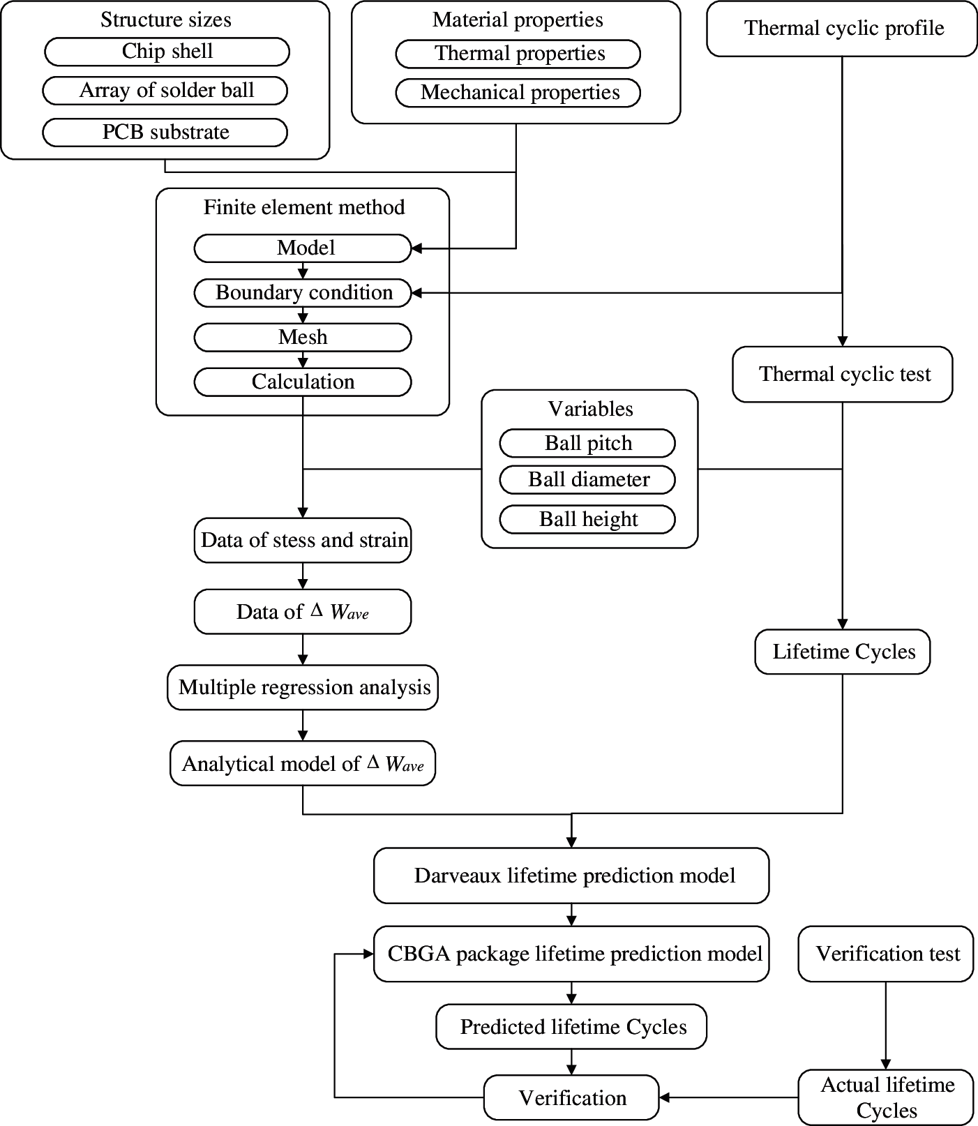
Figure 1: Procedure of lifetime prediction
At present, CBGA packages are widely used in the aerospace field due to their high-density array and ease of assembly. The structural parameters and the material properties of the CBGA packages are determined to establish the finite element model. CBGA packages typically consist of three layers. From top to bottom, the first layer is the chip, the second layer contains the solder balls and solder, and the third layer is the substrate. The structural parameters include the size of the device, the diameter of the solder ball, the pitch of the solder joint, the standoff height of the solder, and other parameters. The typical CBGA structure is shown in Fig. 2.
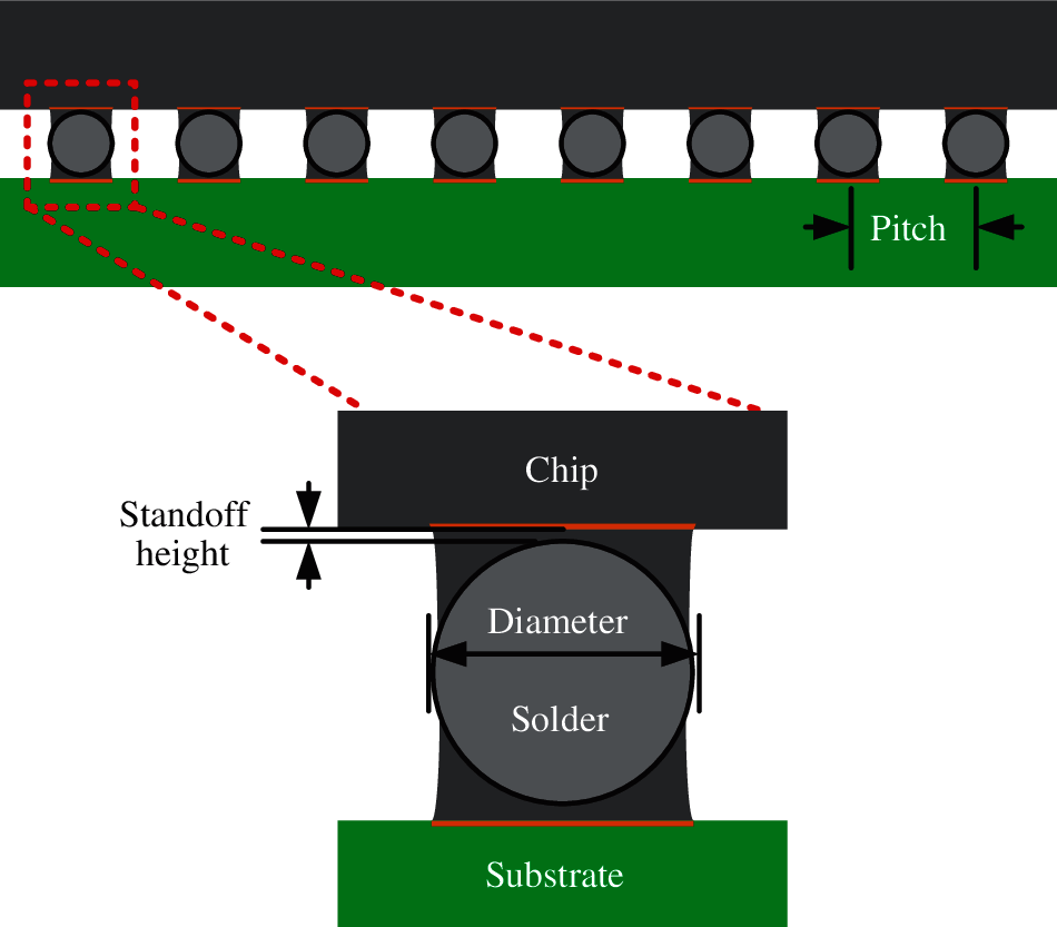
Figure 2: Schematic diagram of a CBGA package used in the finite element simulation
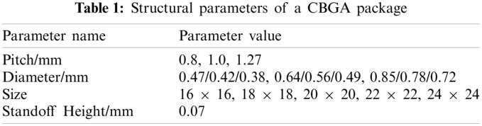
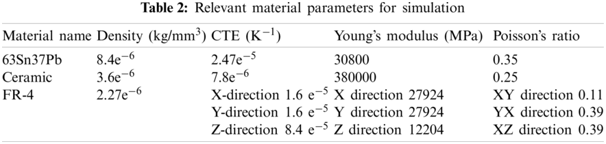
The simulation uses the typical structural parameter values used in a CBGA shown in Table 1. The material properties in this paper mainly refer to the properties related to the thermal cycle of the solder, such as Young's modulus, Poisson’s ratio, density, and thermal expansion coefficient. The packaging materials currently used in the production of CBGA are devices with ceramic shells. The solder material is 63Sn37Pb, and the PCB board is FR-4. The material properties used in the simulation are listed in Table 2.
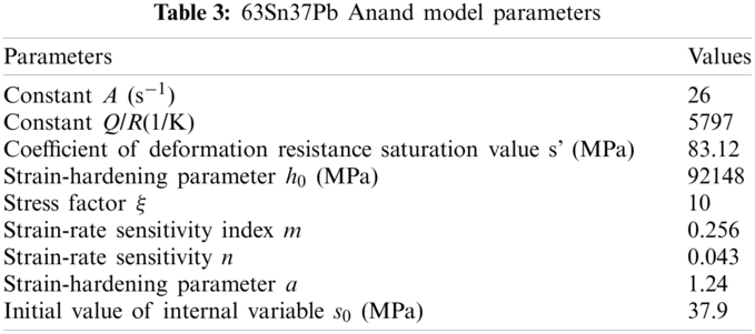
During the thermal cycle, the solder joints will creep. The Anand viscoplastic constitutive model is used to simulate the creep behavior of the solder joints. The 63Sn37Pb Anand model parameters are listed in Table 3.
The environmental parameters of the test are based on the temperature profile in the thermal cyclic test described in the ESCC-Q-70-08a standard. The temperature range is −55°C~100°C. The initial temperature is set to room temperature (22°C). The temperature change rate does not exceed 10° C/min. The maximum temperature is maintained for 15 min, and each cycle lasts 1 h. The temperature profile is shown in Fig. 3.
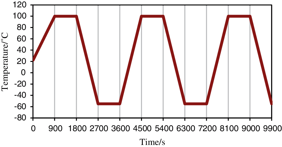
Figure 3: Temperatrue profile in the thermal cyclic test
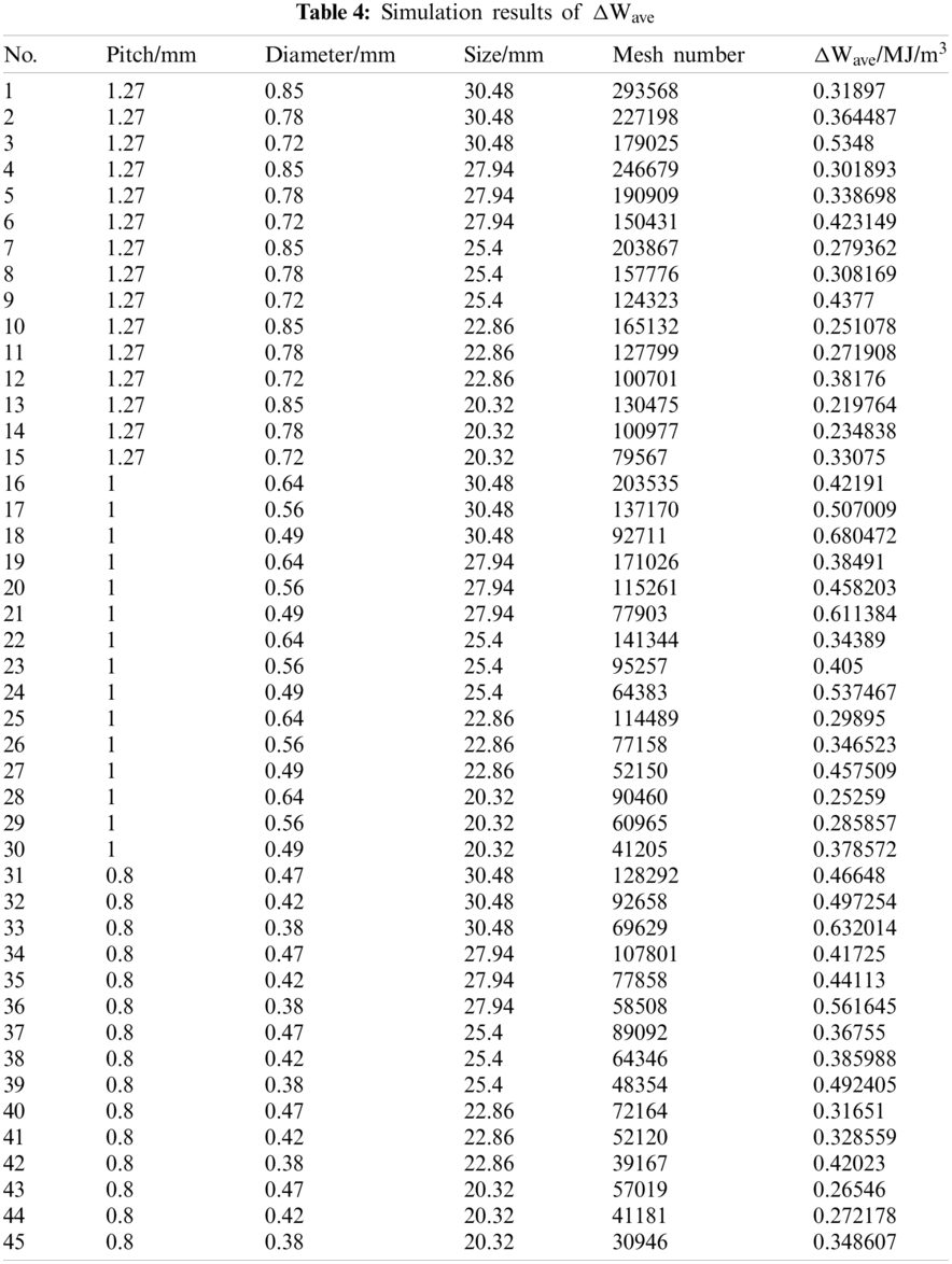
In the simulation, the model has the same temperature conditions as in the thermal cyclic test profile. Since the CBGA package is centrally symmetric, it is only necessary to establish its 1/4 finite element model, and symmetric boundary conditions are used. The bottom of the model is fixed. After setting the boundary conditions of the displacement constraints shown in Fig. 4, the thermal cyclic simulation of the CBGA model is conducted. The average mesh size of the substrate and the chip shell is 0.9 mm. The average mesh size of the solder paste is 0.15 mm. The average mesh size of the solder ball is 0.08 mm. Mesh number changes according to structural parameters, which is shown in Table 4.
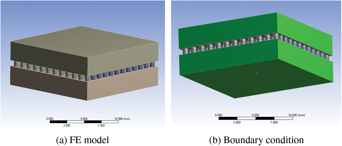
Figure 4: FE model and boundary condition
The simulation is performed with different structural parameter values to predict the lifetime of the structure. The Darveaux model is used, and ΔWave is obtained from the simulation. The average viscoplastic strain energy density Wave(n) of the previous n cycles is derived by Eq. (12). The average viscoplastic strain energy density increment ΔWave(n) is obtained from Eq. (13). Reference [32] found that ΔWave remained stable after the second thermal cycle. Therefore, the ΔWave of the third cycle is used as the result.
The simulation results indicate that the maximum stress and plastic strain occur at the corners. Hence, failure is more likely at the corners, as shown in Figs. 5 and 6. The stress is Von Mises stress. The strain is maximum principal strain. Therefore, we select a solder joint at the corner for the analysis and calculate its ΔWave. The ΔWave values of five cycles are shown in Fig. 7. It is observed that ΔWave remains stable after the second thermal cycle.
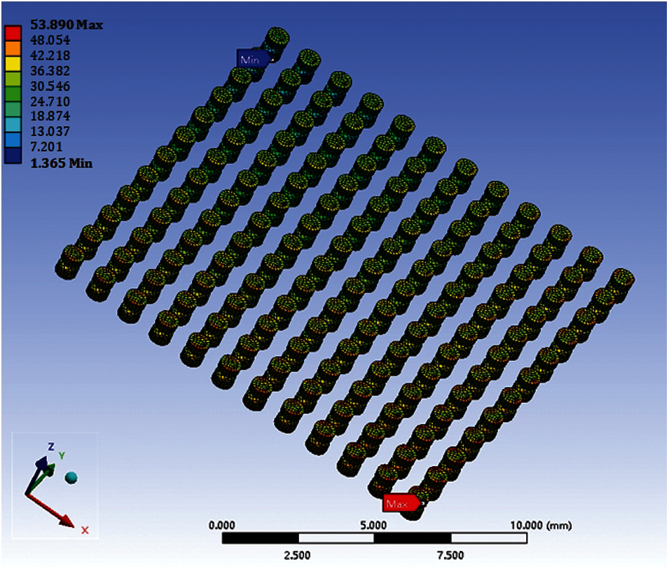
Figure 5: Stress distribution
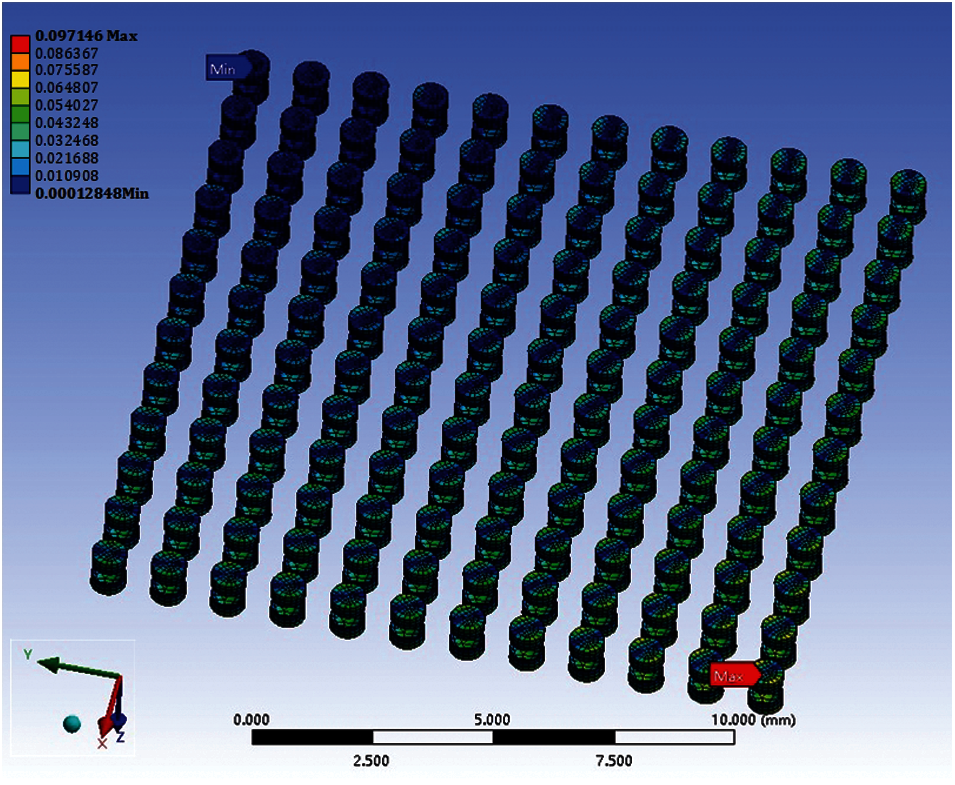
Figure 6: Plastic strain distribution
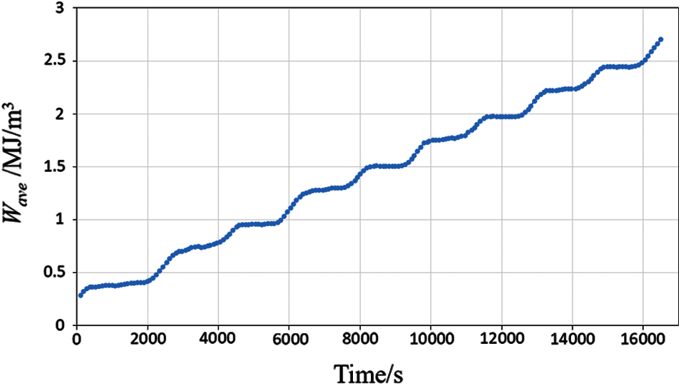
Figure 7: Wave in 5 cycles
4.1.2 Diameter of the Solder Ball
The ΔWave values for different solder ball diameters are shown in Fig. 8. ΔWave decreases with an increase in the diameter of the solder ball. The diameter affects the size of the solder ball. It is the most important parameter in the solder ball structure. The change will inevitably affect the strain energy generated by the solder ball. For larger solder balls, it is reasonable that the strain energy for the same thermal profile is smaller.

Figure 8: ΔWave vs. the diameter of the solder ball
4.1.3 Standoff Height of the Solder
The values of ΔWave for different solder standoff heights are shown in Fig. 9. ΔWave decreases with an increase in the solder standoff height, but the effect is negligible and can be ignored. Compared with the diameter, standoff height is a relatively small structural parameter in the solder ball structure. The failure of the solder ball is mainly caused by the stress in the shear direction. The change of standoff height has little effect on the tangential structure. Therefore, the influence of standoff height is small and this paper choose not to include standoff height in the analytical model of ΔWave.
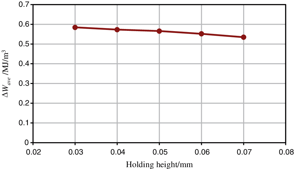
Figure 9: ΔWave vs. the standoff height of the solder
The ΔWave values for different package sizes are shown in Fig. 10. The size of the device is determined by the solder ball pitch and the size of the solder ball array. For a given solder ball pitch, ΔWave increases with an increase in the device size, and the effect is significant. When the size of packages increases, the affected area and volume under the thermal profile will increase. The strain energy increment will increase accordingly.
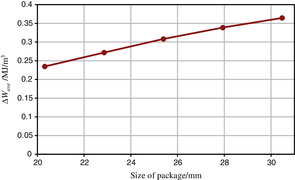
Figure 10: ΔWave vs. the package size
In addition, the pitch of the solder ball should also be considered. However, the range of the solder ball diameter depends on the pitch in practical applications. Thus, it is meaningless to determine the effect of the pitch of solder ball in the simulation.
4.2 Numerical Results of ΔWave
The ΔWave results for different values of the structural parameters and mesh numbers obtained from the simulation are listed in Table 4.
MATLAB is used to fit the simplified analytical model of ΔWave and perform multiple regression analysis for the prediction. Regression analysis provides a life prediction model with good generalization ability. The principle is to establish a prediction model that describes the distribution of the discrete sample points obtained from experiments or simulations. Commonly used regression algorithms include polynomial regression and linear regression. Multiple regression is used to predict the value and trend of the dependent variable using multiple independent variables. In addition, cross-validation is required to establish a life prediction model with a good fit and high predictability. Typically, the data are divided into a training set and a test set. In this study, the 45 sets of samples are divided into 40 sets of training data and 5 sets of test data.
According to the energy law description of the fatigue life of surface solder joints in the IPC-SM-785 standard, the potential cyclic fatigue damage is related to the structural parameters and the thermal profile. Here we use multiple nonlinear regression to fit and normalize the data as follows:
where ΔWave is the average viscoplastic strain energy density increment. p is the pitch of the solder balls. D is the diameter of the solder balls. L is the size of the package. The coefficient of determination is 0.9057, and the mean square error is 0.00766, indicating that the simplified analytical model of ΔWave has good accuracy.
5 Experimental Results and Discussion
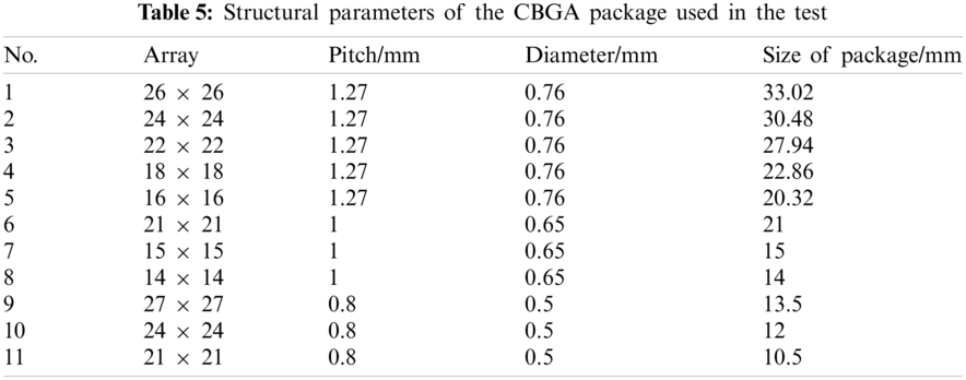
Common CBGA packages were selected for testing. The samples had different sizes, different diameters, and different solder ball pitches. CBGA575 is a large CBGA. Its structure is sensitive, and it is prone to failure. The structural parameters of the CBGA packages used in the test are listed in Table 5.
In the thermal cyclic test, a common failure monitoring method is the daisy chain monitoring system and crack length monitoring. The daisy chain system is a real-time monitoring method that determines the failure by monitoring the change in the resistance value. When any solder joint in a link cracks and fails, the resistance value of the entire link changes. The daisy chain verification system has the advantages of full coverage and straightforward analysis. The coverage rate of the solder joints tested by this method is 100%. Therefore, the daisy chain monitoring system was used as a failure monitoring method in the test to obtain the lifetime of the CBGA package sample under thermal cyclic conditions. The test equipment is shown in Fig. 11.
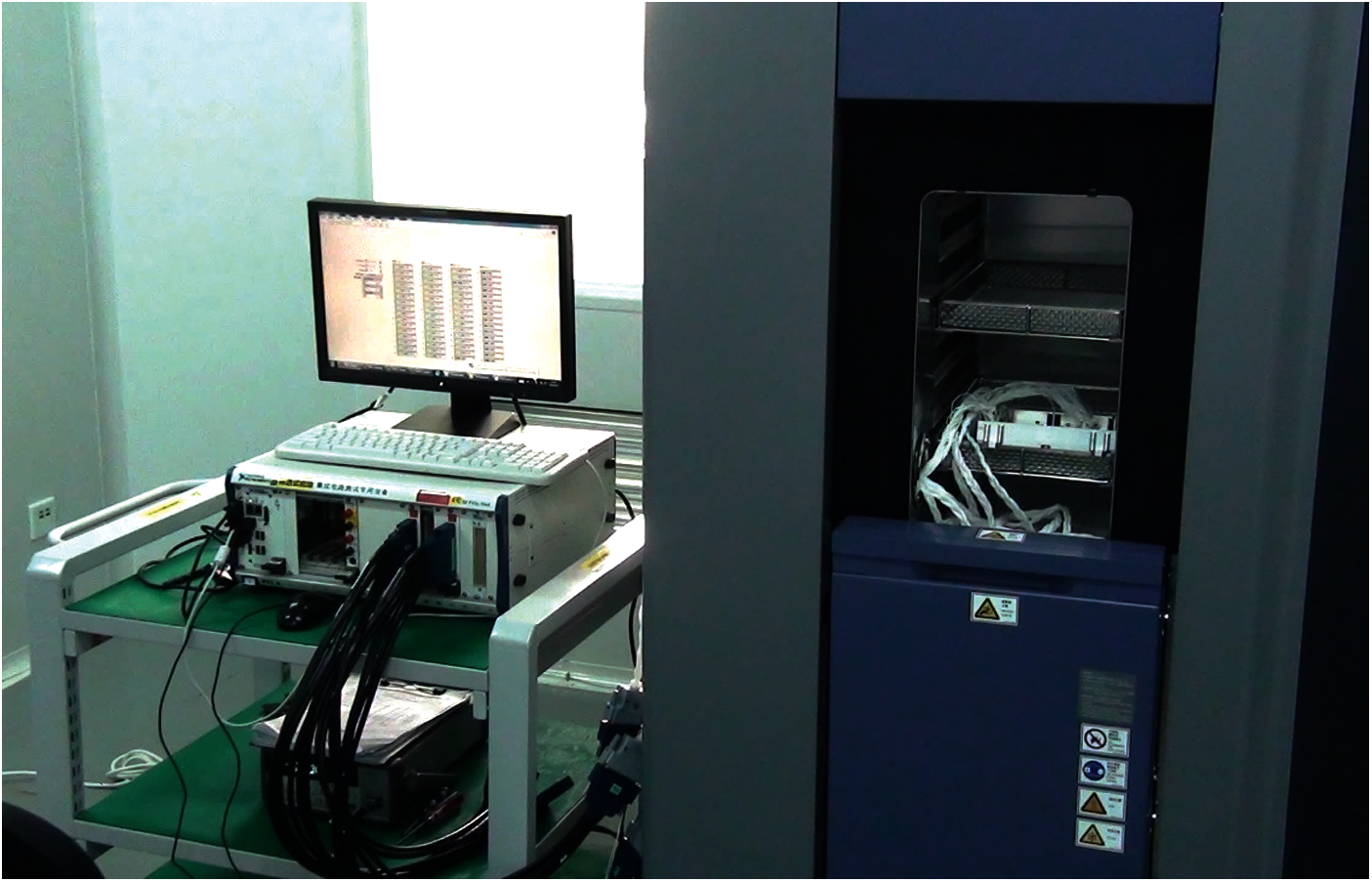
Figure 11: Test equipment
The thermal cyclic test profile shown in Fig. 3 was used. The failure criterion of the solder joint is the one used in the IPC-9701 standard. Failure is defined as two conditions. The first condition is that the event of the increase of the daisy chain resistance to 1,000 Ω for a period of one micro-second happens 10 times within 10% of the cycles to initial increase. The second condition is that the resistance increases by more than 20% within five consecutive detections.
5.2 Thermal Cyclic Test Results
During the thermal cycle test, we detect the fluctuation of the resistance of the daisy chain in real-time to evaluate the solder joint cracking of the assembly structure.
The CBGA575 sample is used as an example to illustrate the mapping of the daisy chain resistance changes and the crack growth. The first cracked solder joint we monitored was the first daisy chain link, which was located at the corner. The daisy chain resistance changes with the thermal cycle time, as shown in Fig. 12. From the first to the 235th thermal cycle, the resistance of the daisy chain remains at a normal resistance of about 3 Ω, and the solder joints are in a stable stage, as shown in Fig. 12. From the 236th to the 252nd cycle, the resistance of the daisy chain shows an increase from 20 Ω to about 300 Ω. At this time, the solder joints of the assembly structure are in the crack initiation stage, as shown in Fig. 12. Tiny cracks appear in this stage. In the high-temperature holding stage, the resistance drops to about 3 Ω, and in the low-temperature holding stage, the resistance increases to about 300 Ω. The reason is that the solder expands during the high-temperature stage. Even if the solder joints have cracked, they remain connected and have a small resistance value. As the temperature decreases, the solder shrinks, and the resistance increases. From the 253rd to the 342nd thermal cycle, the resistance of the daisy chain increases irregularly to several hundred Ω. At this time, the solder joint is in the crack propagation stage, as shown in Fig. 12. The resistance value is normal in the high-temperature stage and larger in the low-temperature stage. After the 343rd thermal cycle, the resistance of the daisy chain suddenly increases to around 50,000 Ω, exhibiting high resistance. At this time, the solder joint has completely failed, as shown in Fig. 12.
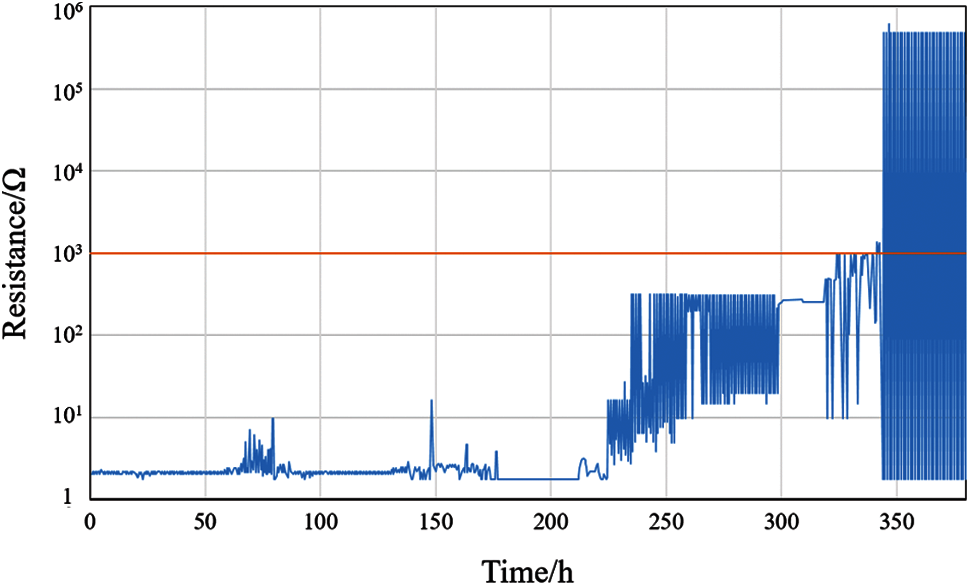
Figure 12: The daisy chain resistance change during the thermal cycling test
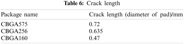
The fluctuation of the resistance of the daisy chain detected during the test indicates that the solder joints inside the assembly structure have cracked. The greater the fluctuation, the longer the cracks are between the solder joint and the component. When the high resistance state is reached for the first time, it indicates that the solder joint crack has penetrated, and the assembly structure has failed. As shown in Fig. 13, the cracks occur at the interface of the solder and pad. Hence, we assume that the crack penetration length is the same as the diameter of the interface of the solder and pad. The crack lengths are listed in Table 6, and the test results of the thermal cycle test are listed in Table 7.
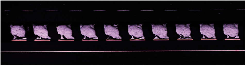
Figure 13: Graph of test samples during crack penetration
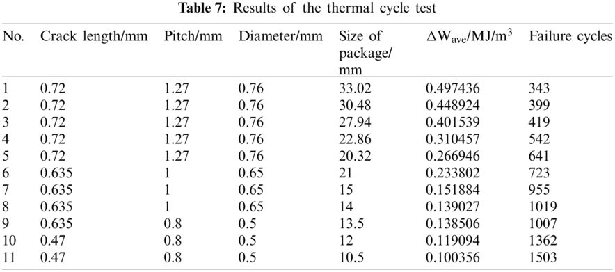
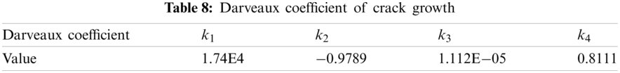
The length of the solder joint cracks and the number of failure cycles were obtained from tests, and the ΔWave values were calculated by Eq. (17). We used the nonlinear fitting function lsqnonlin in MATLAB to determine the coefficient ks of the Darveaux thermal fatigue life prediction model, i.e., the value of the coefficient ks in Eqs. (14) and (15). The modification results are listed in Table 8.
Therefore, the thermal fatigue life prediction model of the CBGA packages is proposed as follows:
where ΔWave is the average strain energy density increment, a is the crack length, and Nf is the number of failure cycles. The degree of fit between the calculated and actual results is shown in Fig. 14. The coefficient of determination is 0.9742, which indicates an excellent fit.
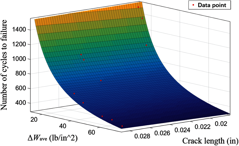
Figure 14: Fitted results of the thermal fatigue life prediction model
This paper establishes an analytical model for life prediction of CBGA Packages. It can quickly solve the lifetime of CBGA. Table 9 is the Darveaux model coefficients obtained by Li et al. [19] based on the test and simulation data of SnAgCu solder under temperature shock conditions using the least squares method. There is a considerable difference in the Darveaux model coefficients compared with this article. This shows that the coefficients of the model vary greatly for different structures, materials, and test types. Therefore, establishing a model for specific test results can make lifetime prediction results more accurate.
The improved Darveaux model is obtained by substituting Eq. (17) into Eq. (18) as follows:
We chose other CBGA575s of the same specification to verify the life prediction model. The example of daisy chain resistance change during the verification tests is shown in Fig. 15.
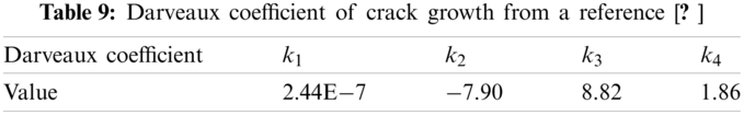
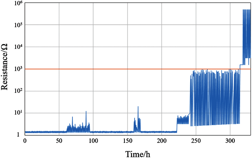
Figure 15: The example of daisy chain resistance change during the verification tests
The failure cycles of tests and the predicted failure cycles of the Darveaux model are listed in Table 10.
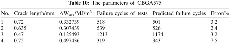
The errors between the test results and the prediction results of the Darveaux model are also shown in the table. Three of the errors are below 5%, and the other one is below 10%. They reflect the good accuracy of this life prediction model.
Simulations and experiments were used to determine the thermal fatigue lifetime of CBGA packages. A simplified analytical model of the average viscoplastic strain energy density increment ΔWave was established, and the Darveaux life prediction model of CBGA packages was modified based on the test results. After determining the structural parameters and material properties of the CBGA packages, a finite element simulation was carried out, and the ΔWave data were obtained. Subsequently, the influence of the different structural parameters on ΔWave was analyzed. Multiple regression analysis was used to establish a simplified analytical model of ΔWave using simulation data. Then, a thermal cyclic test was conducted to obtain the thermal fatigue life cycle number of typical CGBAs. We monitored the changes in the resistance value in real-time to evaluate the cracking of the solder joints of the assembly structure. The test results provided information on the thermal fatigue lifetime of typical CBGA packages and were used as part of the input into the Darveaux life prediction model. Meanwhile, the corresponding ΔWave was calculated using the simplified analytical model of ΔWave. The Darveaux life prediction model of the CBGA packages was then modified using the number of life cycles and ΔWave. The accuracy of the life prediction model of the CBGA packages was determined using a validation test. The proposed life prediction model of the CBGA packages is accurate and can be used to calculate the lifetime of CBGA packages in practical engineering applications.
Acknowledgement: The authors thank Ye Wang and Hongyan Leng of Beihang University for their thoughtful discussions and suggestions on writing and experimenting in this study.
Funding Statement: The authors received no specific funding for this study.
Conflicts of Interest: The authors declare that they have no conflicts of interest to report regarding the present study.
1. Long, X., Liu, Y., Yao, Y., Jia, F., Zhou, C. et al. (2018). Constitutive behaviour and life evaluation of solder joint under the multi-field loadings. AIP Advances, 8(8), 085001. DOI 10.1063/1.5044446. [Google Scholar] [CrossRef]
2. Pang, J., Low, T. H., Xiong, B. S., Xu, L., Neo, C. C. (2004). Thermal cycling aging effects on Sn-Ag-Cu solder joint microstructure, IMC and strength. Thin Solid Films, 462(3), 370–375. DOI 10.1016/j.tsf.2004.05.092. [Google Scholar] [CrossRef]
3. Solomon H. D. (1991). Low cycle fatigue of Sn96 solder with reference to eutectic solder and a high Pb solder. Journal of Electronic Packaging, 113(2), 102–108. DOI 10.1115/1.2905374. [Google Scholar] [CrossRef]
4. Zhang, X., Lee, S. R., Pao, Y. H. (2000). A damage evolution model for thermal fatigue analysis of solder joints. Journal of Electronic Packaging, 122(3), 200–206. DOI 10.1115/1.1286121. [Google Scholar] [CrossRef]
5. Zuo, J., Fu, G., Su, Y., Jiang, M. (2017). Thermal fatigue life analysis of defective solder joints based on engelmaier fatigue model. IEEE Electrical Design of Advanced Packaging and Systems Symposium, pp. 1–3. Haining, China. [Google Scholar]
6. Wan, B., Wang, Y., Su, Y., Fu, G. (2020). Reliability evaluation of multi-mechanism failure for semiconductor devices using physics-of-failure technique and maximum entropy principle. IEEE Access, 8, 188154–188170. DOI 10.1109/ACCESS.2020.3031022. [Google Scholar] [CrossRef]
7. Su, Y., Fu, G., Wan, B., Yu, T., Zhou, W. et al. (2019). Fatigue reliability design for metal dual inline packages under random vibration based on response surface method. Microelectronics Reliability, 100(7), 113404. DOI 10.1016/j.microrel.2019.113404. [Google Scholar] [CrossRef]
8. Wang, H., Hu, X., Jiang, X. (2020). Effects of Ni modified MWCNTs on the microstructural evolution and shear strength of Sn-3.0 Ag-0.5 Cu composite solder joints. Materials Characterization, 163, 110287. DOI 10.1016/j.matchar.2020.110287. [Google Scholar] [CrossRef]
9. Fu, G., Su, Y., Guo, W., Wan, B., Zhang, Z. et al. (2018). Life prediction methodology of system-in-package based on physics of failure. Microelectronics Reliability, 88(2), 173–178. DOI 10.1016/j.microrel.2018.06.119. [Google Scholar] [CrossRef]
10. Amagai, M., Watanabe, M., Omiya, M., Kishimoto, K., Shibuya, T. (2002). Mechanical characterization of Sn-Ag-based lead-free solders. Microelectronics Reliability, 42(6), 951–966. DOI 10.1016/S0026-2714(02)00017-3. [Google Scholar] [CrossRef]
11. Xu, C., Gang, C., Sakane, M. (2005). Prediction of stress–strain relationship with an improved Anand constitutive model for lead-free solder Sn-3.5Ag. IEEE Transactions on Components & Packaging Technologies, 28(1), 111–116. DOI 10.1109/TCAPT.2004.843157. [Google Scholar] [CrossRef]
12. Chen, X., Chen, G., Sakane, M. (2004). Modified Anand constitutive model for lead-free solder Sn-3.5Ag. Conference on Thermal & Thermomechanical Phenomena in Electronic Systems, pp. 447–452. Piscataway: IEEE. [Google Scholar]
13. Wu, J., Yang, H., Zhang, Y. (2018). The research of low temperature sintering nano-sliver paste based on Anand model. Proceedings of the International Symposium on Big Data and Artificial Intelligence, pp. 105–108. Hong Kong: Association for Computing Machinery. [Google Scholar]
14. Long, X., He, X., Yao, Y. (2017). An improved unified creep-plasticity model for SnAgCu solder under a wide range of strain rates. Journal of Materials Science, 52(10), 6120–6137. DOI 10.1007/s10853-017-0851-x. [Google Scholar] [CrossRef]
15. Wang, W. J., Long, X., Du, C. Y., Fu, Y. H., Wu, Y. P. (2020). Enhancement of the unified constitutive model for viscoplastic solders in wide strain rate and temperature ranges. Strength of Materials, 51(8), 917–925. DOI 10.1007/s11223-020-00142-5. [Google Scholar] [CrossRef]
16. Long, X., Chen, Z., Wang, W., Fu, Y., Wu, Y. (2020). Parameterized Anand constitutive model under a wide range of temperature and strain rate: Experimental and theoretical studies. Journal of Materials Science, 55(24), 10811–10823. DOI 10.1007/s10853-020-04689-1. [Google Scholar] [CrossRef]
17. Che, F. X., Pang, J. H. (2012). Fatigue reliability analysis of Sn-Ag-Cu solder joints subject to thermal cycling. IEEE Transactions on Device and Materials Reliability, 13(1), 36–49. DOI 10.1109/TDMR.2012.2195007. [Google Scholar] [CrossRef]
18. Wang, W., Chen, Z., Wang, S., Long, X. (2020). Mechanics-based acceleration for estimating thermal fatigue life of electronic packaging structure. Microelectronics Reliability, 107(4), 113616. DOI 10.1016/j.microrel.2020.113616. [Google Scholar] [CrossRef]
19. Li, J., Xu, H., Hokka, J., Mattila, T. T., Chen, H. et al. (2011). Finite element analyses and lifetime predictions for SnAgCu solder interconnections in thermal shock tests. Soldering & Surface Mount Technology, 23(3), 161–167. DOI 10.1108/09540911111146917. [Google Scholar] [CrossRef]
20. Jiang, L., Zhu, W., He, H. (2017). Comparison of Darveaux model and Coffin-Manson model for fatigue life prediction of BGA solder joints. International Conference on Electronic Packaging Technology, pp. 1474–1477. Piscataway: IEEE. [Google Scholar]
21. Hu, W., Li, Y., Sun, Y., Mosleh, A. (2016). A model of BGA thermal fatigue life prediction considering load sequence effects. Materials, 9(10), 860. DOI 10.3390/ma9100860. [Google Scholar] [CrossRef]
22. Lee, S. R., Ben, H., Kong, Y. H., Baylon, B., Leung, T. et al. (2002). Assessment of board level solder joint reliability for PBGA assemblies with lead-free solders. Soldering & Surface Mount Technology, 14(3), 46–50. DOI 10.1108/09540910210444728. [Google Scholar] [CrossRef]
23. Akay, H. U., Liu, Y., Rassaian, M. (2003). Simplification of finite element models for thermal fatigue life prediction of PBGA packages. Journal of Electronic Packaging, 125(3), 347–353. DOI 10.1115/1.1569956. [Google Scholar] [CrossRef]
24. Liang, J., Gollhardt, N., Lee, P. S., Heinrich, S., Schroeder, S. (1997). An integrated fatigue life prediction methodology for optimum design and reliability assessment of solder interconnections. Pacific Rim/ASME International and Intersociety Conference, Electronic and Photonic Packaging, pp. 1583–1592. Kohala Coast, HI: ASME. [Google Scholar]
25. Darveaux, R. (2000). Effect of simulation methodology on solder joint crack growth correlation. Proceedings of the 50th Electronic Components and Technology Conference, pp. 1048–1058. Las Vegas. [Google Scholar]
26. Chen, R. S., Huang, C. H., Xie, Y. Z. (2012). Application of optimal design on twin die stacked package by reliability indicator of average SED concept. Journal of Mechanics, 28(1), 135–142. DOI 10.1017/jmech.2012.14. [Google Scholar] [CrossRef]
27. Li, L. T., Jing, B., Hu, J. X. (2020). The degradation study for QFP interconnection structure based on PCMD health index and Darveaux model. Microelectronics Reliability, 109(11), 113662. DOI 10.1016/j.microrel.2020.113662. [Google Scholar] [CrossRef]
28. Marbut, C. J., Montazeri, M., Huitink, D. R. (2018). Rapid solder interconnect fatigue life test methodology for predicting thermomechanical reliability. IEEE Transactions on Device and Materials Reliability, 18(3), 412–421. DOI 10.1109/TDMR.2018.2851541. [Google Scholar] [CrossRef]
29. Sitta, A., Mauromicale, G., Sequenzia, G., Messina, A. A., Renna, M. et al. (2021). Thermo-mechanical finite element simulation and visco-plastic solder fatigue for low voltage discrete package. 22nd International Conference on Thermal, Mechanical and Multi-Physics Simulation and Experiments in Microelectronics and Microsystems (EuroSimE), pp. 1–6. St. Julian. [Google Scholar]
30. Zhang, X., Wong, E. H., Lee, C., Chai, T. C., Ma, Y. et al. (2004). Thermo-mechanical finite element analysis in a multichip build up substrate based package design. Microelectronics Reliability, 44(4), 611–619. DOI 10.1016/j.microrel.2003.09.006. [Google Scholar] [CrossRef]
31. Anand, L. (1982). Constitutive equations for the rate-dependent deformation of metals at elevated temperatures. Transactions of the Asme Journal of Engineering Materials & Technology, 104(1), 12–17. DOI 10.1115/1.3225028. [Google Scholar] [CrossRef]
32. Dauksher, W., Lau, J. (2009). A finite-element-based solder-joint fatigue-life prediction methodology for Sn-Ag–Cu ball-grid-array packages. IEEE Transactions on Device and Materials Reliability, 9(2), 231–236. DOI 10.1109/TDMR.2009.2014943. [Google Scholar] [CrossRef]
 | This work is licensed under a Creative Commons Attribution 4.0 International License, which permits unrestricted use, distribution, and reproduction in any medium, provided the original work is properly cited. |