| Computer Modeling in Engineering & Sciences |
DOI: 10.32604/cmes.2021.016756
ARTICLE
Geometrically-Compatible Dislocation Pattern and Modeling of Crystal Plasticity in Body-Centered Cubic (BCC) Crystal at Micron Scale
Dedicated to Professor Karl Stark Pister for his 95th birthday
Department of Civil and Environmental Engineering, The University of California, Berkeley, CA 94720, USA
*Corresponding Author: Shaofan Li. Email: shaofan@berkeley.edu
Received: 24 March 2021; Accepted: 03 June 2021
Abstract: The microstructure of crystal defects, e.g., dislocation patterns, are not arbitrary, and it is possible that some of them may be related to the microstructure of crystals itself, i.e., the lattice structure. We call those dislocation patterns or substructures that are related to the corresponding crystal microstructure as the Geometrically Compatible Dislocation Patterns (GCDP). Based on this notion, we have developed a Multiscale Crystal Defect Dynamics (MCDD) to model crystal plasticity without or with minimum empiricism. In this work, we employ the multiscale dislocation pattern dynamics, i.e., MCDD, to simulate crystal plasticity in body-centered cubic (BCC) single crystals, mainly α-phase Tantalum (α-Ta) single crystals. The main novelties of the work are: (1) We have successfully simulated crystal plasticity at micron scale without any empirical parameter inputs; (2) We have successfully employed MCDD to perform direct numerical simulation of inelastic hysteresis of the BCC crystal; (3) We have used MCDD crystal plasticity model to demonstrate the size-effect of crystal plasticity and (4) We have captured cross-slip which may lead to size-effect.
Keywords: α-phase tantalum; BCC crystal; crystal plasticity; dislocation pattern dynamics; multiscale simulation; size effect
Crystal plasticity is a very common physical phenomenon. The origin of crystal plasticity is crystal dislocation motion and evolution. However, the crystal plasticity is resulted from aggregated dislocation motions, i.e., motion of dislocation pattern, rather than the motion of a single dislocation. It is because not only dislocation itself but also mutual interaction and evolution of assemble dislocations influence plastic behavior in crystalline materials. Therefore, the massive number of dislocations assembling in some specific regions in crystalline materials so that studying statistical variables from the aggregation is the only feasible way.
Based on various topological grouping of dislocations, some dislocation patterns have specific names. For example, we usually name the “wall-shape” dislocations as dislocation cells, the “strip-shape” dislocations as veins and mutually crossed “grid-shape” as dislocation labyrinth. According to past studies on crystal plasticity, many plastic phenomena in crystalline materials are strongly influenced by those micro-defects.
Recently, Li et al. [1–4] have proposed and developed a Multiscale Crystal Dislocation Dynamics (MCDD) method in which a physics-informed mesh is proposed and an atomistic-informed constitutive model and strain gradient-based atomistic kinematic rule are applied. Differen from phenomenological models, this method is an atom-level first principle method, i.e., there are no non-physical parameters to be fitted and inelastic behavior of crystalline materials are modelled by crystal lattice-dependent mesh and nonlinear kinematic rule so that this method can directly reflect essences of plasticity in crystalline materials. Besides, compared to Molecular Dynamics (MD) or Density-functional Theory (DFT), the crystal lattice-dependent mesh is a coarse-grained meshing method which can be scaled up to form mesoscale or even microscale models. Therefore, computational efficiency of the MCDD is much higher than MD and DFT. More importantly, a novel physical concept of geometrically compatible dislocation pattern (GCDP) is proposed to link the crystal lattice-dependent mesh and real topological structures of dislocation patterns in crystalline materials at least in early phase of crystal plasticity. This is because the initial dislocation formation or crystal defect always occurs on a lattice plane as forms of lattice complex (simplicial complex), it is reasonable to postulate that their aggregation will form a dual lattice complex, or CW complex [5,2]. In algebraic topology, a CW complex is an abbreviation for “Closure-finite Weak topology” complex, which is a kind of the Hausdorff space that can be partitioned into many open cells. In a CW complex, a simplex σk is homeomorphic to
In this work, we use the concept of CW complex to construct geometrically compatible dislocation patterns, and such as a class of specific geometric objects, geometrically compatible dislocation patterns, have only been occasionally mentioned or reported in the literature, e.g., [5,6] but without systematical studies.
Tantalum, as lustrous transition metal, is a highly corrosion-resistant material, and it is widely used as minor components in many alloys, as part of the refractory metals group. In current industry applications, tantalum is mainly used in following four fields: capacitors, chemical industry, alloy and hard metals [7,8,9]. Due to its excellent corrosion resistance to oxide layer, tantalum can be applied to components manufactured for installations under corrosion attack, such as heat exchangers, heating spark plugs, coolers, pipes and coatings for vessels in chemical engineering. In superalloys, i.e., alloys based on nickel, cobalt and iron-nickel, introduction of tantalum improves the corrosion resistance, increases grain finesse, makes carbon stable and improves hardness and strength. Tantalum oxide has high dielectric coefficient and good stability. Therefore, tantalum can be manufactured as powder, wire, foil and coatings in capacitors. Besides, the hard metals industry consumes about 30% tantalum production. Tantalum is used in mixed carbides addition which can improve the erosion resistance, hot strength, hardness, ultimate bending strength, toughness, shock resistance and grain refinement.
In present work, we employed the multiscale crystal defect dynamics, or the geometrically-compatible dislocation pattern dynamics, to investigate the crystal plasticity of a special BCC crystal–α-Tantalum at micron scale (up to 3 μm × 3 μm × 6 μm) to provide further validation of MCDD method. Furthermore, we have used MCDD to investigated the size effect of crystal plasticity in the study of crystal plasticity of single crystal α-Ta.
The rest of the paper is organized as follows: based on algebraic topology, construction of crystal lattice-dependent mesh and resemblance between the physics-informed mesh and real dislocation patterns will be discussed in Section 2. Then the atom-level first principled constitutive model for single Tantalum is presented in Section 3. In Section 4, the strain gradient based nonlinear kinematic rule are demonstrated. And the numerical examples are provided in Section 5. We conclude the study with summaries and comments in Section 6.
In this section, we first introduce the dual lattice tessellation to partition a BCC crystal into a finite element mesh of lattice process zones, which was proposed in [1]. Then we shall discuss how to use discrete exterior calculus and algebraic topology to offer mathematical description of process zone tessellation [2]. Finally by introducing the notion of geometrically-compatible dislocation pattern, we give the physical meaning of the lattice process zone, which are the generic dislocation patterns [3,4].
2.1 Dual Lattice Process Zone Model
In discrete dislocation dynamics (DD), the smallest unit of dislocation dynamics is the dislocation segment [10]. Different from dislocation dynamics, the smallest unit of dislocation pattern dynamics is discrete dislocation pattern. To start with, we need first to construct dislocation pattern elements in a crystal lattice space.
To identify the generic dislocation pattern for a given lattice structure, we need first to construct a Voronoi cell for an representative atom: placing planes normal to line segments formed by two neighboring atoms of lattice complex at midpoints. These truncation planes will form a convex polyhedron around the representative atom, and the convex polyhedron is called the Wigner-Seitz cell in crystallography for Bravais lattices. Using the terminology of crystal chemistry, we may call it as the Voronoi-Dirichelt Polyhedron (VDP). However, VDP is a bigger set of unit cells that includes the Wigner-Seitz cell. This is because different choice of representative atoms will lead to different shape of VDP. For our current BCC model, we choose the nearest 8 atoms and the second nearest 6 atoms as representative atoms. Therefore, the corresponding VDP is a truncated octahedron or the standard Wigner-Seitz cell for the BCC lattice as shown in Fig. 1a.
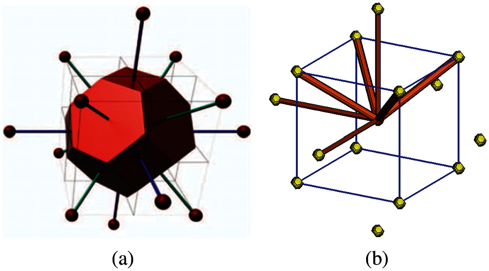
Figure 1: (a) A BCC Wigner-Seitz cell and (b) One third-order process zone and 14 s-order process zone
The complete steps to have dual lattice process zone tessellation:
(1) Based on crystal lattices of whole atoms in 2D or 3D space, we can have correspondingdual lattice;
(2) Then we shall scale the VDPs down, put them at atom positions and term it as the highestorder process zone element;
(3) It is found that the whole two-dimensional or three-dimensional space cannot be coveredby the scaled VDP. Therefore, corresponding different shape of elements are used to fill inthe gaps among scaled VDP. Therefore, for BCC crystal lattice, Fig. 1b shows two typesof prism elements (hexagonal cross section and square cross section). Figs. 2a–2f show theconnections of prism element-to-truncated octahedron element and prism element-to-wedge element. Figs. 2g–2l show the connections of prism element-to-tetrahedron element.
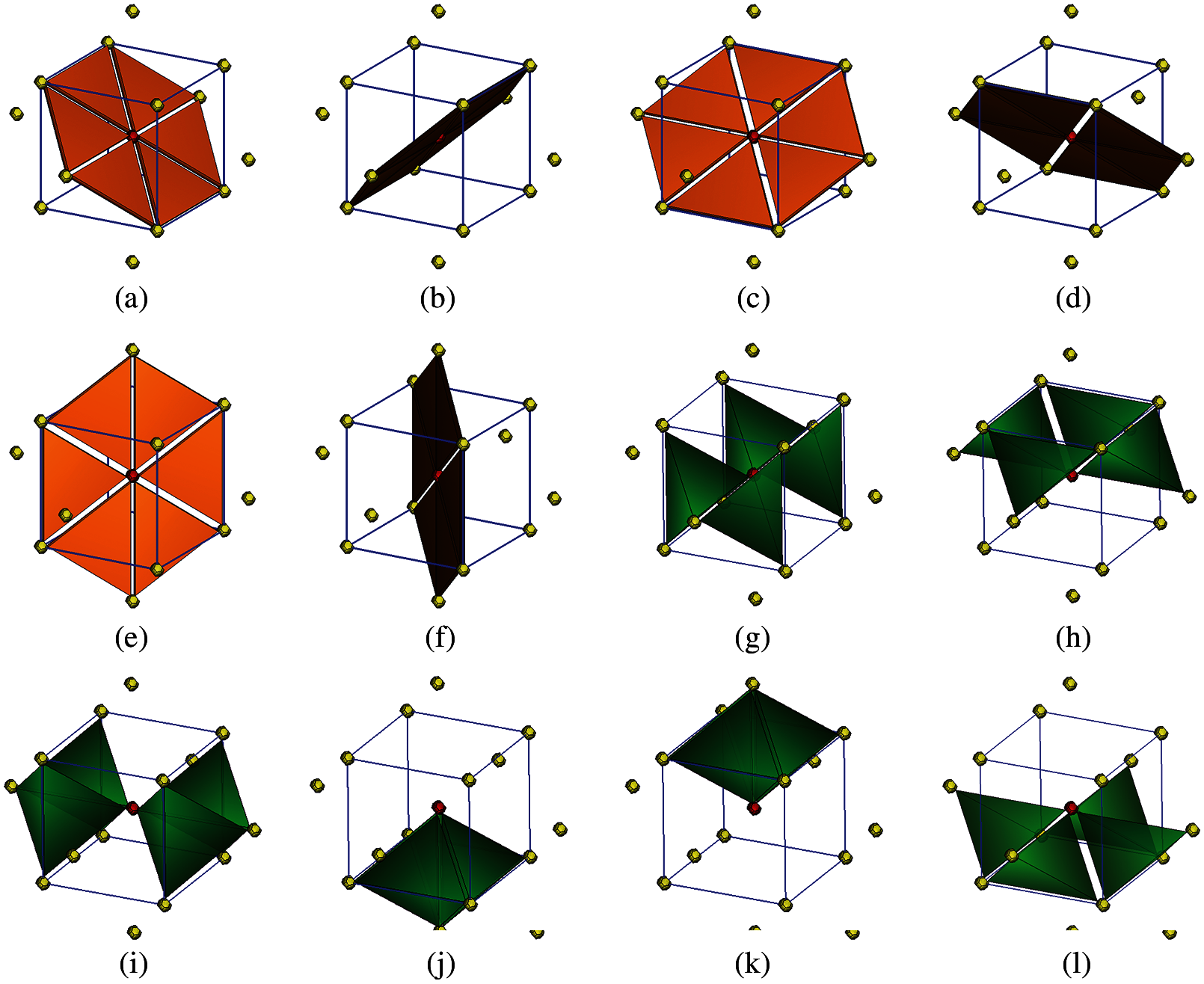
Figure 2: (a) There are six slip planes and 36 first-order process zone elements ((a)--(f)); and 24 bulk tetrahedron elements ((g)--(l)) in a BCC super dual-lattice unit cell
Therefore, in a BCC dual-lattice unit, we have (1) one 3rd order process zone, i.e., scaled down truncated octahedron element; (2) fourteen 2nd order process zone elements including 8 hexagonal prism elements and 6 square prism elements; (3) thirty-six 1st process zone elements; (4) twenty-four tetrahedron elements.
2.2 Exterior Calculus Representation on BCC Lattice Complex
Inspired from Ariza et al. [11], we also follow the concepts and terminology in algebraic topology [12,13] and give quantitative description of super dual lattice complex in BCC crystals.
Different from Ariza and Ortiz's work, the present work is about dislocation pattern dynamics, and we cannot use simplicial complex p-cell to describe discrete dislocation pattern units. However, we still found that the mathematical theory of algebraic topology and exterior differential calculus can also applied to describe dislocation pattern dynamics in terms of p-cell of CW complexes. In this work, we introduce following cell index system to label points, edges, faces and volumes in different discrete dislocation pattern units, i.e., truncated octahedron elements, prism elements, wedge elements and tetrahedron elements. We use a unified symbol,
In the next we shall take
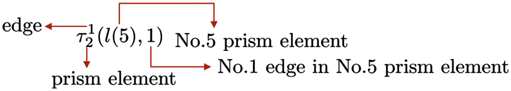
Figure 3: Polytopal labeling
This labeling process is important in finite element method (FEM) formulation and implementation, because we need to use the exterior calculus symbol to construct the connectivity array of FEM code that maps the local indices into global indices.
By using boundary operator of exterior calculus, we can represent lines and faces. For example, as shown in Fig. 6, for central scaled truncated octahedron
and
which are shown in Fig. 4
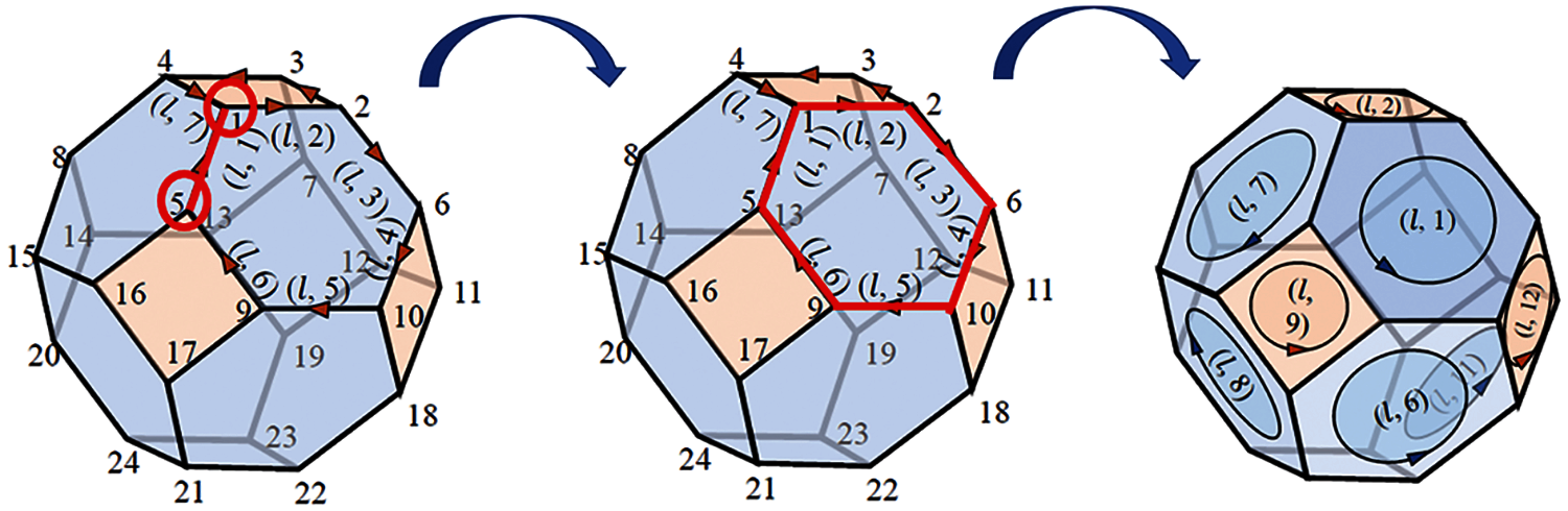
Figure 4: Boundary operator illustration:from vertex to edge, from edge to surface, from surface to volume
Similarly, we can use co-boundary operator δ to help us understand the relations among different types of elements. For example, for the central scaled truncated octahedron
which established the links from vertex to edge, edge to surface and surface to volume as shown in Fig. 5.
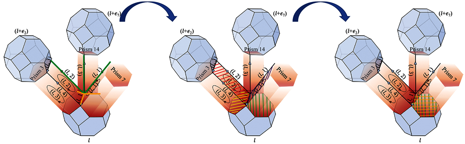
Figure 5: Co-boundary operator illustration: from vertex to edge, from edge to surface, from surface to volume
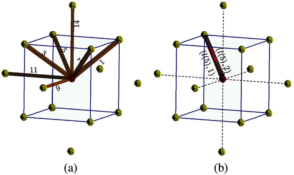
Figure 6: Lattice complex representation of the BCC lattice and indexing scheme: (a) 2nd-order process zone elements and (b) the prism element No. 5
Furthermore, we can also apply the cell complex notation defined above to represent other types of elements. For example, the prism element
in which,
2.3 Geometrically Compatible Dislocation Pattern
In Lyu et al.’s work [3], an innovative concept, Geometrically-compatible dislocation pattern (GCDP) that offers a physical foundation of pre-dislocation pattern mesh. As Lyu et al.’s work, in this section we give geometrically-compatible dislocation pattern formation of BCC crystal structure.
Since we know that body-centered cubic (BCC) crystal structure is NOT the closed-packed structure, the most likely slip plane should be
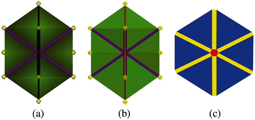
Figure 7: BCC (110) plane projection of DLPZ tilling. (a) 3D dual-lattice process zone unit cell of BCC crystal (b) The projection of 3D dual-lattice process zone unit cell onto (110) plane (c) 2D geometrically-compatible dislocation pattern
From the projection from 3D to 2D, we understand that 2D triangle bulk element is actually the projection of the first-order process zone element in 3D DLPZ tilling, rather than the projection of 3D tetrahedron bulk crystal element; the projection of the second-order process zone element (prism element) in
Since we have the two-dimensional geometrically-compatible dislocation pattern as in Fig. 7c, we can have the following scenario of dislocation pattern formation process in body-centered cubic materials. At the very beginning stage of the dislocation multiplication, statistical number of parallel slips have pre-existed in different slip systems along different atomic planes, and those parallel slips will converge to a bulk junction as shown in Fig. 8. From energetic perspective, maintaining geometric compatibility and local crystal structure integrity may be a necessity for deformed crystal, therefore these parallel slip planes in different slip systems must form a stable and geometrically-compatible dislocation networks. We call the networks as geometrically-compatible dislocation pattern (GCDP) (see Fig. 8c). Therefore, we identify the geometrically-compatible dislocation pattern as substructures that have the shape of the Wigner-Seitz cell of the original crystal lattice.
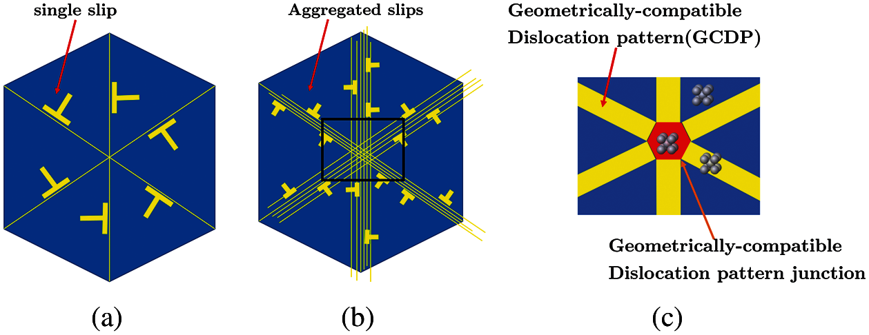
Figure 8: Illustration of a possible formation of a two-dimensional geometrically-compatible dislocation pattern: (a) Dislocations in slip planes, (b) Aggregated parallel slips in multiple slip systems converge to a bulk junction, and (c) A two-dimensional geometrically-compatible dislocation pattern
3 Atomistic-Informed Constitutive Relation
3.1 Embedded-Atom Potentials for BCC
The embedded-atom model (EAM) is widely used atomistic potential model for metals in molecular dynamics, which takes into account interactions between atom nucleus as well as electron density contribution. The EAM method has been extensively used in molecular dynamics for metallic materials,
Based on general formulation of EAM [14,15], the EAM potential could be written as:
in which, ϕ (rij) is the nucleus pair interaction energy, F is the electron embedding energy,
where
Based on EAM formulation and stress-work conjugate relation, we can have a fourth-order elastic tensor formulation:
The macroscale constitutive relation is expressed in terms of several important stress measures as follows:
in which P is the first Piola-Kirchhoff stress, S is the second Piola-Kirchhoff stress and σ is the Cauchy stress, Ωu0 is the volume of crystal unit cell in the referential configuration, ωu is the volume of crystal unit cell in the spatial configuration, R is the undeformed atom bond, r is the deformed atom bond, F is deformation gradient in the crystal unit cell and W is the strain energy density of the crystal unit cell, nb represents the number of neighboring atoms in the crystal unit cell.
To find the initial equilibrium state for many-body potential problem, we use the general or generic analytical form of EAM potential reported in literature. To find the initial equilibrium state, we first consider the
Based on Eq. (11), we can compute the equilibrium lattice constant a, which satisfies the initial equilibrium condition. Thus it becomes an optimization problem with one variable and we firstly find the derivative of norm of S about lattice constant a:
To solve this nonlinear equation, we use the Newton-Raphson method to linearize the above equation,
Therefore, we can obtain the i-th iteration result ai as:
the iterative solution stops when until δ ai < tol.
The analytical expression of
in which
We use three hierarchical order strain gradients to model them (Eqs. (16), (17)),
where x represents deformed material point coordinates in spatial configuration, X represents the initial material point coordinates in referential configuration.
Then the bond vectors in corresponding dislocation pattern segments may be defined by the higher order Cauchy-Born model as follows:
respectively. Subsequently, as a function of deformation gradients, the strain energy density Ww, Wp, and Wt of the corresponding dislocation pattern elements under consideration, which can be expressed as follows:
The constitutive relations in wedge, prism and truncated octahedron (tetradecahedron) elements can be further explicated as follows:
in which P is the first Piola-Kirchhoff stress, which is coupled with the deformation gradient F; Q is the second-order stress coupled with the 1st-order strain gradient G; U is the third-order stress coupled with the 2nd-order strain gradient H, and V is the fourth-order stress coupled with the 3rd-order strain gradient K.
The higher order stress tensor are expressed in a general form as:
4 MCDD Finite Element Formulation
To formulate MCDD finite element formulation, we first consider the Hamilton principle in terms of displacement variation for a fixed time interval as:
in which,
The variation of the kinetic energy of the crystal is:
The internal virtual work of the crystal is:
and the external virtual work of the crystal is:
Substituting these formulas above into the Hamilton principle, we can have Galerkin weak form of Multiscale Crystal Defects Dynamics for a crystal as shown as follows:
Considering finite element discretization and interpolation,
where Bi(X) is the finite element shape function, and ui are the element nodal displacements, we can rewrite the form of considering different types of elements as:
where b is the body force,
Note that based on internal virtual work,
the successive integration by parts yields the following expression:
In our current MCDD FLEM model, we assume that on the boundary of the crystalline solid the higher order stress effects are negligible, i.e.,
This is a very coarse approximation, and further work is needed to consider higher order strain gradient traction boundary condition.
5.1 Uniaxial Tension and Pure Shear Tests
In this section, we first present MCDD numerical results in uniaxial tension and pure shear tests. To model and simulate crystal plasticity in α-phase tantalum crystal, we adopt the higher order Cauchy-Born rule that utilizes the Embedded-Atom method potential discussed in [15].
The total energy E of the crystal solid can be written as:
where ϕ (rij) represents the pair energy between atoms i and j separated by a distance rij, and Fi is the embedding energy associated with embedding an atom i into a local site with an electron density
with ρj(rij) as the electron density at the site of atom i arising from atom j at a distance rij away.
We use the following pair potential ϕ(r) for α-Ta,
where re is the equilibrium spacing between nearest neighbors, A,B,α and β are four adjustable parameters, and κ and λ are two additional parameters for the cutoff. The electron density ρ(r) is defined as:
The embedding energy function is expressed as follows:
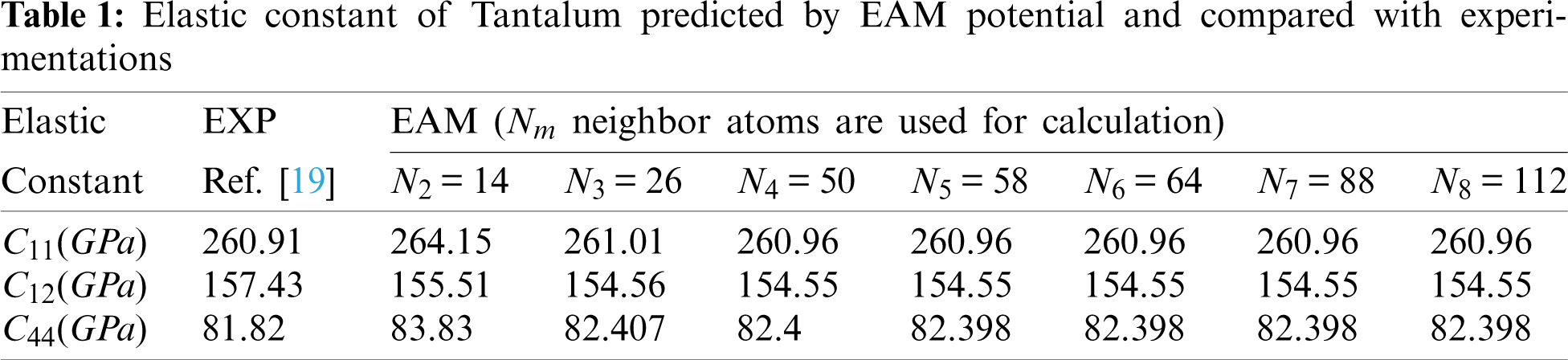
The value of parameters used for α-phase Tantalum are taken from in [18]. Based on the EAM formulation, i.e., Eq. (9), we first calculate elastic modulus of the crystal and compare it with experimental results, and the results are listed in Appendix Table A1.
The MCDD model with the size of
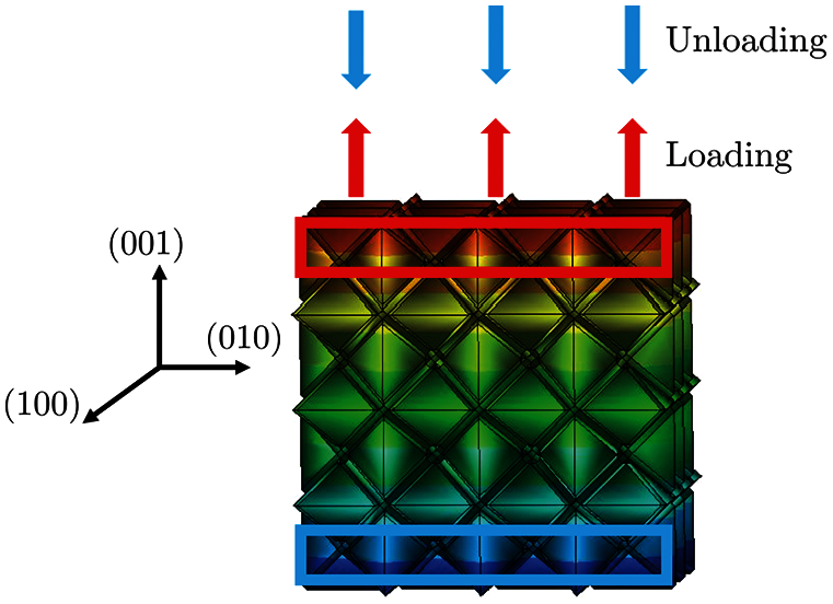
Figure 9: MCDD modeling and simulation of a BCC crystal under uniaxial tension/compression loadings
Meanwhile, molecular dynamics (MD) simulation is conducted by using the Large-scale Atomic/Molecular Massively Parallel Simulator (LAMMPS), which is a popular open-source molecular dynamics simulation software package. The MD model or specimen has 59582 atoms. The atomic pair potential for α-Ta is based the reference [15]. The same strain rate used in MCDD calculations is applied in MD simulations.
By choosing the unloading position at three different strain marks mentioned above, we have obtained the corresponding stress-strain relations in MCDD simulations. The obtained stress-strain relations are compared with those of MD simulations as shown in Fig. 10, respectively. From Fig. 10, one may find that in all three loading/unloading cases the stress-strain relations obtained from MCDD simulations and from MD simulations are consistent, which indicates the MCDD method is valid in simulating nanoscale crystal plasticity for single α-Ta crystal.
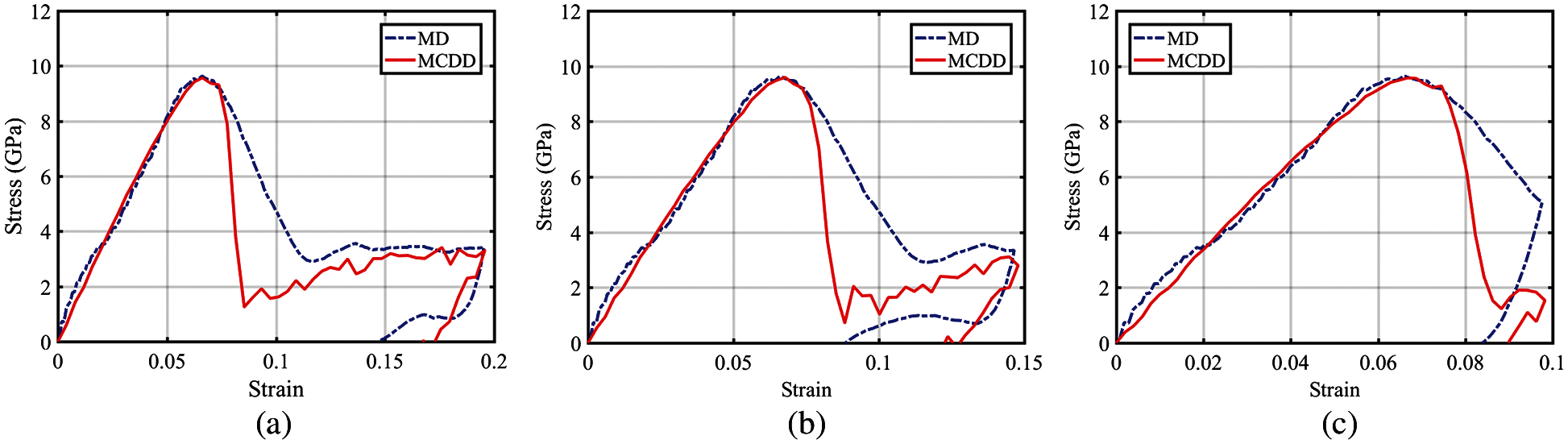
Figure 10: Stress-strain relations for three unloading strains: (a) 20%. (b) 15%. (c) 10% under loading and unloading
By considering higher order Cauchy-Born rule based higher order strain gradient formulations on wedge shaped dislocation patterns, prism shaped dislocation patterns, and truncated octahedron dislocation patterns, the MCDD method shows its ability to capture inelastic behavior and the path-dependent constitutive relation of α-phase tantalum in single crystal plasticity simulation. Fig. 11 shows the von-Mise stress contours on (100) and (010) planes. It is remarkable that the above crystal plasticity simulation is based on local “higher order hyperelastic strain gradient formulation”. Moreover, the above MCDD simulation has much computational efficiency in comparison with the MD model or specimen with the same size and boundary and loading conditions.
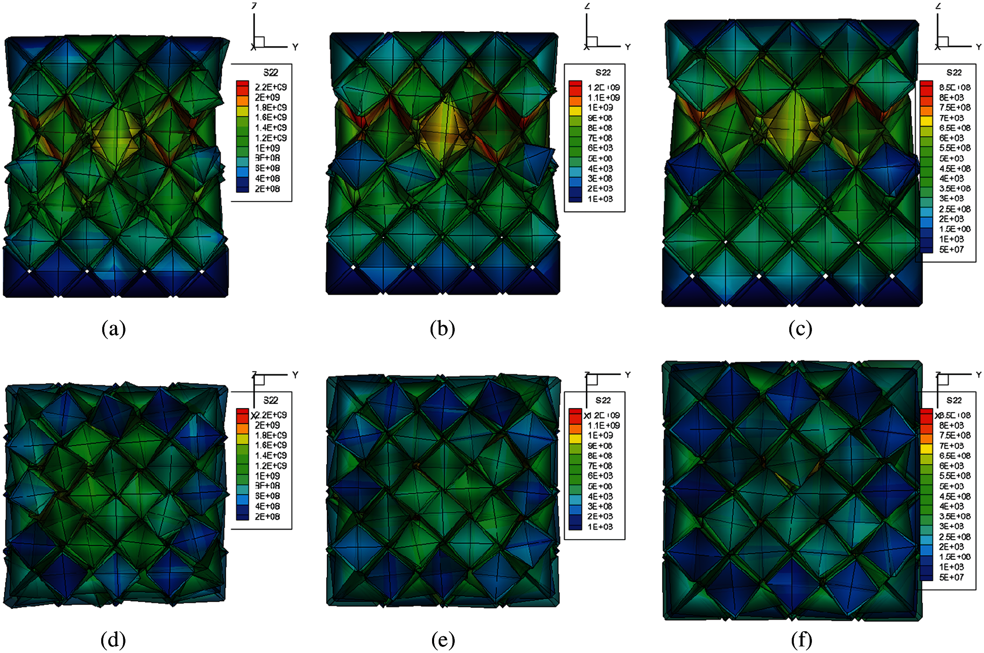
Figure 11: The von-Mise stress distributions in (100) and (001) planes at the maximum loading points: (a), (d) for 20% strain unloading; (b), (e); for 15% strain unloading, and (c), (f) for 10% strain unloading
Similar to the pure tension case, we also conducted pure shear test on an α-Ta specimen of
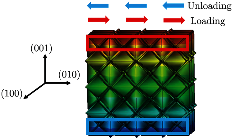
Figure 12: MCDD model under pure shear loading
By prescribing three different unloading strains, we can observe overall stress-strain relation in shear in comparable with that of MD simulations with the same loading and unloading conditions as shown in Fig. 13.
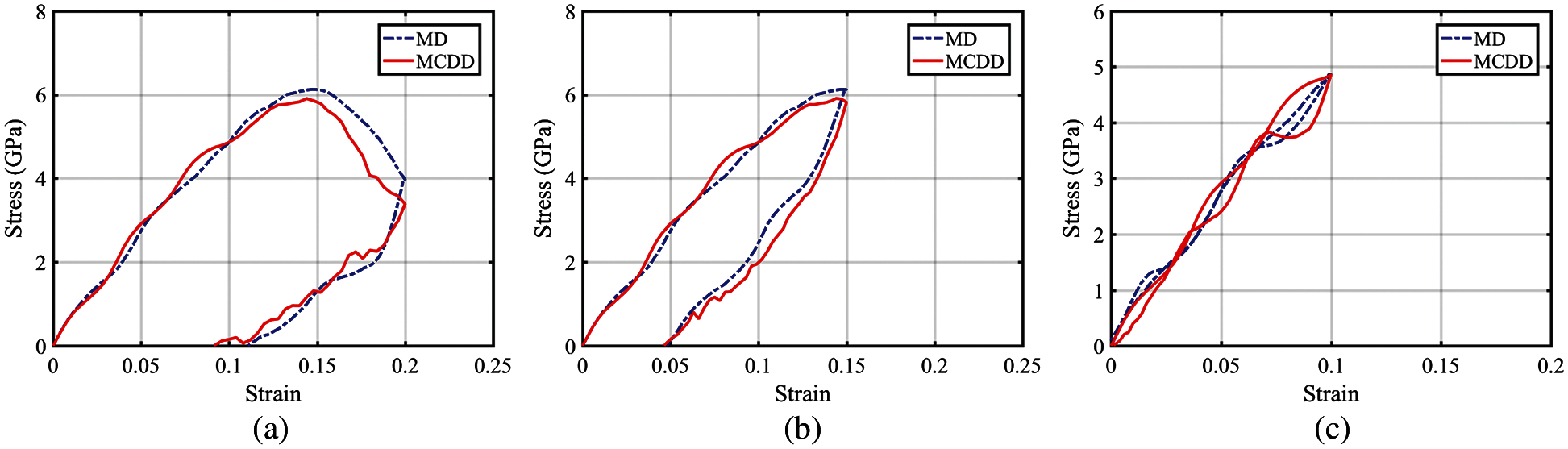
Figure 13: Shear stress-strain relations for three different unloading strain conditions: (a) at 20%. (b) at 15%. (c) at 10% shear strain unloading
Based on the results presented above, we may conclude that under pure shear loading MCDD method also offers consistent results with that obtained from MD simulations. It may be noted that in Fig. 14 the stress corresponding to the higher shear strain (maximum strain point) leads to higher residual stress.
5.2 The Relationship between Size Effect and Cross-Slip
Conventionally, size effect is not considered in constitutive relation therefore the corresponding stress-strain curve is smooth and continuous. However, with sample size decreasing to micron or sub-micron scale, material strength shows increased compared to macro-scale sample size. Some scholars give some statistical relations to describe size effect on material strength reduce. But until now, people are not clear what mechanism leads to size-effect of micron-scale materials.
Cross-slip is atomistic level phenomenon observed commonly in crystal plasticity especially when dislocation density attains to a certain value. Capturing cross-slip in micro-scale is not trivial, not to mention that cross-slip is observed in sub-micron scale.
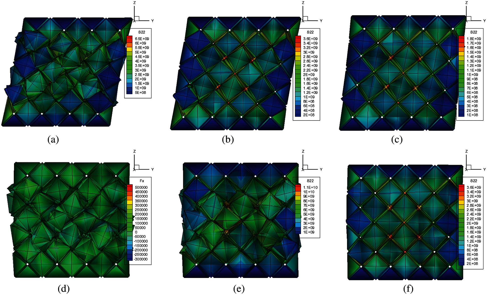
Figure 14: The von-Mise stress distribution respectively at the maximum strain point (a), (b), (c) and the residual strain point (d), (e), (f): (a), (d) for 20% strain unloading; (b), (e); for 15% strain unloading, and (c), (f) for 10% strain unloading
MCDD, as a multiscale method, has advantages in simulating crystal in micron-scale. Therefore, in this numerical example, we can find that cross-slip can be captured in numerical sample with different size. Furthermore, we give a preliminary conclusion that the appearance of cross-slip may lead to size effect in crystal plasticity.
Based on [16], we firstly constructed the same size MCDD model as comparison to validate our MCDD method. The MCDD model is shown as Fig. 15. The initial aspect ratio is 1:2:4, with dimension
From the figure above, we can find that the yielding stress of MCDD model is much lower than perfect crystal microstructure of MD simulation results and it is approximate to results of MD model with voids inserted. Based on the model above, we construct different size models to study relation between size effect and cross-slip.
From the Fig. 16, we can find that size effect in yielding stress: larger size model has lower yielding stress. Furthermore, we are able to capture cross-slip in sub-micron scale crystal. Based on Fig. 16, we can conclude that the appearance sequence of cross slip may lead to the appearance sequence of yielding stress, i.e., size effect.
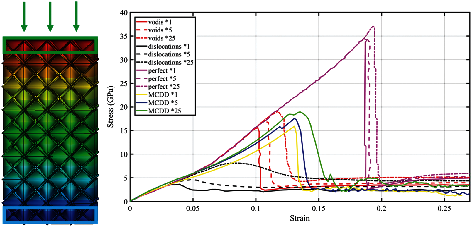
Figure 15: MCDD model and stress-strain curve comparison with MD simulation
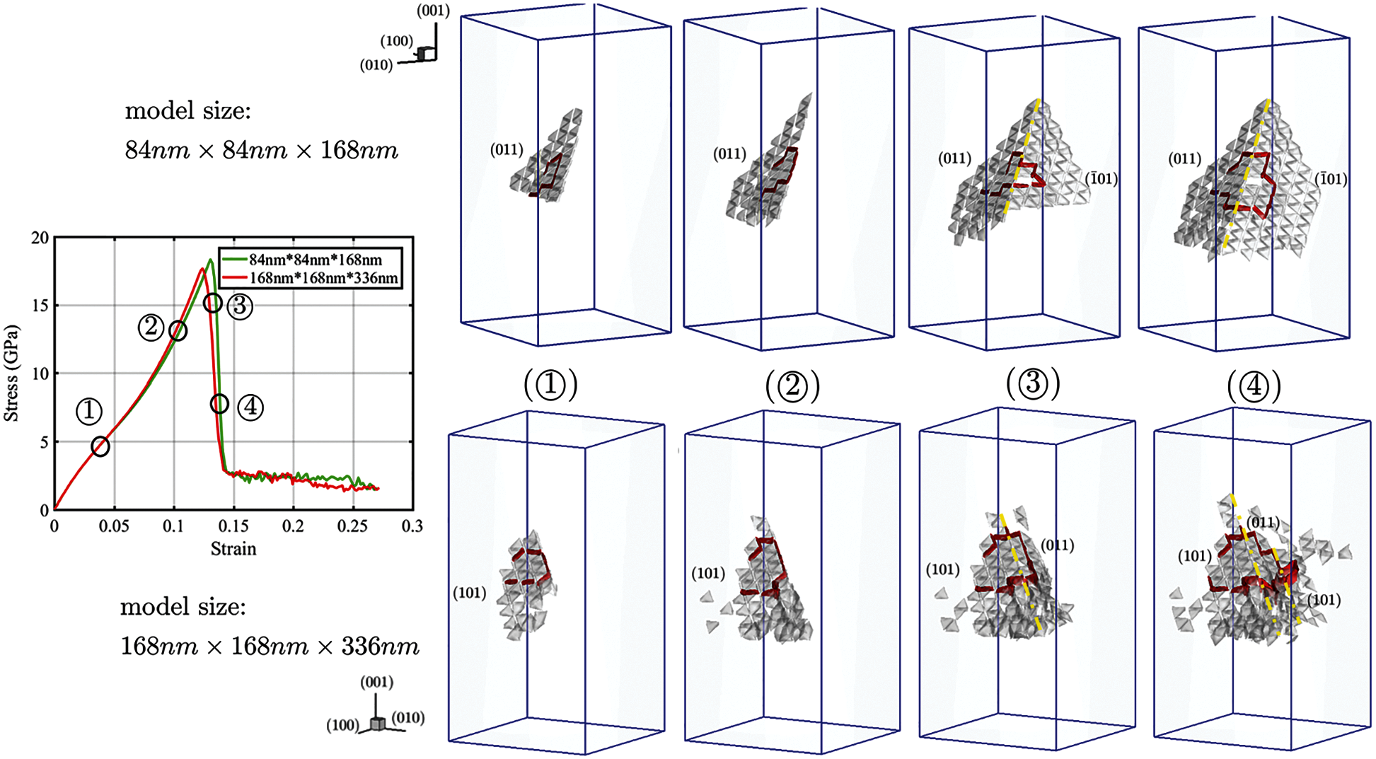
Figure 16: Stress-strain curve comparison and cross-slip observation
Based on such simulation result, we try to have the connection between size effect and cross-slip whose mechanism is following: initially when number of dislocation is few, crystal only has the primary slip plane. With strain increases, the number of dislocation in unit area (i.e., dislocation density) will increase. When dislocation density attains at a specific value, the second slip plane will be activated therefore the prerequisite of dislocation jumping (i.e., cross-slip) forms. Under this condition, dislocation will “jump” from one plane to another. Therefore, the cross-slip will be formed. Until now, MD simulation is hard to capture cross-slip but MCDD method can capure it. The reason may be that single or very few dislocations cannot activate second slip plane which is the prerequisite of cross-slip. But the MCDD method, as a multiscale method, simulates dislocation pattern which represents the ensemble or sub-network of dislocations. Therefore, MCDD method can capture that formation of secondary slip plane and “jumping” of dislocation.
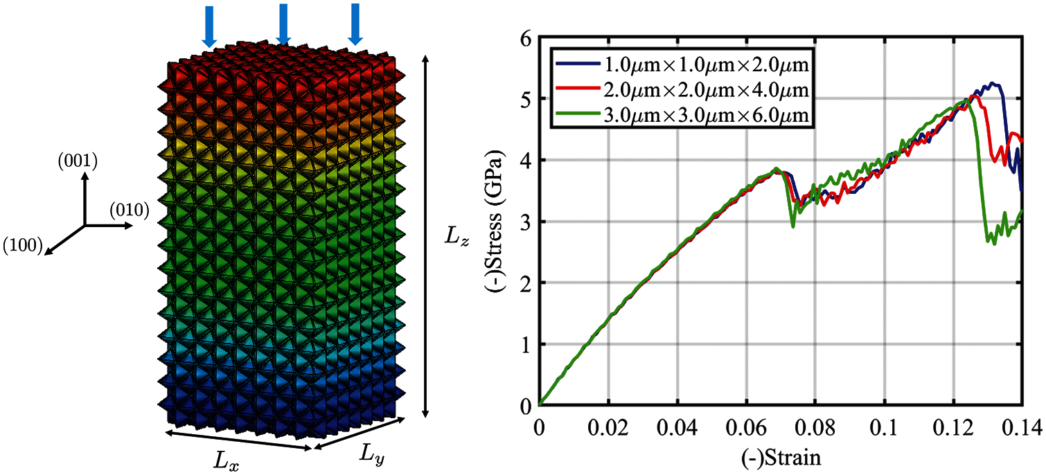
Figure 17: (a) MCDD FEM model and (b) Comparison of the stress-strain relations obtained from specimens of four different sizes
Based on analysis above, we know that dislocation density will activate cross-slip, the appearance sequence of cross-slip may determines the appearance sequence of yielding stress of materials and the difference among appearance sequence of yielding stress is the size effect. By this conclusion, we establish the connection between dislocation density and size effect and offer a preliminary explanation to size effect in micron-scale crystal sample.
5.3 Size Effect in Micron Scale Crystal Plasticity
At nanometer or sub-micron scale, a very strong size effect of crystal plasticity has been reported in experiments, e.g., [17]. In the following, we report a preliminary study on size-effect of meso-scale plasticity observed in MCDD simulations of a compression test of α-Ta.
We constructed three different MCDD numerical specimens at micron scale, and they are square columns with fixed length-to-cross section width ratio of 2:1. The four specimens have the sizes: Lx× Ly × Lz = 1.0 μm × 1.0 μm × 2.0 μm, 2.0 μm × 2.0 μm × 4.0 μm, and 3.0 μm × 3.0 μm × 6.0 μm as shown in Fig. 17a.
In this micron-scale MCDD specimen, it has 5952 tetrahedron elements (bulk crystal elements), 4096 wedge elements (1st order process zone or wedge dislocation pattern elements), 2752 prism elements (2nd order process zone or prim dislocation pattern elements), and 367 truncated octahedron elements (3rd process zone or truncated octahedron dislocation pattern elements). We then conducted uniaxial compression tests with prescribed displacement boundary condition with the loading strain rate: 5× 10 − 6 ps−1.
The stress-strain curves of α-Ta micropillar are shown in Fig. 17b. The yielding stress exhibits an increase with decreasing the size of MCDD specimen. The similar tendency have been observed in Abad et al. [17] in experiments. The increase in yield strength of micropillar might have been attributed to the variance of surface energy with micropillar size [18] as well as the less chance for defects.
In this work, we have further developed the recently proposed multiscale dislocation pattern dynamics by carrying out meso-scale discrete dislocation pattern dynamics computations and simulating crystal plasticity in α-Ta at the length scale up to 3.0 μm × 3.0 μm × 6.0 μm, which is beyond the capacity of conventional molecular dynamics simulations. Moreover, we have demonstrated that as a dislocation pattern dynamics, MCDD method can capture the size effect of crystal plasticity, and accurately capture cross-slip in BCC crystals. Based on the numerical simulation results discussed above, we have found that MCDD simulation has almost the same accuracy with that of molecular dynamics, but higher computation efficiency. This allows us to study mesoscale crystal plasticity at micron scale, i.e., 3.0 μm3 above, which is not reachable for MD simulations under current computer technology.
This work is highlighted by following two advances: (1) The simulated model is able to show accurate inelastic stress-strain curve comparable to MD results, and we can even capture dislocation nucleation and growth process with obvious crystal plasticity. There is a significant development in computational efficiency, which allows us to imagine further step: simulation of super micron-scale model and comparing with experiment results; (2) MCDD method shows the potential to be used to simulate the macroscale inelastic deformation process and fatigue damage, (3) MCDD successfully capture cross-slip which is hard to be observed in MD simulations. And having a preliminary relation between cross-slip and size effect lead us to have a preliminary explanation to mechanism of size effect and (4) MCDD model demonstrates that it can successfully capture size effect of up to 3.0 μm3 micropillar crystal model, which shows validity of MCDD method in simulating crystal plasticity.
However, the method still has some unresolved issues. For example, the thermal effect that is strongly influenced dislocation nucleation and growth has not been taken into account in the present dislocation pattern dynamics. Moreover for macro-scale dislocation pattern dynamics simulations, it will need massive MPI parallel computation to realize. For the above issues and more, we hope to deal with them in the subsequent work.
Funding Statement: The authors received no specific funding for this research.
Conflicts of Interest: The authors declare that they have no conflicts of interest to report regarding the present study.
1. Li, S., Ren, B., Minaki, H. (2014). Multiscale crystal defect dynamics: A dual-lattice process zone model. Philosophical Magazine, 94(13), 1414–1450. DOI 10.1080/14786435.2014.887859. [Google Scholar] [CrossRef]
2. Lyu, D., Li, S. (2017). Multiscale crystal defect dynamics: A coarse-grained lattice defect model based on crystal microstructure. Journal of the Mechanics and Physics of Solids, 107, 379–410. DOI 10.1016/j.jmps.2017.07.006. [Google Scholar] [CrossRef]
3. Lyu, D., Li, S. (2019). A multiscale dislocation pattern dynamics: Towards an atomistic-informed crystal plasticity theory. Journal of the Mechanics and Physics of Solids, 122, 613–632. DOI 10.1016/j.jmps.2018.09.025. [Google Scholar] [CrossRef]
4. Zhang, L. W., Xie, Y., Lyu, D., Li, S. (2019). Multiscale modeling of dislocation patterns and simulation of nanoscale plasticity in body-centered cubic (BCC) single crystals. Journal of the Mechanics and Physics of Solids, 130, 297–319. DOI 10.1016/j.jmps.2019.06.006. [Google Scholar] [CrossRef]
5. Kuhlmann-Wilsdorf, D., Hansen, N. (1991). Geometrically necessary, incidental and subgrain boundaries. Scripta Metallurgica et Materialia, 25(7), 1557–1562. DOI 10.1016/0956-716X(91)90451-6. [Google Scholar] [CrossRef]
6. Arsenlis, A., Parks, D. (1999). Crystallographic aspects of geometrically-necessary and statistically-stored dislocation density. Acta Materialia, 47(5), 1597–1611. DOI 10.1016/S1359-6454(99)00020-8. [Google Scholar] [CrossRef]
7. Buckman, R. (2000). New applications for tantalum and tantalum alloys. JOM, 52(3), 40–41. DOI 10.1007/s11837-000-0100-6. [Google Scholar] [CrossRef]
8. Black, J. (1994). Biologic performance of tantalum. Clinical Materials, 16(3), 167–173. DOI 10.1016/0267-6605(94)90113-9. [Google Scholar] [CrossRef]
9. Rowe, C. (1997). The use of tantalum in the process industry. Journal of Minerals, Metals and Materials Society, 49(1), 26–28. DOI 10.1007/BF02914624. [Google Scholar] [CrossRef]
10. Motz, C., Weygand, D., Senger, J., Gumbsch, P. (2009). Initial dislocation structures in 3-D discrete dislocation dynamics and their influence on microscale plasticity. Acta Materialia, 57(6), 1744–1754. DOI 10.1016/j.actamat.2008.12.020. [Google Scholar]
11. Ariza, M., Ortiz, M. (2005). Discrete crystal elasticity and discrete dislocations in crystals. Archive for Rational Mechanics and Analysis, 178(2), 149–226. DOI 10.1007/s00205-005-0391-4. [Google Scholar] [CrossRef]
12. Munkres, J. R. (2018). Elements of algebraic topology. Boca Raton, Florida: CRC press. [Google Scholar]
13. Hirani, A. N. (2003). Discrete exterior calculus (Ph.D. thesis). California Institute of Technology. [Google Scholar]
14. Chamati, H., Papanicolaou, N., Mishin, Y., Papaconstantopoulos, D. (2006). Embedded-atom potential for fe and its application to self-diffusion on Fe(1 0 0). Surface Science, 600(9), 1793–1803. DOI 10.1016/j.susc.2006.02.010. [Google Scholar] [CrossRef]
15. Zhou, X., Johnson, R., Wadley, H. (2004). Misfit-energy-increasing dislocations in vapor-deposited cofe/nife multilayers. Physical Review B, 69(14), 144113. DOI 10.1103/PhysRevB.69.144113. [Google Scholar] [CrossRef]
16. Zepeda-Ruiz, L. A., Stukowski, A., Oppelstrup, T., Bulatov, V. V. (2017). Probing the limits of metal plasticity with molecular dynamics simulations. Nature, 550(7677), 492–495. DOI 10.1038/nature23472. [Google Scholar] [CrossRef]
17. Abad, O. T., Wheeler, J. M., Michler, J., Schneider, A. S., Arzt, E. (2016). Temperature-dependent size effects on the strength of ta and w micropillars. Acta Materialia, 103, 483–494. DOI 10.1016/j.actamat.2015.10.016. [Google Scholar] [CrossRef]
18. Ren, J., Sun, Q., Xiao, L., Ding, X., Sun, J. (2014). Size-dependent of compression yield strength and deformation mechanism in titanium single-crystal nanopillars orientated [0001] and [1120]. Materials Science and Engineering: A, 615, 22–28. DOI 10.1016/j.msea.2014.07.065. [Google Scholar]
19. Featherston, F. H., Neighbours, J. (1963). Elastic constants of tantalum, tungsten, and molybdenum. Physical Review, 130(4), 1324. DOI 10.1103/PhysRev.130.1324. [Google Scholar] [CrossRef]
Appendix A. Elastic constant of Tantalum
In Appendix Table A1, we listed elastic constants of α-Ta obtained from both experiments [19] as well as the predictions from the EAM calculation.
 | This work is licensed under a Creative Commons Attribution 4.0 International License, which permits unrestricted use, distribution, and reproduction in any medium, provided the original work is properly cited. |